NCEP072N10 MOSFET Equivalente. Reemplazo. Hoja de especificaciones. Principales características
Número de Parte: NCEP072N10
Tipo de FET: MOSFET
Polaridad de transistor: N
ESPECIFICACIONES MÁXIMAS
Pdⓘ - Máxima disipación de potencia: 125 W
|Vds|ⓘ - Voltaje máximo drenador-fuente: 100 V
|Vgs|ⓘ - Voltaje máximo fuente-puerta: 20 V
|Id|ⓘ - Corriente continua de drenaje: 90 A
Tjⓘ - Temperatura máxima de unión: 175 °C
CARACTERÍSTICAS ELÉCTRICAS
trⓘ - Tiempo de subida: 11 nS
Cossⓘ - Capacitancia de salida: 335 pF
RDSonⓘ - Resistencia estado encendido drenaje a fuente: 0.0072 Ohm
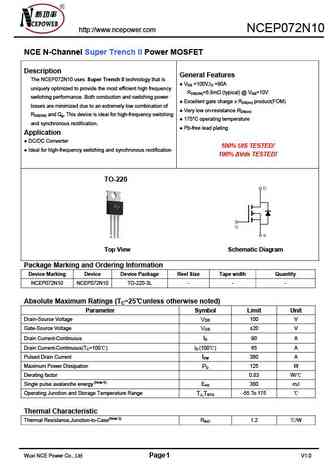
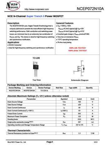
Encapsulados: TO220
Búsqueda de reemplazo de NCEP072N10 MOSFET
- Selecciónⓘ de transistores por parámetros
NCEP072N10 datasheet
ncep072n10.pdf
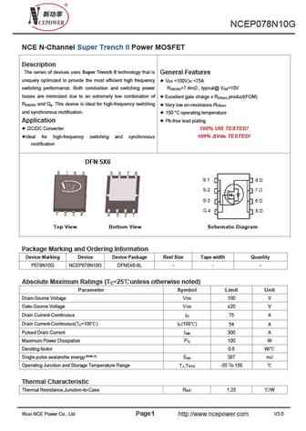
http //www.ncepower.com NCEP072N10 NCE N-Channel Super Trench II Power MOSFET Description General Features The NCEP072N10 uses Super Trench II technology that is VDS =100V,ID =90A uniquely optimized to provide the most efficient high frequency RDS(ON)=6.8m (typical) @ VGS=10V switching performance. Both conduction and switching power Excellent gate charge x RDS(on) p
ncep072n10a.pdf
http //www.ncepower.com NCEP072N10A NCE N-Channel Super Trench II Power MOSFET Description General Features The NCEP072N10A uses Super Trench II technology that is V =100V,I =88A DS D uniquely optimized to provide the most efficient high frequency R =6.2m (typical) @ V =10V DS(ON) GS switching performance. Both conduction and switching power R =8.4m (typical) @ V =4.5V DS(ON) GS
ncep075n85agu.pdf
NCEP075N85AGU NCE N-Channel Super Trench II Power MOSFET Description General Features The series of devices uses Super Trench II technology that is VDS =85V,ID =75A uniquely optimized to provide the most efficient high frequency RDS(ON)=5.6m , typical @ VGS=10V switching performance. Both conduction and switching power RDS(ON)=7.6m , typical @ VGS=4.5V losses are minimiz
ncep075n85gu.pdf
NCEP075N85GU NCE N-Channel Super Trench II Power MOSFET Description General Features The series of devices uses Super Trench II technology that is V =85V,I =75A DS D uniquely optimized to provide the most efficient high frequency R =5.6m , typical @ V =10V DS(ON) GS switching performance. Both conduction and switching power losses are minimized due to an extremely low combinati


Otros transistores... NCEP055N85 , NCEP055N85D , NCEP058N85 , NCEP058N85D , NCEP065N85 , NCEP068N10AG , NCEP068N10AK , NCEP068N10G , IRF530 , NCEP12T12 , NCEP12T12D , NCEP1520 , NCEP1545G , NCEP1545K , NCEP1570 , NCEP1570D , NCEP1580 .
🌐 : EN ES РУ

Liste
Recientemente añadidas las descripciónes de los transistores:
MOSFET: AUB062N08BG | AUB060N08AG | AUB056N10 | AUB056N08BGL | AUB050N085 | AUB050N055 | AUB045N12 | AUB045N10BT | AUB039N10 | AUB034N10 | AUB033N08BG | AUB026N085 | AUA062N08BG | AUA060N08AG | AUA056N08BGL | AUA039N10
Popular searches
nsd134 | 60r190p datasheet | cs30n20 datasheet | go42n10 | 2sa970 datasheet | 2sc1627 | aoe6936 datasheet | g40t60an3h datasheet