HM20N50A MOSFET Equivalente. Reemplazo. Hoja de especificaciones. Principales características
Número de Parte: HM20N50A
Tipo de FET: MOSFET
Polaridad de transistor: N
ESPECIFICACIONES MÁXIMAS
Pdⓘ - Máxima disipación de potencia: 280
W
|Vds|ⓘ - Voltaje máximo drenador - fuente: 500
V
|Vgs|ⓘ - Voltaje máximo fuente - puerta: 30
V
|Id|ⓘ - Corriente continua de drenaje: 20
A
Tjⓘ - Temperatura máxima de unión: 150
°C
CARACTERÍSTICAS ELÉCTRICAS
trⓘ - Tiempo de subida: 400
nS
Cossⓘ - Capacitancia
de salida: 400
pF
Rds(on)ⓘ - Resistencia estado encendido drenaje a fuente: 0.26
Ohm
Paquete / Cubierta:
TO3P
Búsqueda de reemplazo de HM20N50A MOSFET
-
Selección ⓘ de transistores por parámetros
HM20N50A datasheet
..1. Size:786K cn hmsemi
hm20n50a.pdf 
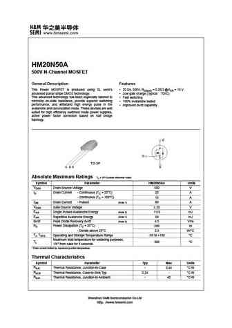
500V N-Channel MOSFET General Description Features This Power MOSFET is produced using SL semi s 20.0A, 500V, RDS(on) = 0.26 @VGS = 10 V advanced planar stripe DMOS technology. Low gate charge ( typical 70nC) This advanced technology has been especially tailored to Fast switching minimize on-state resistance, provide superior switching 100% avalanche tested
7.1. Size:863K cn hmsemi
hm20n50f.pdf
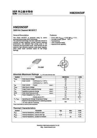
500V N-Channel MOSFET General Description Features This Power MOSFET is produced using SL semi s 20.0A, 500V, RDS(on) = 0.26 @VGS = 10 V advanced planar stripe DMOS technology. Low gate charge ( typical 70nC) This advanced technology has been especially tailored to Fast switching minimize on-state resistance, provide superior switching 100% avalan
9.1. Size:97K chenmko
chm20n06pagp.pdf
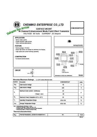
CHENMKO ENTERPRISE CO.,LTD CHM20N06PAGP SURFACE MOUNT N-Channel Enhancement Mode Field Effect Transistor VOLTAGE 60 Volts CURRENT 20 Ampere APPLICATION * Servo motor control. * Power MOSFET gate drivers. * Other switching applications. D-PAK(TO-252) FEATURE * Small package. (TO-252) * Super high dense cell design for extremely low RDS(ON). .094 (2.40) .280 (7.10) * High power
9.2. Size:733K jiaensemi
jfhm20n60e.pdf
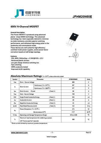
JFHM20N60E 600V N-Channel MOSFET General Description This Power MOSFET is produced using advanced planar stripe DMOS technology. This advanced technology has been especially tailored to minimize on-state resistance, provide superior switching performance, and withstand high energy pulse in the avalanche and commutation mode. These devices are well suited for high efficiency
9.3. Size:711K jiaensemi
jfhm20n60c.pdf
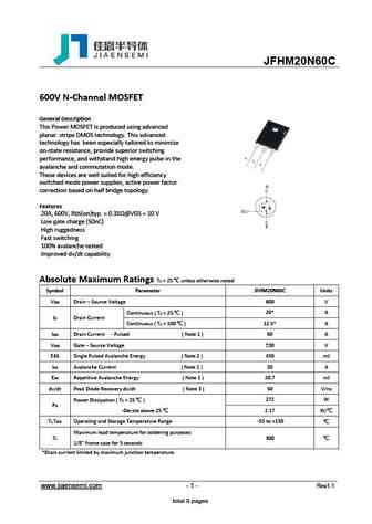
JFHM20N60C 600V N-Channel MOSFET General Description This Power MOSFET is produced using advanced planar stripe DMOS technology. This advanced technology has been especially tailored to minimize on-state resistance, provide superior switching performance, and withstand high energy pulse in the avalanche and commutation mode. These devices are well suited for high efficiency
9.4. Size:830K cn hmsemi
hm20n15a.pdf

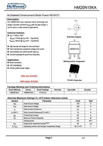
HM20N15A N-Channel Enhancement Mode Power MOSFET Description The HM20N15A uses advanced trench technology and design to provide excellent RDS(ON) with low gate charge. It can be used in a wide variety of applications. General Features VDS = 150V,ID =20A Schematic diagram RDS(ON)
9.5. Size:526K cn hmsemi
hm20n60a.pdf

HM20N60A VDSS 600 V General Description ID 20 A HM20N60A, the silicon N-channel Enhanced PD(TC=25 ) 250 W VDMOSFETs, is obtained by the self-aligned planar Technology RDS(ON)Typ 0.36 which reduce the conduction loss, improve switching performance and enhance the avalanche energy. The transistor can be used in various power switching circuit for system miniaturiza
9.6. Size:394K cn hmsemi
hm20n15.pdf

HM20N15 NCE N-Channel Enhancement Mode Power MOSFET Description The uses advanced trench technology and design to provide excellent RDS(ON) with low gate charge. It can be used in a wide variety of applications. General Features VDS = 150V,ID =20A RDS(ON)
9.7. Size:808K cn hmsemi
hm20n120tb.pdf
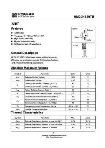
IGBT Features 1200V,20A VCE(sat)(typ.)=2.7V@VGE=15V,IC=20A High speed switching Higher system efficiency Soft current turn-off waveforms General Description KEDA PT IGBTs offer lower losses and higher energy efficiency for application such as IH (induction heating), and other soft switching applications. Absolute Maximum Ratings Sym
9.8. Size:962K cn hmsemi
hm20n120t.pdf
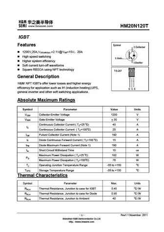
HM20N120T Typical Performance Characteristics Figure1 maximum DC collector current Figure2 power dissipation VS. case temprature VS. case temprature Figure3 forward SOA,TC=25 ,TJ 150 Figure4 reverse bias SOA,TJ=150 ,VGE=15V - 3 - Rev1.1 November. 2011 Shenzhen H&M Semiconductor Co.Ltd http //www.hmsemi.com HM20N120T Figure5 typical IGBT output characteristics, Fi
9.9. Size:655K cn hmsemi
hm20n06.pdf
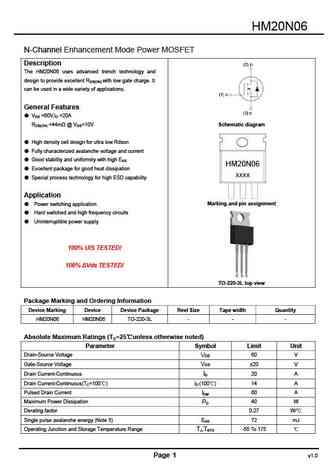
N-Channel Enhancement Mode Power MOSFET Description The uses advanced trench technology and design to provide excellent RDS(ON) with low gate charge. It can be used in a wide variety of applications. General Features VDS =60V,ID =20A RDS(ON)
9.10. Size:810K cn hmsemi
hm20n60.pdf

20N60 VDSS 600 V General Description ID 20 A HM20N60, the silicon N-channel Enhanced PD(TC=25 ) 250 W VDMOSFETs, is obtained by the self-aligned planar Technology RDS(ON)Typ 0.36 which reduce the conduction loss, improve switching performance and enhance the avalanche energy. The transistor can be used in various power switching circuit for system miniaturizati
9.11. Size:798K cn hmsemi
hm20n120ab.pdf
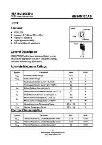
IGBT Features 1200V,20A VCE(sat)(typ.)=2.7V@VGE=15V,IC=20A High speed switching Higher system efficiency Soft current turn-off waveforms General Description KEDA PT IGBTs offer lower losses and higher energy efficiency for application such as IH (induction heating), and other soft switching applications. Absolute Maximum Ratings Symbol
9.12. Size:869K cn hmsemi
hm20n65f.pdf
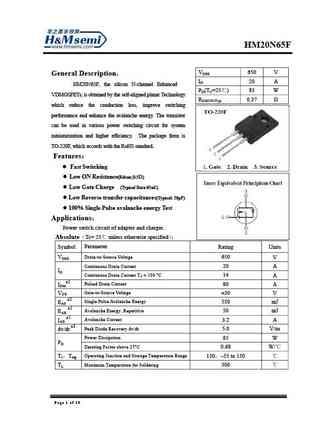
V General Description VDSS 650 ID 20 A HM20N65F, the silicon N-channel Enhanced PD(TC=25 ) 85 W VDMOSFETs, is obtained by the self-aligned planar Technology RDS(ON)Typ 0.37 which reduce the conduction loss, improve switching performance and enhance the avalanche energy. The transistor can be used in various power switching circuit for system miniaturizati
9.13. Size:620K cn hmsemi
hm20n15ka.pdf
HM20N15KA N-Channel Enhancement Mode Power MOSFET Description The HM20N15KA uses advanced trench technology and design to provide excellent RDS(ON) with low gate charge. It can be used in a wide variety of applications. General Features VDS = 150V,ID =20A Schematic diagram RDS(ON)
9.14. Size:877K cn hmsemi
hm20n15d.pdf

HM20N15D N-Channel Enhancement Mode Power MOSFET Description The HM20N15D uses advanced trench technology and design to provide excellent RDS(ON) with low gate charge. It can be used in a wide variety of applications. General Features VDS =150V,ID =20A RDS(ON)
9.15. Size:517K cn hmsemi
hm20n15k.pdf

HM20N15K Description The HM20N15K uses advanced trench technology and design to provide excellent RDS(ON) with low gate charge. It can be used in a wide variety of applications. General Features VDS = 150V,ID =20A RDS(ON)
9.16. Size:544K cn hmsemi
hm20n06ka.pdf
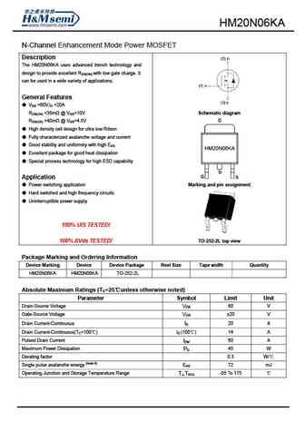
HM20N06KA N-Channel Enhancement Mode Power MOSFET Description The HM20N06KA uses advanced trench technology and design to provide excellent RDS(ON) with low gate charge. It can be used in a wide variety of applications. General Features VDS =60V,ID =20A RDS(ON)
9.17. Size:565K cn hmsemi
hm20n06ia.pdf

N-Channel Enhancement Mode Power MOSFET Description The uses advanced trench technology and design to provide excellent RDS(ON) with low gate charge. It can be used in a wide variety of applications. General Features VDS =60V,ID =20A Schematic diagram RDS(ON)
9.18. Size:920K cn hmsemi
hm20n60f.pdf
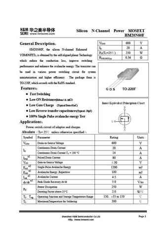
Silicon N-Channel Power MOSFET HM20N60F VDSS 600 V General Description ID 20 A HM20N60F, the silicon N-channel Enhanced PD(TC=25 ) 250 W VDMOSFETs, is obtained by the self-aligned planar Technology RDS(ON)Typ 0.36 which reduce the conduction loss, improve switching performance and enhance the avalanche energy. The transistor can be used in various power switching
Otros transistores... HM20N06
, HM20N06IA
, HM20N06KA
, HM20N15
, HM20N15A
, HM20N15D
, HM20N15K
, HM20N15KA
, 20N50
, HM20N50F
, HM20N60
, HM20N60A
, HM20N60F
, HM20N65F
, HM20P02D
, HM20P02Q
, HM20PD05
.


