HM2302A MOSFET Equivalente. Reemplazo. Hoja de especificaciones. Principales características
Número de Parte: HM2302A
Tipo de FET: MOSFET
Polaridad de transistor: N
ESPECIFICACIONES MÁXIMAS
Pdⓘ - Máxima disipación de potencia: 1 W
|Vds|ⓘ - Voltaje máximo drenador-fuente: 20 V
|Vgs|ⓘ - Voltaje máximo fuente-puerta: 10 V
|Id|ⓘ - Corriente continua de drenaje: 2.9 A
Tjⓘ - Temperatura máxima de unión: 150 °C
CARACTERÍSTICAS ELÉCTRICAS
trⓘ - Tiempo de subida: 50 nS
Cossⓘ - Capacitancia de salida: 120 pF
RDSonⓘ - Resistencia estado encendido drenaje a fuente: 0.045 Ohm
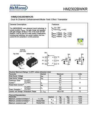
Encapsulados: SOT23
Búsqueda de reemplazo de HM2302A MOSFET
- Selecciónⓘ de transistores por parámetros
HM2302A datasheet
hm2302.pdf

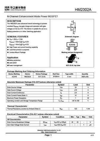
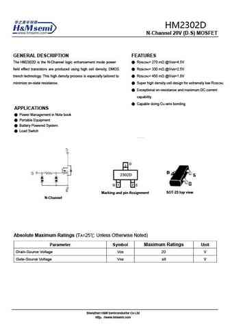
HM2302 N-Channel Enhancement Mode Power MOSFET DESCRIPTION D The HM2302 uses advanced trench technology to provide excellent RDS(ON), low gate charge and operation with gate G voltages as low as 2.5V. This device is suitable for use as a Battery protection or in other Switching application. S Schematic diagram GENERAL FEATURES VDS = 20V,ID = 2.9A D 3 RDS(ON)
hm2302bwsr.pdf
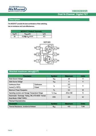
Description The MOSFET provide the best combination of fast switching, low on-resistance and cost-effectiveness. MOSFET Product Summary VDS(V) RDS(on)( ) ID(A) 20 0.29@ VGS=4.5V 0.5 SOT-563 S2 1 D2 6 G2 2 G1 5 4 S1 3 D1 Absolute maximum rating@25 Parameter Symbol Maximum Units Drain-Source Voltage
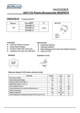
hm2302kr.pdf
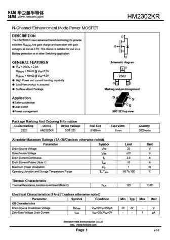
HM2302KR N-Channel Enhancement Mode Power MOSFET DESCRIPTION D The HM2302KR uses advanced trench technology to provide excellent RDS(ON), low gate charge and operation with gate G voltages as low as 2.5V. This device is suitable for use as a Battery protection or in other Switching application. S Schematic diagram GENERAL FEATURES VDS = 20V,ID = 2.9A D 3 RDS(ON)

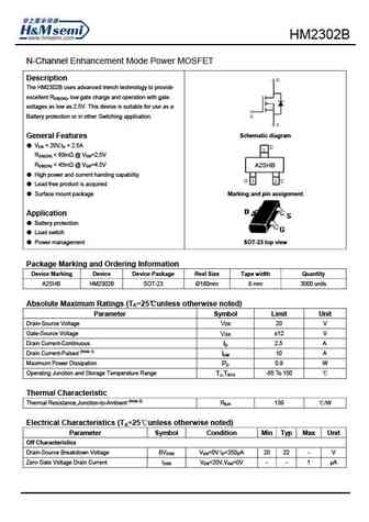
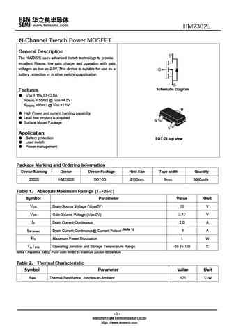
Otros transistores... HM2301BKR , HM2301BSR , HM2301C , HM2301D , HM2301DR , HM2301E , HM2301F , HM2302 , AO4407A , HM2302B , HM2302BJR , HM2302BWKR , HM2302BWSR , HM2302D , HM2302DR , HM2302E , HM2302F .
🌐 : EN ES РУ

Liste
Recientemente añadidas las descripciónes de los transistores:
MOSFET: AUN084N10 | AUN065N10 | AUN063N10 | AUN062N08BG | AUN060N08AG | AUN053N10 | AUN050N08BGL | AUN045N085 | AUN042N055 | AUN036N10 | AUD069N10A | AUD062N08BG | AUD060N08AG | AUD060N055 | AUD056N08BGL | AUB062N08BG
Popular searches
k3797 mosfet | bs170 datasheet | tip41c | irfp460 | irfz44n mosfet | lm317t datasheet | irf540 | bc337