HM2302BJR MOSFET Equivalente. Reemplazo. Hoja de especificaciones. Principales características
Número de Parte: HM2302BJR
Tipo de FET: MOSFET
Polaridad de transistor: N
ESPECIFICACIONES MÁXIMAS
Pdⓘ - Máxima disipación de potencia: 0.15 W
|Vds|ⓘ - Voltaje máximo drenador-fuente: 20 V
|Vgs|ⓘ - Voltaje máximo fuente-puerta: 12 V
|Id|ⓘ - Corriente continua de drenaje: 0.75 A
Tjⓘ - Temperatura máxima de unión: 150 °C
CARACTERÍSTICAS ELÉCTRICAS
trⓘ - Tiempo de subida: 4.8 nS
Cossⓘ - Capacitancia de salida: 13 pF
RDSonⓘ - Resistencia estado encendido drenaje a fuente: 0.38 Ohm
Encapsulados: SOT723
Búsqueda de reemplazo de HM2302BJR MOSFET
- Selecciónⓘ de transistores por parámetros
HM2302BJR datasheet
hm2302bjr.pdf
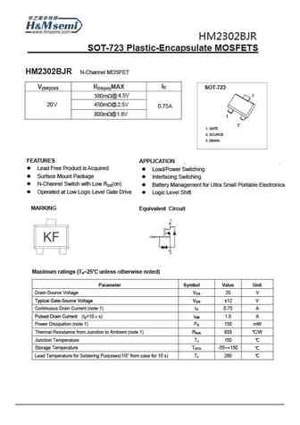
J HM2302BJR SOT-723 Plastic-Encapsulate MOSFETS HM2302BJR N-Channel MOSFET ID V(BR)DSS RDS(on)MAX SOT-723 380m @ 4.5V 20V 450m @2.5V 0.75A 800m @1.8V 1. GATE 2. SOURCE 3. DRAIN FEATURES APPLICATION Lead Free Product is Acquired Load/Power Switching Surface Mount Package Interfacing Switching N-Channel Switch with Low RDS(on) Battery Manage
hm2302bwsr.pdf
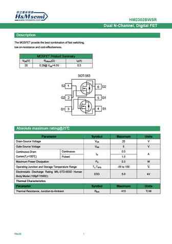
Description The MOSFET provide the best combination of fast switching, low on-resistance and cost-effectiveness. MOSFET Product Summary VDS(V) RDS(on)( ) ID(A) 20 0.29@ VGS=4.5V 0.5 SOT-563 S2 1 D2 6 G2 2 G1 5 4 S1 3 D1 Absolute maximum rating@25 Parameter Symbol Maximum Units Drain-Source Voltage
hm2302bwkr.pdf
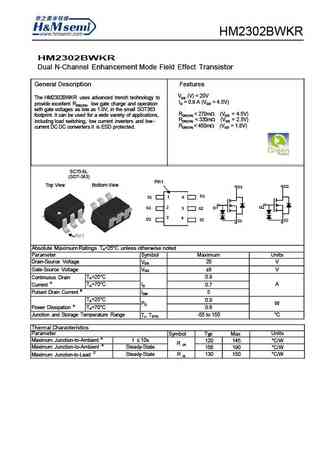
HM2302BWKR Dual N-Channel Enhancement Mode Field Effect Transistor General Description Features The HM2302BWKR uses advanced trench technology to VDS (V) = 20V ID = 0.9 A (VGS = 4.5V) excellent RDS(ON), low gate charge and operation voltages as low as 1.8V, in the small SOT363 RDS(ON)
hm2302b.pdf
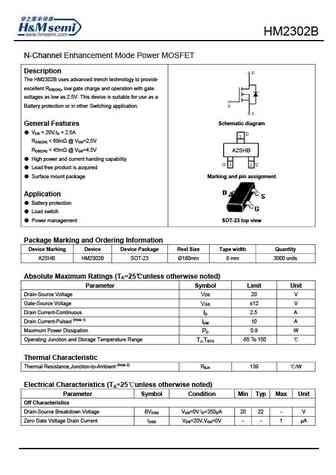
HM2302B N-Channel Enhancement Mode Power MOSFET Description The HM2302B uses advanced trench technology to provide excellent RDS(ON), low gate charge and operation with gate voltages as low as 2.5V. This device is suitable for use as a Battery protection or in other Switching application. Schematic diagram General Features VDS = 20V,ID = 2.5A RDS(ON)
Otros transistores... HM2301C , HM2301D , HM2301DR , HM2301E , HM2301F , HM2302 , HM2302A , HM2302B , IRFP064N , HM2302BWKR , HM2302BWSR , HM2302D , HM2302DR , HM2302E , HM2302F , HM2302KR , HM2305 .
🌐 : EN ES РУ

Liste
Recientemente añadidas las descripciónes de los transistores:
MOSFET: AUN084N10 | AUN065N10 | AUN063N10 | AUN062N08BG | AUN060N08AG | AUN053N10 | AUN050N08BGL | AUN045N085 | AUN042N055 | AUN036N10 | AUD069N10A | AUD062N08BG | AUD060N08AG | AUD060N055 | AUD056N08BGL | AUB062N08BG
Popular searches
tip41c | irfp460 | irfz44n mosfet | lm317t datasheet | irf540 | bc337 | ksc1845 | c1815 transistor