HM2310B MOSFET Equivalente. Reemplazo. Hoja de especificaciones. Principales características
Número de Parte: HM2310B
Tipo de FET: MOSFET
Polaridad de transistor: N
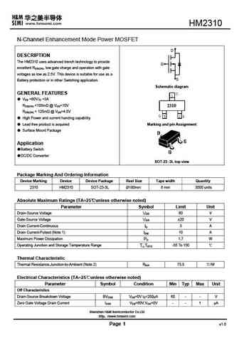
ESPECIFICACIONES MÁXIMAS
Pdⓘ - Máxima disipación de potencia: 1.8 W
|Vds|ⓘ - Voltaje máximo drenador-fuente: 60 V
|Vgs|ⓘ - Voltaje máximo fuente-puerta: 20 V
|Id|ⓘ - Corriente continua de drenaje: 4 A
Tjⓘ - Temperatura máxima de unión: 150 °C
CARACTERÍSTICAS ELÉCTRICAS
trⓘ - Tiempo de subida: 10 nS
Cossⓘ - Capacitancia de salida: 240 pF
RDSonⓘ - Resistencia estado encendido drenaje a fuente: 0.055 Ohm
Encapsulados: SOT23
Búsqueda de reemplazo de HM2310B MOSFET
- Selecciónⓘ de transistores por parámetros
HM2310B datasheet
hm2310b.pdf

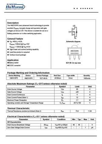
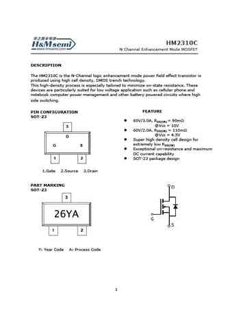
HM2310B N Channel Enhancement Mode MOSFET DESCRIPTION The HM2310B is the N-Channel logic enhancement mode power field effect transistor is produced using high cell density, DMOS trench technology. This high-density process is especially tailored to minimize on-state resistance. These devices are particularly suited for low voltage application such as cellular phone and notebook co
chm2310gp.pdf
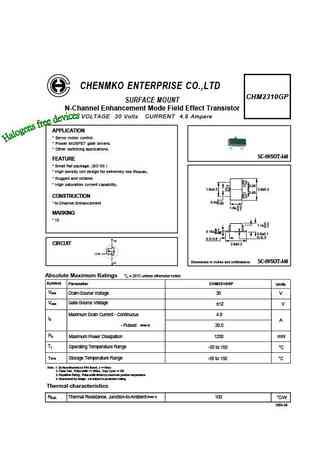
CHENMKO ENTERPRISE CO.,LTD CHM2310GP SURFACE MOUNT N-Channel Enhancement Mode Field Effect Transistor VOLTAGE 30 Volts CURRENT 4.8 Ampere APPLICATION * Servo motor control. * Power MOSFET gate drivers. * Other switching applications. SC-59/SOT-346 FEATURE * Small flat package. (SC-59 ) * High density cell design for extremely low RDS(ON). * Rugged and reliable. * High saturati
hm2310pr.pdf
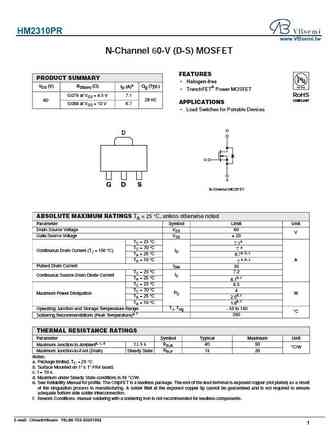
HM2310PR www.VBsemi.tw N-Channel 60-V (D-S) MOSFET FEATURES PRODUCT SUMMARY Halogen-free VDS (V) RDS(on) ( ) ID (A)a Qg (Typ.) TrenchFET Power MOSFET 0.076 at VGS = 4.5 V 7.1 RoHS 29 nC COMPLIANT 60 APPLICATIONS 0.088 at VGS = 10 V 6.7 Load Switches for Portable Devices D D G S G D S N-Channel MOSFET ABSOLUTE MAXIMUM RATINGS TA = 25 C, unless otherwise n
hm2310.pdf
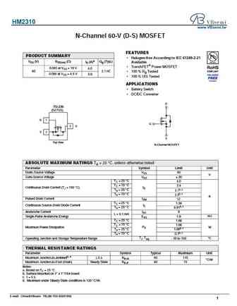
HM2310 www.VBsemi.tw N-Channel 60-V (D-S) MOSFET FEATURES PRODUCT SUMMARY Halogen-free According to IEC 61249-2-21 VDS (V) RDS(on) ( ) ID (A)a Qg (Typ.) Available TrenchFET Power MOSFET 0.085 at VGS = 10 V 4.0 60 2.1 nC 100 % Rg Tested 0.096 at VGS = 4.5 V 3.8 100 % UIS Tested APPLICATIONS Battery Switch DC/DC Converter D TO-236 (SOT23) G 1
Otros transistores... HM2306, HM2309, HM2309AL, HM2309APR, HM2309B, HM2309C, HM2309D, HM2309DR, AO3400, HM2310C, HM2312, HM2312B, HM2314, HM2314B, HM2318A, HM2318APR, HM2318B
🌐 : EN ES РУ

Liste
Recientemente añadidas las descripciónes de los transistores:
MOSFET: FTF30P35D | FTF25N35DHVT | FTF15N35D | FTE15C35G | FTP02P15G | FTE02P15G | AKF30N5P0SX | AKF30N10S | AKF20P45D | CM4407 | CM3407 | CM3400 | SVF11N65F | SVF11N65T | FKBB3105 | EHBA036R1
Popular searches
irfp250n | irf9540n | bd139 datasheet | irf9640 | 2n3053 | a1015 | mpsa42 | 2n5551 transistor