HM2312 MOSFET Equivalente. Reemplazo. Hoja de especificaciones. Principales características
Número de Parte: HM2312
Tipo de FET: MOSFET
Polaridad de transistor: N
ESPECIFICACIONES MÁXIMAS
Pdⓘ - Máxima
disipación de potencia: 1.25 W
|Vds|ⓘ - Voltaje máximo drenador-fuente: 20 V
|Vgs|ⓘ - Voltaje máximo fuente-puerta: 12 V
|Id|ⓘ - Corriente continua
de drenaje: 4.5 A
Tjⓘ - Temperatura máxima de unión: 150 °C
CARACTERÍSTICAS ELÉCTRICAS
trⓘ - Tiempo
de subida: 18 nS
Cossⓘ - Capacitancia de salida: 300 pF
RDSonⓘ - Resistencia estado encendido drenaje a fuente: 0.033 Ohm
Encapsulados: SOT23
Búsqueda de reemplazo de HM2312 MOSFET
- Selecciónⓘ de transistores por parámetros
HM2312 datasheet
..1. Size:554K cn hmsemi
hm2312.pdf 

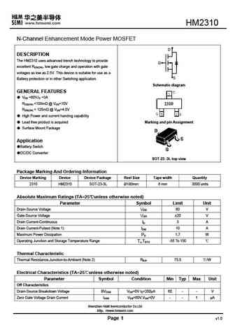
HM2312 N-Channel Enhancement Mode Power MOSFET Description D The HM2312 uses advanced trench technology to provide excellent RDS(ON), low gate charge and operation with gate G voltages as low as 2.5V. This device is suitable for use as a battery protection or in other switching application. S Schematic diagram General Features VDS = 20V,ID = 4.5A RDS(ON)
0.1. Size:648K cn hmsemi
hm2312b.pdf

HM2312B N-Channel Enhancement Mode Power MOSFET Description D The HM2312B uses advanced trench technology to provide excellent RDS(ON), low gate charge and operation with gate G voltages as low as 2.5V. This device is suitable for use as a battery protection or in other switching application. S Schematic diagram General Features VDS = 20V,ID = 4.5A RDS(ON)
9.1. Size:413K chenmko
chm2313qgp.pdf
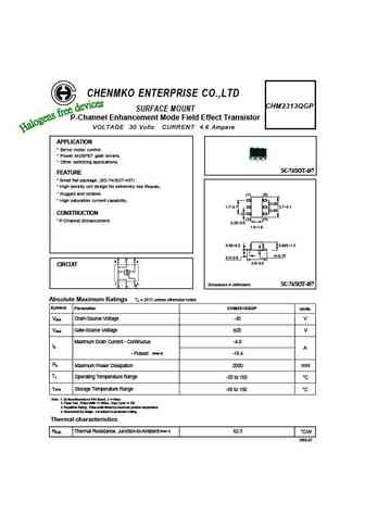
CHENMKO ENTERPRISE CO.,LTD CHM2313QGP SURFACE MOUNT P-Channel Enhancement Mode Field Effect Transistor VOLTAGE 30 Volts CURRENT 4.6 Ampere APPLICATION * Servo motor control. * Power MOSFET gate drivers. * Other switching applications. SC-74/SOT-457 FEATURE * Small flat package. (SC-74/SOT-457) * High density cell design for extremely low RDS(ON). * Rugged and reliable. (1) (6)
9.2. Size:69K chenmko
chm2316gp.pdf
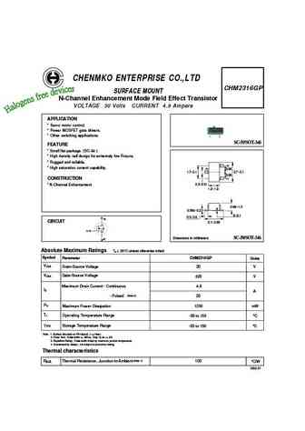
CHENMKO ENTERPRISE CO.,LTD CHM2316GP SURFACE MOUNT N-Channel Enhancement Mode Field Effect Transistor VOLTAGE 30 Volts CURRENT 4.8 Ampere APPLICATION * Servo motor control. * Power MOSFET gate drivers. * Other switching applications. SC-59/SOT-346 FEATURE * Small flat package. (SC-59 ) * High density cell design for extremely low RDS(ON). * Rugged and reliable. (2) * High sat
9.3. Size:108K chenmko
chm2316qgp.pdf
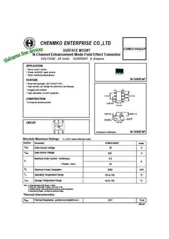
CHENMKO ENTERPRISE CO.,LTD CHM2316QGP SURFACE MOUNT N-Channel Enhancement Mode Field Effect Transistor VOLTAGE 30 Volts CURRENT 6 Ampere APPLICATION * Servo motor control. * Power MOSFET gate drivers. * Other switching applications. SC-74/SOT-457 FEATURE * Small flat package. (SC-74/SOT-457) * High density cell design for extremely low RDS(ON). * Rugged and reliable. (1) (6) *
9.4. Size:352K chenmko
chm2310gp.pdf
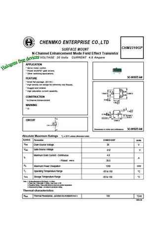
CHENMKO ENTERPRISE CO.,LTD CHM2310GP SURFACE MOUNT N-Channel Enhancement Mode Field Effect Transistor VOLTAGE 30 Volts CURRENT 4.8 Ampere APPLICATION * Servo motor control. * Power MOSFET gate drivers. * Other switching applications. SC-59/SOT-346 FEATURE * Small flat package. (SC-59 ) * High density cell design for extremely low RDS(ON). * Rugged and reliable. * High saturati
9.5. Size:74K chenmko
chm2314gp.pdf
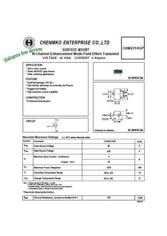
CHENMKO ENTERPRISE CO.,LTD CHM2314GP SURFACE MOUNT N-Channel Enhancement Mode Field Effect Transistor VOLTAGE 30 Volts CURRENT 4 Ampere APPLICATION * Servo motor control. * Power MOSFET gate drivers. * Other switching applications. SC-59/SOT-346 FEATURE * Small flat package. (SC-59 ) * High density cell design for extremely low RDS(ON). * Rugged and reliable. (2) * High satur
9.6. Size:90K chenmko
chm2313gp.pdf
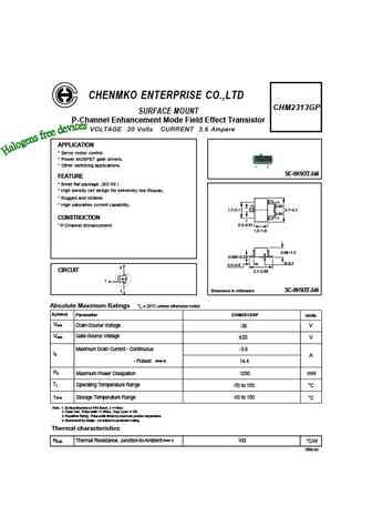
CHENMKO ENTERPRISE CO.,LTD CHM2313GP SURFACE MOUNT P-Channel Enhancement Mode Field Effect Transistor VOLTAGE 30 Volts CURRENT 3.6 Ampere APPLICATION * Servo motor control. * Power MOSFET gate drivers. * Other switching applications. SC-59/SOT-346 FEATURE * Small flat package. (SC-59 ) * High density cell design for extremely low RDS(ON). * Rugged and reliable. (2) * High sat
9.7. Size:154K chenmko
chm2313gp-a.pdf
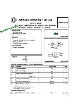
CHENMKO ENTERPRISE CO.,LTD CHM2313GP-A SURFACE MOUNT P-Channel Enhancement Mode Field Effect Transistor VOLTAGE 30 Volts CURRENT 3.6 Ampere APPLICATION * Servo motor control. * Power MOSFET gate drivers. * Other switching applications. SC-59/SOT-346 FEATURE * Small flat package. (SC-59 ) * High density cell design for extremely low RDS(ON). * Rugged and reliable. (2) * High s
9.8. Size:1675K cn vbsemi
hm2310pr.pdf
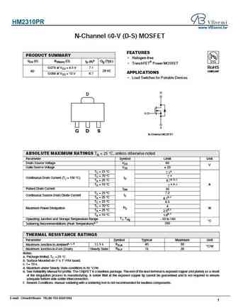
HM2310PR www.VBsemi.tw N-Channel 60-V (D-S) MOSFET FEATURES PRODUCT SUMMARY Halogen-free VDS (V) RDS(on) ( ) ID (A)a Qg (Typ.) TrenchFET Power MOSFET 0.076 at VGS = 4.5 V 7.1 RoHS 29 nC COMPLIANT 60 APPLICATIONS 0.088 at VGS = 10 V 6.7 Load Switches for Portable Devices D D G S G D S N-Channel MOSFET ABSOLUTE MAXIMUM RATINGS TA = 25 C, unless otherwise n
9.9. Size:1881K cn vbsemi
hm2310.pdf
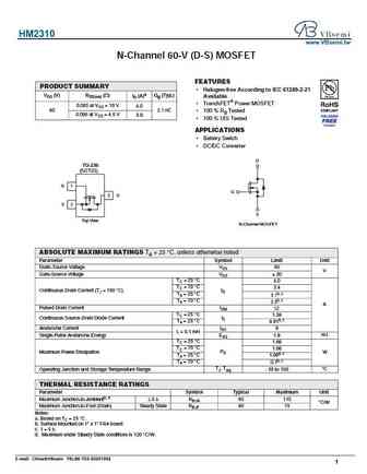
HM2310 www.VBsemi.tw N-Channel 60-V (D-S) MOSFET FEATURES PRODUCT SUMMARY Halogen-free According to IEC 61249-2-21 VDS (V) RDS(on) ( ) ID (A)a Qg (Typ.) Available TrenchFET Power MOSFET 0.085 at VGS = 10 V 4.0 60 2.1 nC 100 % Rg Tested 0.096 at VGS = 4.5 V 3.8 100 % UIS Tested APPLICATIONS Battery Switch DC/DC Converter D TO-236 (SOT23) G 1
9.10. Size:723K cn hmsemi
hm2310b.pdf

HM2310B N Channel Enhancement Mode MOSFET DESCRIPTION The HM2310B is the N-Channel logic enhancement mode power field effect transistor is produced using high cell density, DMOS trench technology. This high-density process is especially tailored to minimize on-state resistance. These devices are particularly suited for low voltage application such as cellular phone and notebook co
9.11. Size:402K cn hmsemi
hm2318b.pdf
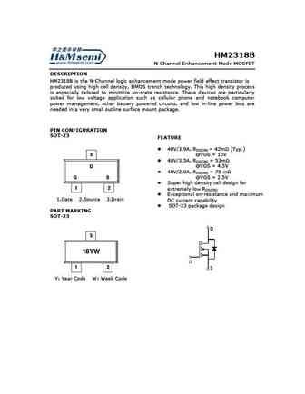
HM2318B N Channel Enhancement Mode MOSFET DESCRIPTION HM2318B is the N-Channel logic enhancement mode power field effect transistor is produced using high cell density, DMOS trench technology. This high density process is especially tailored to minimize on-state resistance. These devices are particularly suited for low voltage application such as cellular phone and notebook computer
9.12. Size:576K cn hmsemi
hm2310pr.pdf
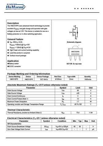
HM2310PR Description The HM2310PR uses advanced trench technology to provide D excellent RDS(ON), low gate charge and operation with gate voltages as low as 2.5V. This device is suitable for use as a G Battery protection or in other switching application. S General Feature VDS =60V,ID =4.0A Schematic diagram RDS(ON)
9.13. Size:514K cn hmsemi
hm2319a.pdf
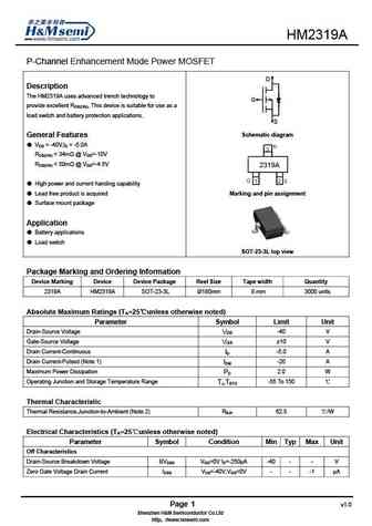
HM2319A P-Channel Enhancement Mode Power MOSFET D Description The HM2319A uses advanced trench technology to G provide excellent RDS(ON), This device is suitable for use as a load switch and battery protection applications. S Schematic diagram General Features VDS = -40V,ID = -5.0A RDS(ON)
9.14. Size:555K cn hmsemi
hm2314.pdf

HM2314 N-Channel Enhancement Mode Power MOSFET Description D The HM2314 uses advanced trench technology to provide excellent RDS(ON), low gate charge and operation with gate G voltages as low as 2.5V. This device is suitable for use as a battery protection or in other switching application. S Schematic diagram General Features VDS = 20V,ID = 4.5A RDS(ON)
9.15. Size:476K cn hmsemi
hm2310.pdf
HM2310 N-Channel Enhancement Mode Power MOSFET D DESCRIPTION The HM2310 uses advanced trench technology to provide G excellent RDS(ON), low gate charge and operation with gate voltages as low as 2.5V. This device is suitable for use as a S Battery protection or in other Switching application. Schematic diagram GENERAL FEATURES VDS =60V,ID =3A RDS(ON)
9.16. Size:711K cn hmsemi
hm2314b.pdf
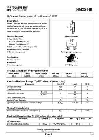
HM2314B N-Channel Enhancement Mode Power MOSFET Description D The HM2314B uses advanced trench technology to provide excellent RDS(ON), low gate charge and operation with gate G voltages as low as 2.5V. This device is suitable for use as a battery protection or in other switching application. S Schematic diagram General Features VDS = 20V,ID = 4.5A RDS(ON)
9.17. Size:1351K cn hmsemi
hm2318apr.pdf
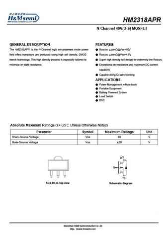
HM2318 N-Channel 40V(D-S) MOSFET GENERAL DESCRIPTION FEATURES The HM is the N-Channel logic enhancement mode power RDS(ON) 28m @VGS=10V field effect transistors are produced using high cell density, DMOS RDS(ON) 38m @VGS=4.5V trench technology. This high density process is especially tailored to Super high density cell design for extremely low RDS(ON)
9.18. Size:1187K cn hmsemi
hm2318a.pdf
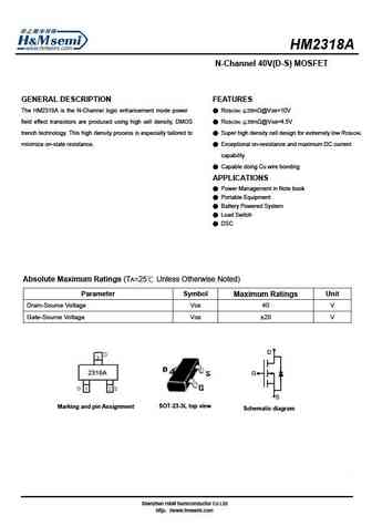
HM2318A N-Channel 40V(D-S) MOSFET GENERAL DESCRIPTION FEATURES The HM2318A is the N-Channel logic enhancement mode power RDS(ON) 28m @VGS=10V field effect transistors are produced using high cell density, DMOS RDS(ON) 38m @VGS=4.5V trench technology. This high density process is especially tailored to Super high density cell design for extremely low RDS(ON) min
9.19. Size:445K cn hmsemi
hm2319.pdf
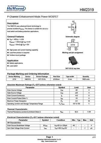
HM2319 P-Channel Enhancement Mode Power MOSFET D Description The HM2319 uses advanced trench technology to G provide excellent RDS(ON), This device is suitable for use as a load switch and battery protection applications. S Schematic diagram General Features VDS = -40V,ID = - A RDS(ON)
9.20. Size:719K cn hmsemi
hm2310c.pdf
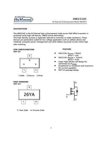
HM N Channel Enhancement Mode MOSFET DESCRIPTION The HM2310C is the N-Channel logic enhancement mode power field effect transistor is produced using high cell density, DMOS trench technology. This high-density process is especially tailored to minimize on-state resistance. These devices are particularly suited for low voltage application such as cellular phone and notebook co
Otros transistores... HM2309AL, HM2309APR, HM2309B, HM2309C, HM2309D, HM2309DR, HM2310B, HM2310C, IRF3710, HM2312B, HM2314, HM2314B, HM2318A, HM2318APR, HM2318B, HM2319, HM2319A
