HM3401C MOSFET Equivalente. Reemplazo. Hoja de especificaciones. Principales características
Número de Parte: HM3401C
Tipo de FET: MOSFET
Polaridad de transistor: P
ESPECIFICACIONES MÁXIMAS
Pdⓘ - Máxima disipación de potencia: 1 W
|Vds|ⓘ - Voltaje máximo drenador-fuente: 30 V
|Vgs|ⓘ - Voltaje máximo fuente-puerta: 20 V
|Id|ⓘ - Corriente continua de drenaje: 2.5 A
Tjⓘ - Temperatura máxima de unión: 150 °C
CARACTERÍSTICAS ELÉCTRICAS
trⓘ - Tiempo de subida: 9 nS
Cossⓘ - Capacitancia de salida: 47 pF
RDSonⓘ - Resistencia estado encendido drenaje a fuente: 0.13 Ohm
Encapsulados: SOT23
Búsqueda de reemplazo de HM3401C MOSFET
- Selecciónⓘ de transistores por parámetros
HM3401C datasheet
hm3401c.pdf
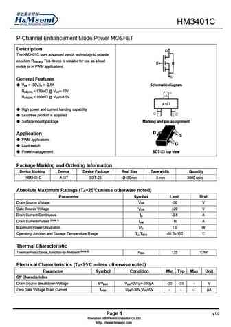
HM3401C P-Channel Enhancement Mode Power MOSFET Description D The HM3401C uses advanced trench technology to provide excellent RDS(ON), This device is suitable for use as a load G switch or in PWM applications. S General Features VDS = -30V,ID = -2.5A Schematic diagram RDS(ON)
hm3401.pdf
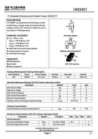
HM3401 P-Channel Enhancement Mode Power MOSFET DESCRIPTION D The HM3401 uses advanced trench technology to provide excellent RDS(ON), low gate charge and operation with gate G voltages as low as 2.5V. This device is suitable for use as a load switch or in PWM applications. S Schematic diagram GENERAL FEATURES VDS = -30V,ID = -4.2A RDS(ON)
hm3401d.pdf
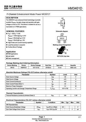
HM3401 P-Channel Enhancement Mode Power MOSFET DESCRIPTION D The HM3401 uses advanced trench technology to provide excellent RDS(ON), low gate charge and operation with gate G voltages as low as 2.5V. This device is suitable for use as a load switch or in PWM applications. S Schematic diagram GENERAL FEATURES VDS = -30V,ID = -4.6A RDS(ON)
hm3401b.pdf

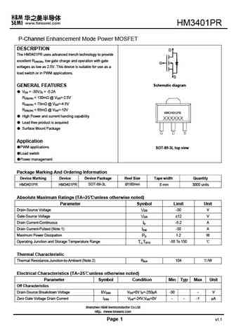
HM3401B P-Channel Enhancement Mode Power MOSFET DESCRIPTION D The HM3401B uses advanced trench technology to provide excellent RDS(ON), low gate charge and operation with gate G voltages as low as 2.5V. This device is suitable for use as a load switch or in PWM applications. S Schematic diagram GENERAL FEATURES VDS = -30V,ID = -4.2A RDS(ON)
Otros transistores... HM3307B, HM3400, HM3400B, HM3400C, HM3400D, HM3400DR, HM3401, HM3401B, IRFP260N, HM3401D, HM3401PR, HM3406B, HM3407A, HM3407B, HM3413, HM3413B, HM3414
🌐 : EN ES РУ

Liste
Recientemente añadidas las descripciónes de los transistores:
MOSFET: AKF30N5P0SX | AKF30N10S | AKF20P45D | CM4407 | CM3407 | CM3400 | SVF11N65F | SVF11N65T | FKBB3105 | EHBA036R1 | CRTT067N10N | AP6NA3R2MT | AP65SA145DDT8 | AP4NAR95CMT-A | AP4024GEMT-HF | AP3P050AH
Popular searches
9014 transistor | irfp260n datasheet | irfp250m | 2sk1058 | ss8550 | mje15033 | 2sc945 datasheet | a92 transistor