ME15N25 MOSFET Equivalente. Reemplazo. Hoja de especificaciones. Principales características
Número de Parte: ME15N25
Tipo de FET: MOSFET
Polaridad de transistor: N
ESPECIFICACIONES MÁXIMAS
Pdⓘ - Máxima disipación de potencia: 125 W
|Vds|ⓘ - Voltaje máximo drenador-fuente: 250 V
|Vgs|ⓘ - Voltaje máximo fuente-puerta: 25 V
|Id|ⓘ - Corriente continua de drenaje: 17.1 A
Tjⓘ - Temperatura máxima de unión: 150 °C
CARACTERÍSTICAS ELÉCTRICAS
trⓘ - Tiempo de subida: 62.6 nS
Cossⓘ - Capacitancia de salida: 112 pF
RDSonⓘ - Resistencia estado encendido drenaje a fuente: 0.265 Ohm
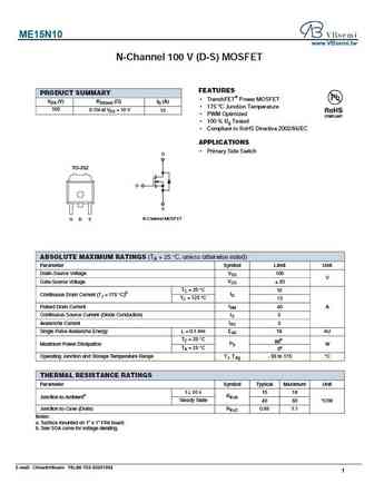
Encapsulados: TO252
Búsqueda de reemplazo de ME15N25 MOSFET
- Selecciónⓘ de transistores por parámetros
ME15N25 datasheet
me15n25 me15n25-g.pdf
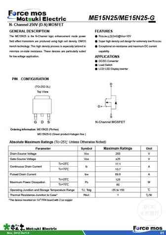
ME15N25/ME15N25-G N- Channel 250V (D-S) MOSFET GENERAL DESCRIPTION FEATURES The ME15N25 is the N-Channel logic enhancement mode power RDS(ON) 265m @VGS=10V field effect transistors are produced using high cell density, DMOS Super high density cell design for extremely low RDS(ON) trench technology. This high density process is especially tailored to Exceptional on-resi
me15n25f me15n25f-g.pdf
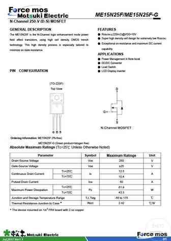
ME15N25F/ME15N25F-G N-Channel 250-V (D-S) MOSFET GENERAL DESCRIPTION FEATURES RDS(ON) 220m @VGS=10V The ME15N25F is the N-Channel logic enhancement mode power Super high density cell design for extremely low RDS(ON) field effect transistors, using high cell density, DMOS trench Exceptional on-resistance and maximum DC current technology. This high density process
me15n10 me15n10g.pdf
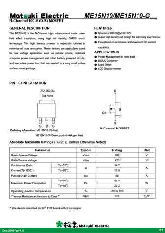
ME15N10/ME15N10-G N-Channel 100-V (D-S) MOSFET GENERAL DESCRIPTION FEATURES RDS(ON) 100m @VGS=10V The ME15N10 is the N-Channel logic enhancement mode power Super high density cell design for extremely low RDS(ON) field effect transistors, using high cell density, DMOS trench Exceptional on-resistance and maximum DC current technology. This high density process is
me15n10 me15n10-g.pdf
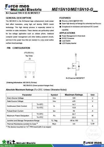
ME15N10/ME15N10-G N-Channel 100-V (D-S) MOSFET GENERAL DESCRIPTION FEATURES RDS(ON) 100m @VGS=10V The ME15N10 is the N-Channel logic enhancement mode power Super high density cell design for extremely low RDS(ON) field effect transistors, using high cell density, DMOS trench Exceptional on-resistance and maximum DC current technology. This high density process is
Otros transistores... ME100N03T-G, ME120N04T, ME1302AT3, ME1302AT3-G, ME1303AT3, ME1303AT3-G, ME13N10A, ME13N10A-G, IRF3710, ME15N25F, ME15N25F-G, ME15N25-G, ME200N04T, ME200N04T-G, ME20N10-G, ME20N15F, ME2301A
History: ME13N10A-G
🌐 : EN ES РУ

Liste
Recientemente añadidas las descripciónes de los transistores:
MOSFET: AKF30N5P0SX | AKF30N10S | AKF20P45D | CM4407 | CM3407 | CM3400 | SVF11N65F | SVF11N65T | FKBB3105 | EHBA036R1 | CRTT067N10N | AP6NA3R2MT | AP65SA145DDT8 | AP4NAR95CMT-A | AP4024GEMT-HF | AP3P050AH
Popular searches
toshiba c5198 | irf520n datasheet | tip107 | 2n5457 | k3568 | 2sc1344 | cs840f | 2n3053 equivalent