WM02DN70A MOSFET Equivalente. Reemplazo. Hoja de especificaciones. Principales características
Número de Parte: WM02DN70A
Tipo de FET: MOSFET
Polaridad de transistor: N
ESPECIFICACIONES MÁXIMAS
Pdⓘ - Máxima disipación de potencia: 1.5 W
|Vds|ⓘ - Voltaje máximo drenador-fuente: 20 V
|Vgs|ⓘ - Voltaje máximo fuente-puerta: 12 V
|Id|ⓘ - Corriente continua de drenaje: 7 A
Tjⓘ - Temperatura máxima de unión: 150 °C
CARACTERÍSTICAS ELÉCTRICAS
trⓘ - Tiempo de subida: 10.5 nS
Cossⓘ - Capacitancia de salida: 130 pF
RDSonⓘ - Resistencia estado encendido drenaje a fuente: 0.0135 Ohm
Encapsulados: TSSOP-8L
Búsqueda de reemplazo de WM02DN70A MOSFET
- Selecciónⓘ de transistores por parámetros
WM02DN70A datasheet
wm02dn70a.pdf
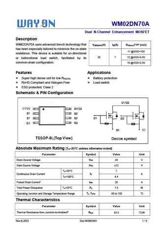
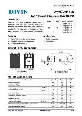
WM02DN70A Dual N-Channel Enhancement MOSFET Description WM02DN70A uses advanced trench technology that V (V) I (A) R TYP (m ) (BR)DSS D DS(on) has been especially tailored to minimize the on-state 11 @VGS=10V resistance. This device is suitable for un-directional 20 7 12 @VGS=4.5V or bidirectional load switch, facilitated by its common-drain configuration. 15 @VGS=2.5V
wm02dn70m3.pdf
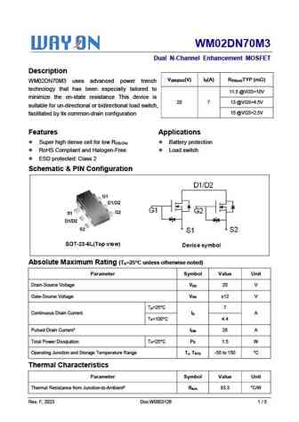
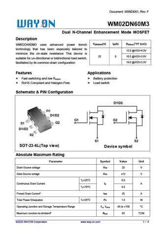
WM02DN70M3 Dual N-Channel Enhancement MOSFET Description V (V) I (A) R TYP (m ) (BR)DSS D DS(on) WM02DN70M3 uses advanced power trench technology that has been especially tailored to 11.5 @VGS=10V minimize the on-state resistance This device is 20 7 13 @VGS=4.5V suitable for un-directional or bidirectional load switch, 15 @VGS=2.5V facilitated by its common-drain config
wm02dn08t.pdf
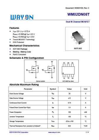
Document W0803109, Rev C WM02DN08T T Dual N-Channel MOSFET Features V = 20 V, I = 0.75 A DS D R
wm02dn560q.pdf
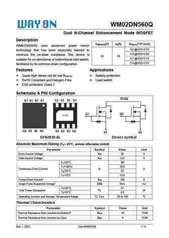
WM02DN560Q Dual N-Channel Enhancement Mode MOSFET Description V (V) I (A) R TYP (m ) (BR)DSS D DS(on) WM02DN560Q uses advanced power trench 4.2 @VGS=4.5V technology that has been especially tailored to 4.3 @VGS=3.9V minimize the on-state resistance This device is 20 56 4.7 @VGS=3.1V suitable for un-directional or bidirectional load switch, 5.0 @VGS=2.5V facilitated
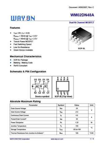
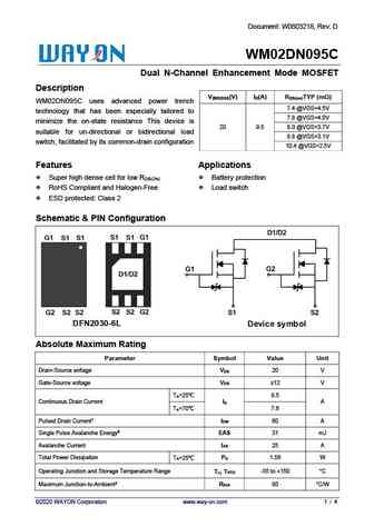
Otros transistores... WM02DN08D , WM02DN08T , WM02DN095C , WM02DN110C , WM02DN48A , WM02DN50M3 , WM02DN560Q , WM02DN60M3 , IRFB4227 , WM02DN70M3 , WM02DP06D , WM02N08F , WM02N08FB , WM02N08G , WM02N08H , WM02N08L , WM02N20F .
History: WMJ28N50C4 | WM02DN110C | VN0340N1
History: WMJ28N50C4 | WM02DN110C | VN0340N1
🌐 : EN ES РУ

Liste
Recientemente añadidas las descripciónes de los transistores:
MOSFET: ASU70R600E | ASU65R850E | ASU65R550E | ASU65R350E | ASR65R120EFD | ASR65R046EFD | ASQ65R046EFD | ASM65R280E | ASM60R330E | ASE70R950E | ASD80R750E | ASD70R950E | ASD70R600E | ASD70R380E | ASD65R850E | ASD65R550E
Popular searches
mn2488 | irfb438 | mj21193g | irf3710 pinout | irf9530 datasheet | mj21194 | oc71 transistor | 2n3440