FDS6676AS MOSFET Equivalente. Reemplazo. Hoja de especificaciones. Principales características
Número de Parte: FDS6676AS
Tipo de FET: MOSFET
Polaridad de transistor: N
ESPECIFICACIONES MÁXIMAS
Pdⓘ - Máxima
disipación de potencia: 2.5 W
|Vds|ⓘ - Voltaje máximo drenador-fuente: 30 V
|Vgs|ⓘ - Voltaje máximo fuente-puerta: 20 V
|Id|ⓘ - Corriente continua
de drenaje: 14.5 A
Tjⓘ - Temperatura máxima de unión: 150 °C
CARACTERÍSTICAS ELÉCTRICAS
trⓘ - Tiempo
de subida: 12 nS
Cossⓘ - Capacitancia de salida: 710 pF
RDSonⓘ - Resistencia estado encendido drenaje a fuente: 0.006 Ohm
Encapsulados: SO-8
Búsqueda de reemplazo de FDS6676AS MOSFET
- Selecciónⓘ de transistores por parámetros
FDS6676AS datasheet
..1. Size:841K fairchild semi
fds6676as.pdf 
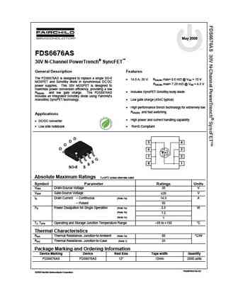
May 2008 tm FDS6676AS 30V N-Channel PowerTrench SyncFET General Description Features The FDS6676AS is designed to replace a single SO-8 14.5 A, 30 V. RDS(ON) max= 6.0 m @ VGS = 10 V MOSFET and Schottky diode in synchronous DC DC RDS(ON) max= 7.25 m @ VGS = 4.5 V power supplies. This 30V MOSFET is designed to maximize power conversion efficiency, providing a low
8.1. Size:295K fairchild semi
fds6670as.pdf
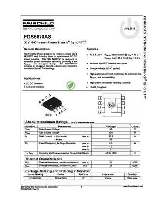
July 2010 FDS6670AS 30V N-Channel PowerTrench SyncFET General Description Features The FDS6670AS is designed to replace a single SO-8 13.5 A, 30 V. RDS(ON) max= 9.0 m @ VGS = 10 V MOSFET and Schottky diode in synchronous DC DC RDS(ON) max= 11.5 m @ VGS = 4.5 V power supplies. This 30V MOSFET is designed to maximize power conversion efficiency, providing a low Inclu
8.2. Size:93K fairchild semi
fds6679.pdf
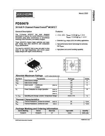
March 2005 FDS6679 30 Volt P-Channel PowerTrench MOSFET General Description Features This P-Channel MOSFET has been designed 13 A, 30 V. RDS(ON) = 9 m @ VGS = 10 V specifically to improve the overall efficiency of DC/DC RDS(ON) = 13 m @ VGS = 4.5 V converters using either synchronous or conventional switching PWM controllers, and battery chargers.
8.3. Size:505K fairchild semi
fds6675bz.pdf
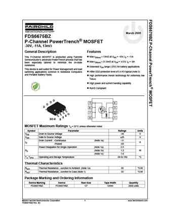
March 2009 FDS6675BZ tm P-Channel PowerTrench MOSFET -30V, -11A, 13m General Description Features Max rDS(on) = 13m at VGS = -10V, ID = -11A This P-Channel MOSFET is producted using Fairchild Semiconductor s advanced PowerTrench process that has Max rDS(on) = 21.8m at VGS = -4.5V, ID = -9A been especially tailored to minimize the on-state resistance. Extended VGS
8.4. Size:105K fairchild semi
fds6675a.pdf
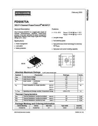
February 2003 FDS6675A 30V P-Channel PowerTrench MOSFET General Description Features This P-Channel MOSFET is a rugged gate version of 11 A, 30 V RDS(ON) = 13 m @ VGS = 10 V Fairchild Semiconductor s advanced PowerTrench RDS(ON) = 19 m @ VGS = 4.5 V process. It has been optimized for power management applications requiring a wide rang
8.5. Size:82K fairchild semi
fds6672a.pdf
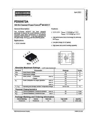
April 2001 FDS6672A 30V N-Channel PowerTrench MOSFET General Description Features This N-Channel MOSFET has been designed 12.5 A, 30 V. RDS(ON) = 8 m @ VGS = 10 V specifically to improve the overall efficiency of DC/DC RDS(ON) = 9.5 m @ VGS = 4.5 V converters using either synchronous or conventional switching PWM controllers. It has been optimized f
8.6. Size:226K fairchild semi
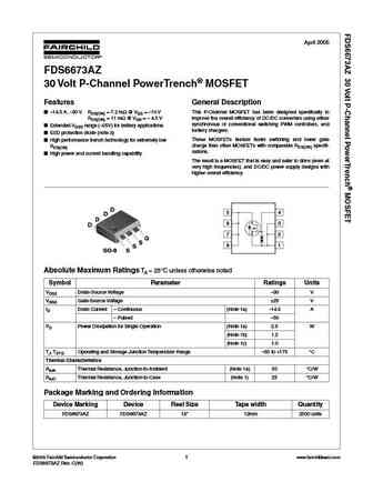
fds6673bz.pdf
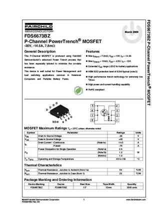
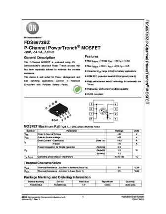
March 2009 FDS6673BZ P-Channel PowerTrench MOSFET -30V, -14.5A, 7.8m General Description Features This P-Channel MOSFET is produced using Fairchild Max rDS(on) = 7.8m , VGS = -10V, ID = -14.5A Semiconductor s advanced Power Trench process that Max rDS(on) = 12m , VGS = -4.5V, ID = -12A has been especially tailored to minimize the on-state Extended VGS range (-25V) for b
8.7. Size:63K fairchild semi
fds6679z.pdf
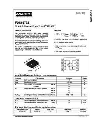
October 2001 FDS6679Z 30 Volt P-Channel PowerTrench MOSFET General Description Features This P-Channel MOSFET has been designed 13 A, 30 V. R = 9 m @ V = 10 V DS(ON) GS specifically to improve the overall efficiency of DC/DC R = 13 m @ V = 4.5 V DS(ON) GS converters using either synchronous or conventional switching PWM controllers, and battery charge
8.8. Size:479K fairchild semi
fds6679az.pdf
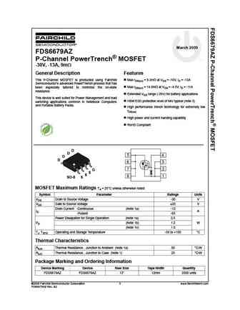
March 2009 FDS6679AZ tm P-Channel PowerTrench MOSFET -30V, -13A, 9m General Description Features This P-Channel MOSFET is producted using Fairchild Max rDS(on) = 9.3m at VGS = -10V, ID = -13A Semiconductor s advanced PowerTrench process that has Max rDS(on) = 14.8m at VGS = -4.5V, ID = -11A been especially tailored to minimize the on-state resistance. Extended VGS r
8.9. Size:199K fairchild semi
fds6675.pdf
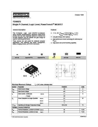
October 1998 FDS6675 Single P-Channel, Logic Level, PowerTrenchTM MOSFET General Description Features This P-Channel Logic Level MOSFET is produced -11 A, -30 V. RDS(ON) = 0.014 @ VGS = -10 V, using Fairchild Semiconductor's advanced PowerTrench RDS(ON) = 0.020 @ VGS = -4.5 V. process that has been especially tailored to minimize the Low gate charge (30nC typical). on-state
8.10. Size:137K fairchild semi
fds6670a.pdf
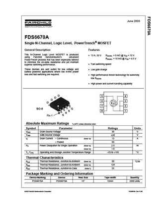
June 2003 FDS6670A Single N-Channel, Logic Level, PowerTrench MOSFET General Description Features This N-Channel Logic Level MOSFET is produced 13 A, 30 V. RDS(ON) = 8 m @ VGS = 10 V using Fairchild Semiconductor s advanced RDS(ON) = 10 m @ VGS = 4.5 V PowerTrench process that has been especially tailored to minimize the on-state resistance and yet maintain Fast switc
8.11. Size:600K fairchild semi
fds6673bz f085.pdf
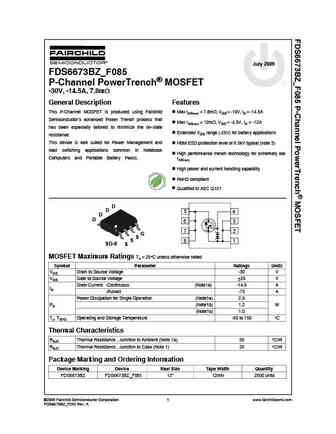
July 2009 FDS6673BZ_F085 P-Channel PowerTrench MOSFET -30V, -14.5A, 7.8m General Description Features This P-Channel MOSFET is produced using Fairchild Max rDS(on) = 7.8m , VGS = -10V, ID = -14.5A Semiconductor s advanced Power Trench process that Max rDS(on) = 12m , VGS = -4.5V, ID = -12A has been especially tailored to minimize the on-state Extended VGS range (-25V)
8.13. Size:321K onsemi
fds6670as.pdf

Is Now Part of To learn more about ON Semiconductor, please visit our website at www.onsemi.com Please note As part of the Fairchild Semiconductor integration, some of the Fairchild orderable part numbers will need to change in order to meet ON Semiconductor s system requirements. Since the ON Semiconductor product management systems do not have the ability to manage part nomenclatur
8.14. Size:447K onsemi
fds6675bz.pdf
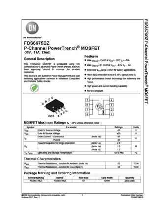
FDS6675BZ P-Channel PowerTrench MOSFET -30V, -11A, 13m Features General Description Max rDS(on) = 13m at VGS = -10V, ID = -11A This P-Channel MOSFET is producted using ON Max rDS(on) = 21.8m at VGS = -4.5V, ID = -9A Semiconductor s advanced PowerTrench process that has been especially tailored to minimize the on-state Extended VGS range (-25V) for battery application
8.15. Size:285K onsemi
fds6673bz.pdf
FDS6673BZ P-Channel PowerTrench MOSFET -30V, -14.5A, 7.8m Features General Description Max rDS(on) = 7.8m , VGS = -10V, ID = -14.5A This P-Channel MOSFET is produced using ON Semiconductor s advanced Power Trench process that Max rDS(on) = 12m , VGS = -4.5V, ID = -12A has been especially tailored to minimize the on-state Extended VGS range (-25V) for battery applicatio
8.16. Size:534K onsemi
fds6679az.pdf

Is Now Part of To learn more about ON Semiconductor, please visit our website at www.onsemi.com ON Semiconductor and the ON Semiconductor logo are trademarks of Semiconductor Components Industries, LLC dba ON Semiconductor or its subsidiaries in the United States and/or other countries. ON Semiconductor owns the rights to a number of patents, trademarks, copyrights, trade secrets, and oth
8.17. Size:282K onsemi
fds6675.pdf
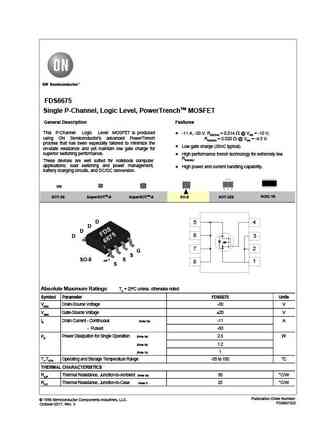
FDS6675 Single P-Channel, Logic Level, PowerTrenchTM MOSFET General Description Features This P-Channel Logic Level MOSFET is produced -11 A, -30 V. RDS(ON) = 0.014 @ VGS = -10 V, using ON Semiconductor's advanced PowerTrench RDS(ON) = 0.020 @ VGS = -4.5 V. process that has been especially tailored to minimize the Low gate charge (30nC typical). on-state resistance and yet
8.18. Size:250K onsemi
fds6670a.pdf

Is Now Part of To learn more about ON Semiconductor, please visit our website at www.onsemi.com Please note As part of the Fairchild Semiconductor integration, some of the Fairchild orderable part numbers will need to change in order to meet ON Semiconductor s system requirements. Since the ON Semiconductor product management systems do not have the ability to manage part nomenclatur
8.19. Size:1435K cn vbsemi
fds6670as.pdf
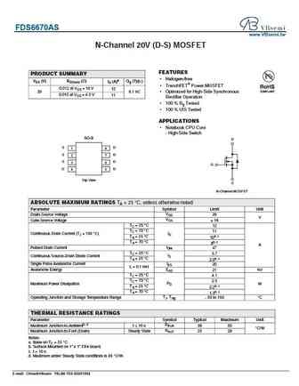
FDS6670AS www.VBsemi.tw N-Channel 20V (D-S) MOSFET FEATURES PRODUCT SUMMARY Halogen-free VDS (V) RDS(on) ( ) ID (A)a Qg (Typ.) TrenchFET Power MOSFET 0.012 at VGS = 10 V 12 20 6.1 nC Optimized for High-Side Synchronous 0.015 at VGS = 4.5 V 11 Rectifier Operation 100 % Rg Tested 100 % UIS Tested APPLICATIONS Notebook CPU Core - High-Side Switch S
8.20. Size:812K cn vbsemi
fds6673bz.pdf

FDS6673BZ www.VBsemi.tw P-Channel 30-V (D-S) MOSFET FEATURES PRODUCT SUMMARY Halogen-free VDS (V) RDS(on) ( ) ID (A)d Qg (Typ.) TrenchFET Power MOSFET 0.011 at VGS = - 10 V - 13.5 100 % Rg Tested RoHS - 30 29.5 nC COMPLIANT 100 % UIS Tested 0.015 at VGS = - 4.5 V - 11.6 APPLICATIONS Load Switch Notebook Adaptor Switch SO-8 S S 1 8 D S D 2 7 G
8.21. Size:814K cn vbsemi
fds6675b.pdf
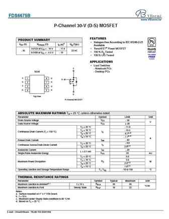
FDS6675B www.VBsemi.tw P-Channel 30-V (D-S) MOSFET FEATURES PRODUCT SUMMARY Halogen-free According to IEC 61249-2-21 VDS (V) RDS(on) ( ) ID (A)d Qg (Typ.) Available 0.0125 at VGS = - 10 V - 11.6 TrenchFET Power MOSFET - 30 22 nC 100 % Rg Tested 0.0180 at VGS = - 4.5 V - 10 100 % UIS Tested APPLICATIONS Load Switches S - Notebook PCs SO-8 - Desktop PCs
8.22. Size:811K cn vbsemi
fds6679az.pdf
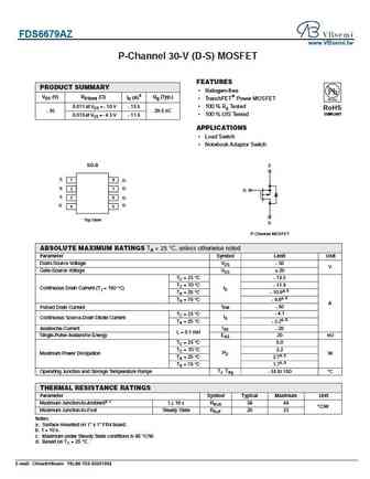
FDS6679AZ www.VBsemi.tw P-Channel 30-V (D-S) MOSFET FEATURES PRODUCT SUMMARY Halogen-free VDS (V) RDS(on) ( ) ID (A)d Qg (Typ.) TrenchFET Power MOSFET 0.011 at VGS = - 10 V - 13.5 100 % Rg Tested RoHS - 30 29.5 nC COMPLIANT 100 % UIS Tested 0.015 at VGS = - 4.5 V - 11.6 APPLICATIONS Load Switch Notebook Adaptor Switch SO-8 S S 1 8 D S D 2 7 G
Otros transistores... FDS6298
, STB31L01
, FDS6574A
, FDS6670AS
, STA6968
, FDS6673BZ
, FDS6673BZF085
, FDS6675BZ
, AO4468
, STA6620
, FDS6679AZ
, FDS6680AS
, STA6611
, FDS6681Z
, FDS6682
, STA6610
, FDS6690AS
.
History: FDS6673BZF085