NCE60P65K MOSFET Equivalente. Reemplazo. Hoja de especificaciones. Principales características
Número de Parte: NCE60P65K
Tipo de FET: MOSFET
Polaridad de transistor: P
ESPECIFICACIONES MÁXIMAS
Pdⓘ - Máxima
disipación de potencia: 130 W
|Vds|ⓘ - Voltaje máximo drenador-fuente: 60 V
|Vgs|ⓘ - Voltaje máximo fuente-puerta: 20 V
|Id|ⓘ - Corriente continua
de drenaje: 65 A
Tjⓘ - Temperatura máxima de unión: 175 °C
CARACTERÍSTICAS ELÉCTRICAS
trⓘ - Tiempo
de subida: 20 nS
Cossⓘ - Capacitancia de salida: 483 pF
RDSonⓘ - Resistencia estado encendido drenaje a fuente: 0.018 Ohm
Encapsulados: TO-252
Búsqueda de reemplazo de NCE60P65K MOSFET
- Selecciónⓘ de transistores por parámetros
NCE60P65K datasheet
..1. Size:638K ncepower
nce60p65k.pdf 
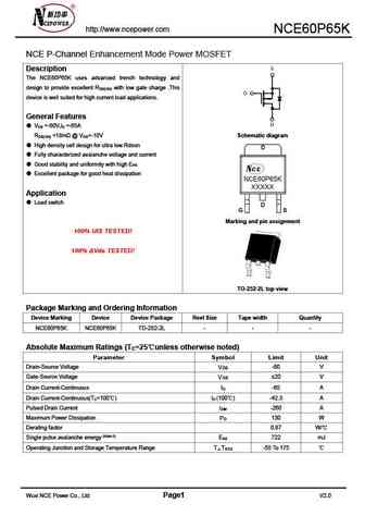
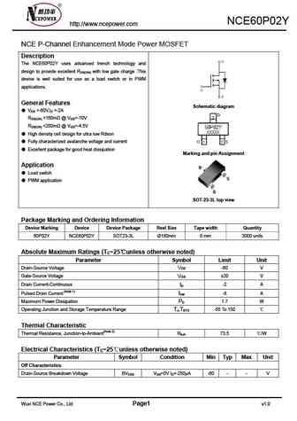
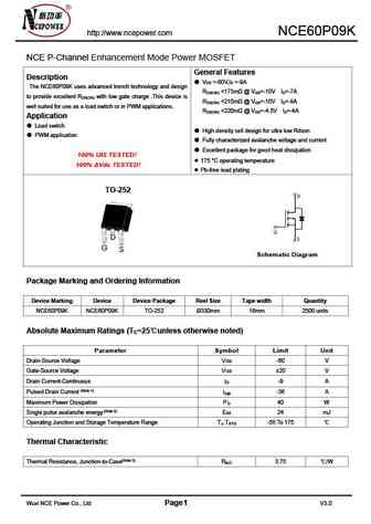
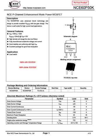
http //www.ncepower.com NCE60P65K NCE P-Channel Enhancement Mode Power MOSFET Description The NCE60P65K uses advanced trench technology and design to provide excellent R with low gate charge .This DS(ON) device is well suited for high current load applications. General Features V =-60V,I =-65A DS D R
8.1. Size:410K ncepower
nce60p16aq.pdf
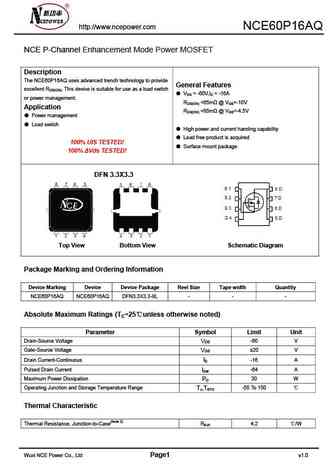
http //www.ncepower.com NCE60P16AQ NCE P-Channel Enhancement Mode Power MOSFET Description The NCE60P16AQ uses advanced trench technology to provide General Features excellent R , This device is suitable for use as a load switch DS(ON) V = -60V,I = -16A DS D or power management. R
8.3. Size:411K ncepower
nce60p05n.pdf
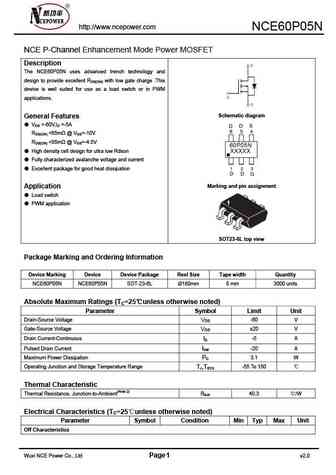
http //www.ncepower.com NCE60P05N NCE P-Channel Enhancement Mode Power MOSFET Description The NCE60P05N uses advanced trench technology and design to provide excellent RDS(ON) with low gate charge .This device is well suited for use as a load switch or in PWM applications. Schematic diagram General Features VDS =-60V,ID =-5A RDS(ON)
8.4. Size:356K ncepower
nce60p45ak.pdf
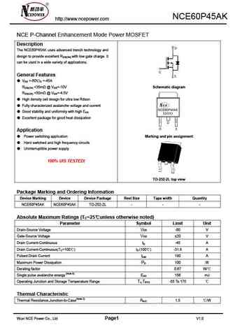
NCE60P45AK http //www.ncepower.com NCE P-Channel Enhancement Mode Power MOSFET Description The NCE60P45AK uses advanced trench technology and design to provide excellent RDS(ON) with low gate charge. It can be used in a wide variety of applications. General Features VDS =-60V,ID =-45A RDS(ON)
8.5. Size:364K ncepower
nce60p06s.pdf
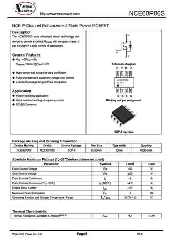
http //www.ncepower.com NCE60P06S NCE P-Channel Enhancement Mode Power MOSFET Description The NCE60P06S uses advanced trench technology and design to provide excellent RDS(ON) with low gate charge. It can be used in a wide variety of applications. General Features VDS =-60V,ID =-6A RDS(ON)
8.6. Size:351K ncepower
nce60p45k.pdf
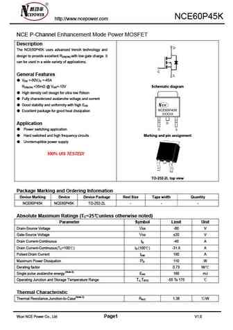
NCE60P45K http //www.ncepower.com NCE P-Channel Enhancement Mode Power MOSFET Description The NCE60P45K uses advanced trench technology and design to provide excellent RDS(ON) with low gate charge. It can be used in a wide variety of applications. General Features VDS =-60V,ID =-45A RDS(ON)
8.7. Size:282K ncepower
nce60p40f.pdf
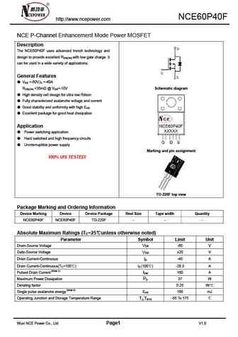
NCE60P40F http //www.ncepower.com NCE P-Channel Enhancement Mode Power MOSFET Description The NCE60P40F uses advanced trench technology and design to provide excellent RDS(ON) with low gate charge. It can be used in a wide variety of applications. General Features VDS =-60V,ID =-40A RDS(ON)
8.8. Size:611K ncepower
nce60p82ad.pdf
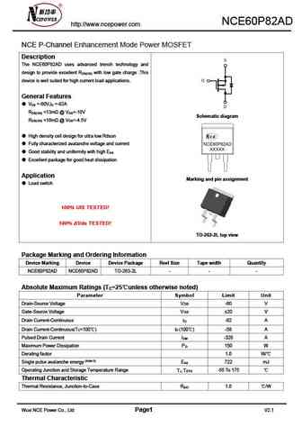
NCE60P82AD http //www.ncepower.com NCE P-Channel Enhancement Mode Power MOSFET Description The NCE60P82AD uses advanced trench technology and design to provide excellent R with low gate charge .This DS(ON) device is well suited for high current load applications. General Features V =-60V,I =-82A DS D R
8.9. Size:285K ncepower
nce60p09s.pdf
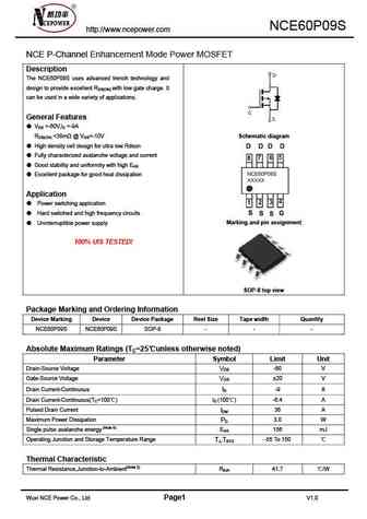
NCE60P09S http //www.ncepower.com NCE P-Channel Enhancement Mode Power MOSFET Description The NCE60P09S uses advanced trench technology and design to provide excellent RDS(ON) with low gate charge. It can be used in a wide variety of applications. General Features VDS =-60V,ID =-9A RDS(ON)
8.10. Size:627K ncepower
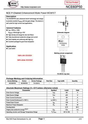
nce60p50g.pdf
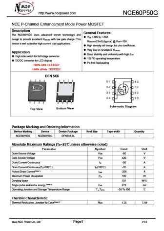
http //www.ncepower.com NCE60P50G NCE P-Channel Enhancement Mode Power MOSFET Description General Features The NCE60P50G uses advanced trench technology and V =-60V,I =-50A DS D design to provide excellent R with low gate charge .This DS(ON) R =23m (typical) @ V =-10V DS(ON) GS device is well suited for high current load applications. High density cell design for ultra lo
8.11. Size:347K ncepower
nce60p20k.pdf
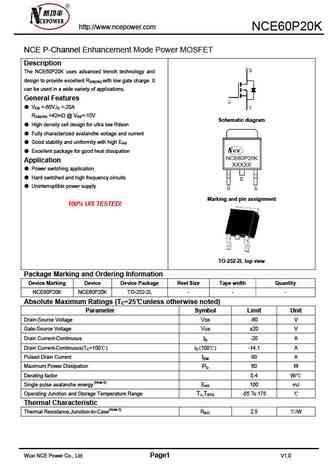
http //www.ncepower.com NCE60P20K NCE P-Channel Enhancement Mode Power MOSFET Description The NCE60P20K uses advanced trench technology and design to provide excellent RDS(ON) with low gate charge. It can be used in a wide variety of applications. General Features VDS =-60V,ID =-20A RDS(ON)
8.14. Size:683K ncepower
nce60p70d.pdf
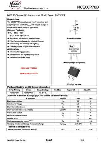
NCE60P70D http //www.ncepower.com NCE P-Channel Enhancement Mode Power MOSFET Description The NCE60P70D uses advanced trench technology and design to provide excellent R with low gate charge. It DS(ON) can be used in a wide variety of applications. General Features V =-60V,I =-70A DS D R
8.15. Size:624K ncepower
nce60p18aq.pdf
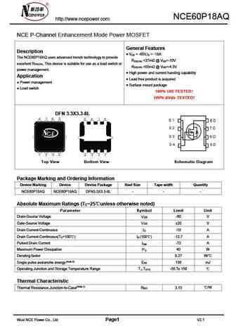
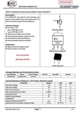
NCE60P18AQ http //www.ncepower.com NCE P-Channel Enhancement Mode Power MOSFET General Features Description V = -60V,I = -18A DS D The NCE60P18AQ uses advanced trench technology to provide R
8.17. Size:656K ncepower
nce60p03r.pdf
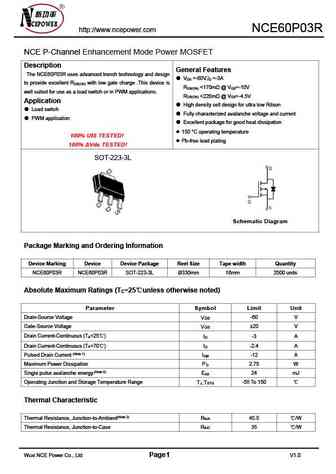
http //www.ncepower.com NCE60P03R NCE P-Channel Enhancement Mode Power MOSFET Description General Features The NCE60P03R uses advanced trench technology and design V =-60V,I =-3A DS D to provide excellent R with low gate charge .This device is DS(ON) R
8.18. Size:383K ncepower
nce60p28ak.pdf
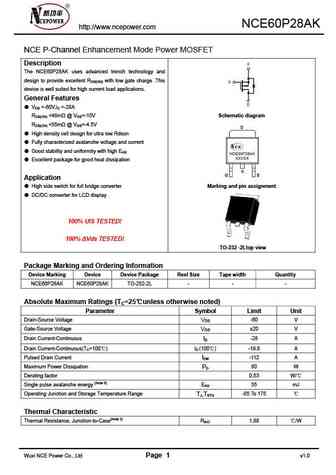
NCE60P28AK http //www.ncepower.com NCE P-Channel Enhancement Mode Power MOSFET Description The NCE60P28AK uses advanced trench technology and design to provide excellent RDS(ON) with low gate charge .This device is well suited for high current load applications. General Features VDS =-60V,ID =-28A RDS(ON)
8.19. Size:424K ncepower
nce60p10k.pdf
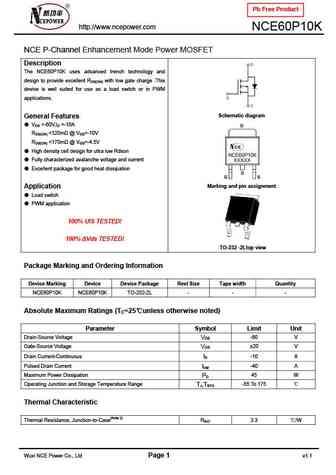
Pb Free Product http //www.ncepower.com NCE60P10K NCE P-Channel Enhancement Mode Power MOSFET Description The NCE60P10K uses advanced trench technology and design to provide excellent RDS(ON) with low gate charge .This device is well suited for use as a load switch or in PWM applications. Schematic diagram General Features VDS =-60V,ID =-10A RDS(ON)
8.21. Size:358K ncepower
nce60p25.pdf
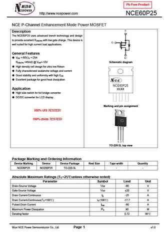
Pb Free Product http //www.ncepower.com NCE60P25 NCE P-Channel Enhancement Mode Power MOSFET Description The NCE60P25 uses advanced trench technology and design to provide excellent RDS(ON) with low gate charge .This device is well suited for high current load applications. General Features VDS =-60V,ID =-25A RDS(ON)
8.22. Size:358K ncepower
nce60p04sn.pdf
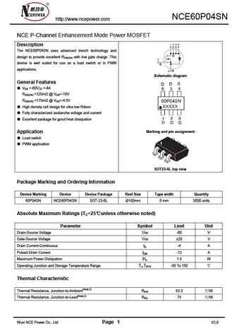
NCE60P04SN http //www.ncepower.com NCE P-Channel Enhancement Mode Power MOSFET Description The NCE60P04SN uses advanced trench technology and design to provide excellent RDS(ON) with low gate charge .This device is well suited for use as a load switch or in PWM applications. Schematic diagram General Features VDS =-60V,ID =-4A RDS(ON)
8.23. Size:288K ncepower
nce60p09as.pdf
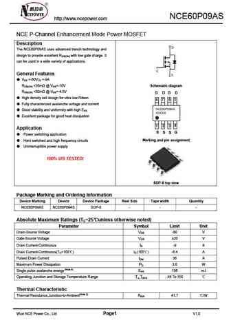
NCE60P09AS http //www.ncepower.com NCE P-Channel Enhancement Mode Power MOSFET Description The NCE60P09AS uses advanced trench technology and design to provide excellent RDS(ON) with low gate charge. It can be used in a wide variety of applications. General Features VDS =-60V,ID =-9A RDS(ON)
8.24. Size:303K ncepower
nce60p55k.pdf
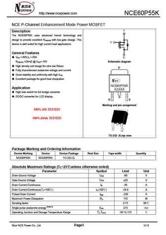
http //www.ncepower.com NCE60P55K NCE P-Channel Enhancement Mode Power MOSFET Description The NCE60P55K uses advanced trench technology and design to provide excellent RDS(ON) with low gate charge .This device is well suited for high current load applications. General Features VDS =-60V,ID =-55A RDS(ON)
8.25. Size:492K ncepower
nce60p05r.pdf
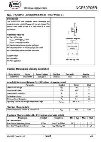
http //www.ncepower.com NCE60P05R NCE P-Channel Enhancement Mode Power MOSFET Description The NCE60P05R uses advanced trench technology and design to provide excellent RDS(ON) with low gate charge .This device is well suited for use as a load switch or in PWM applications. General Features VDS =-60V,ID =-5A Schematic diagram RDS(ON)
8.27. Size:675K ncepower
nce60p70g.pdf
http //www.ncepower.com NCE60P70G NCE P-Channel Enhancement Mode Power MOSFET Description General Features The NCE60P70G uses advanced trench technology and V =-60V,I =-70A DS D design to provide excellent R with low gate charge .This R =11m (typical) @ V =-10V DS(ON) DS(ON) GS device is well suited for high current load applications. R =13m (typical) @ V =-4.5V DS(ON) GS
8.28. Size:445K ncepower
nce60p12as.pdf
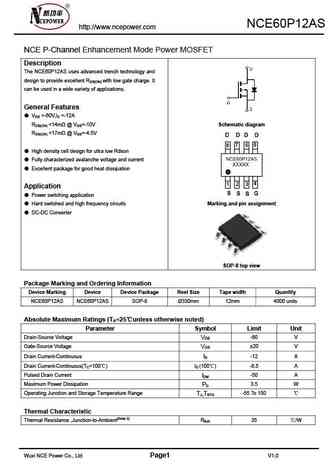
NCE60P12AS http //www.ncepower.com NCE P-Channel Enhancement Mode Power MOSFET Description The NCE60P12AS uses advanced trench technology and design to provide excellent RDS(ON) with low gate charge. It can be used in a wide variety of applications. General Features VDS =-60V,ID =-12A RDS(ON)
8.29. Size:788K ncepower
nce60p14k.pdf
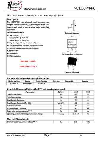
NCE60P14K http //www.ncepower.com NCE P-Channel Enhancement Mode Power MOSFET Description The NCE60P14K uses advanced trench technology and design to provide excellent R with low gate charge .This DS(ON) device is well suited for use as a load switch or in PWM applications. General Features Schematic diagram V =-60V,I =-14A DS D R
8.30. Size:371K ncepower
nce60p07as.pdf
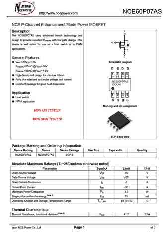
NCE60P07AS http //www.ncepower.com NCE P-Channel Enhancement Mode Power MOSFET Description The NCE60P07AS uses advanced trench technology and design to provide excellent RDS(ON) with low gate charge .This device is well suited for use as a load switch or in PWM applications. General Features VDS =-60V,ID =-7A Schematic diagram RDS(ON)
8.31. Size:655K ncepower
nce60p09k.pdf
http //www.ncepower.com NCE60P09K NCE P-Channel Enhancement Mode Power MOSFET General Features Description V =-60V,I =-9A DS D The NCE60P09K uses advanced trench technology and design R
8.32. Size:309K ncepower
nce60p50.pdf
Pb Free Product http //www.ncepower.com NCE60P50 NCE P-Channel Enhancement Mode Power MOSFET Description The NCE60P50 uses advanced trench technology and design to provide excellent RDS(ON) with low gate charge .This device is well suited for high current load applications. General Features VDS =-60V,ID =-50A RDS(ON)
8.33. Size:665K ncepower
nce60p82af.pdf
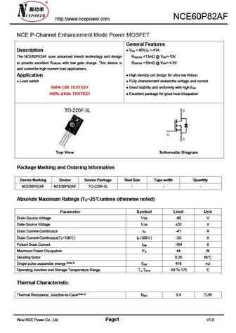
NCE60P82AF http //www.ncepower.com NCE P-Channel Enhancement Mode Power MOSFET General Features V =-60V,I =-41A Description DS D The NCE60P82AF uses advanced trench technology and design R
8.35. Size:397K ncepower
nce60p25k.pdf
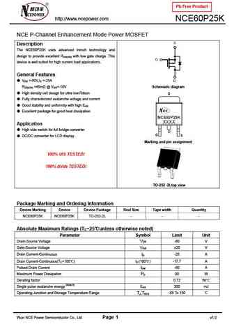
Pb Free Product http //www.ncepower.com NCE60P25K NCE P-Channel Enhancement Mode Power MOSFET Description The NCE60P25K uses advanced trench technology and design to provide excellent RDS(ON) with low gate charge .This device is well suited for high current load applications. General Features VDS =-60V,ID =-25A RDS(ON)
8.37. Size:360K ncepower
nce60pd05s.pdf

NCE60PD05S http //www.ncepower.com NCE P-Channel Enhancement Mode Power MOSFET Description D1 D2 The NCE60PD05S uses advanced trench technology and G1 G2 design to provide excellent RDS(ON) with low gate charge. It can be used in a wide variety of applications. S1 S2 Schematic diagram General Features VDS =-60V,ID =-5A RDS(ON)
8.38. Size:407K ncepower
nce60p50k.pdf
Pb Free Product http //www.ncepower.com NCE60P50K NCE P-Channel Enhancement Mode Power MOSFET Description The NCE60P50K uses advanced trench technology and design to provide excellent RDS(ON) with low gate charge .This device is well suited for high current load applications. General Features VDS =-60V,ID =-50A RDS(ON)
8.39. Size:344K ncepower
nce60p04y.pdf
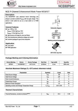
Pb Free Product http //www.ncepower.com NCE60P04Y NCE P-Channel Enhancement Mode Power MOSFET Description The NCE60P04Y uses advanced trench technology and design to provide excellent RDS(ON) with low gate charge .This device is well suited for use as a load switch or in PWM applications. General Features Schematic diagram VDS =-60V,ID =-4A RDS(ON)
8.40. Size:353K ncepower
nce60p03y.pdf
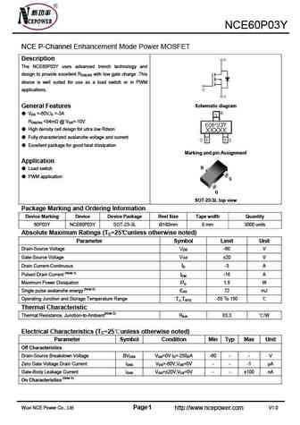
NCE60P03Y NCE P-Channel Enhancement Mode Power MOSFET Description The NCE60P03Y uses advanced trench technology and design to provide excellent RDS(ON) with low gate charge .This device is well suited for use as a load switch or in PWM applications. Schematic diagram General Features VDS =-60V,ID =-3A RDS(ON)
8.41. Size:711K ncepower
nce60p17aq.pdf
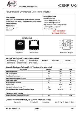
NCE60P17AQ http //www.ncepower.com NCE P-Channel Enhancement Mode Power MOSFET General Features Description V = -60V,I = -17A DS D The NCE60P17AQ uses advanced trench technology to provide R
8.42. Size:333K ncepower
nce60p04r.pdf
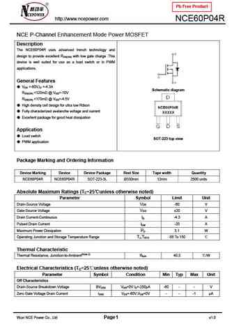
Pb Free Product http //www.ncepower.com NCE60P04R NCE P-Channel Enhancement Mode Power MOSFET Description The NCE60P04R uses advanced trench technology and design to provide excellent RDS(ON) with low gate charge .This device is well suited for use as a load switch or in PWM applications. General Features VDS =-60V,ID =-4.3A Schematic diagram RDS(ON)
8.43. Size:624K ncepower
nce60p82ak.pdf
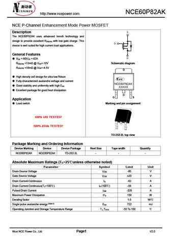
NCE60P82AK http //www.ncepower.com NCE P-Channel Enhancement Mode Power MOSFET Description The NCE60P82AK uses advanced trench technology and design to provide excellent R with low gate charge .This DS(ON) device is well suited for high current load applications. General Features V =-60V,I =-82A DS D R
8.44. Size:805K cn vbsemi
nce60p25k.pdf
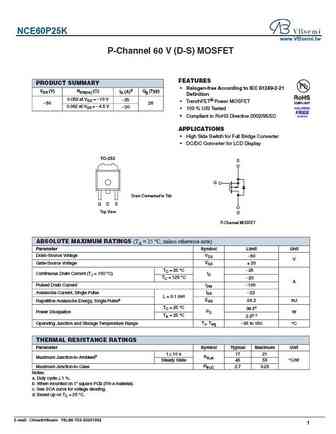
NCE60P25K www.VBsemi.tw P-Channel 60 V (D-S) MOSFET FEATURES PRODUCT SUMMARY Halogen-free According to IEC 61249-2-21 VDS (V) RDS(on) ( ) ID (A)d Qg (Typ) Definition 0.053 at VGS = - 10 V - 25 TrenchFET Power MOSFET - 60 26 0.062 at VGS = - 4.5 V - 20 100 % UIS Tested Compliant to RoHS Directive 2002/95/EC APPLICATIONS High Side Switch for Full Bri
Otros transistores... NCE60P16AQ, NCE60P17AQ, NCE60P18AQ, NCE60P25, NCE60P28AK, NCE60P40F, NCE60P45AK, NCE60P50G, IRF1405, NCE60P70D, NCE60P70G, NCE60P82A, NCE60P82AD, NCE60P82AK, NCE60PD05S, NCE60T2K2I, NCE60T2K2K