IRFW630B MOSFET Equivalente. Reemplazo. Hoja de especificaciones. Principales características
Número de Parte: IRFW630B
Tipo de FET: MOSFET
Polaridad de transistor: N
ESPECIFICACIONES MÁXIMAS
Pdⓘ - Máxima disipación de potencia: 72 W
|Vds|ⓘ - Voltaje máximo drenador-fuente: 200 V
|Vgs|ⓘ - Voltaje máximo fuente-puerta: 30 V
|Id|ⓘ - Corriente continua de drenaje: 9 A
Tjⓘ - Temperatura máxima de unión: 150 °C
CARACTERÍSTICAS ELÉCTRICAS
RDSonⓘ - Resistencia estado encendido drenaje a fuente: 0.4 Ohm
Búsqueda de reemplazo de IRFW630B MOSFET
- Selecciónⓘ de transistores por parámetros
IRFW630B datasheet
irfw630b irfi630b.pdf
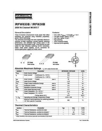
IRFW630B / IRFI630B 200V N-Channel MOSFET General Description Features These N-Channel enhancement mode power field effect 9.0A, 200V, RDS(on) = 0.4 @VGS = 10 V transistors are produced using Fairchild s proprietary, Low gate charge ( typical 22 nC) planar, DMOS technology. Low Crss ( typical 22 pF) This advanced technology has been especially tailored to Fast switc
irfw630b.pdf
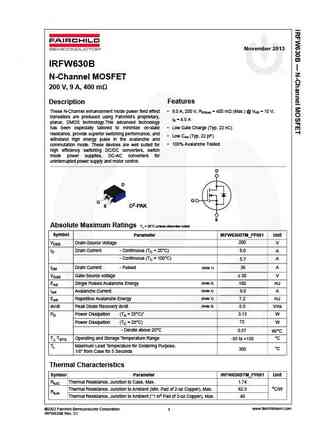
November 2013 IRFW630B N-Channel MOSFET 200 V, 9 A, 400 m Features Description These N-Channel enhancement mode power field effect 9.0 A, 200 V, RDS(on) = 400 m (Max.) @ VGS = 10 V, transistors are produced using Fairchild s proprietary, ID = 4.5 A planar, DMOS technology.This advanced technology has been especially tailored to minimize on-state Low Gate Charge (Typ.
irfw630a.pdf
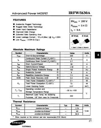
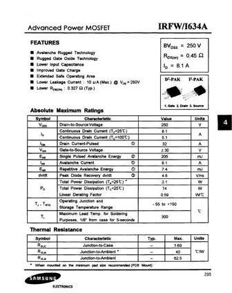
Advanced Power MOSFET FEATURES BVDSS = 200 V Avalanche Rugged Technology RDS(on) = 0.4 Rugged Gate Oxide Technology Lower Input Capacitance ID = 9 A Improved Gate Charge Extended Safe Operating Area Lower Leakage Current 10 A (Max.) @ VDS = 200V 2 Low RDS(ON) 0.333 (Typ.) 1 1 2 3 3 1. Gate 2. Drain 3. Source Absolute Maximum Ratings Symbol Charact
Otros transistores... FQD9N25TMF085 , FQH44N10 , FDS4480 , FQH8N100C , FQI13N50C , FQI27N25 , FQI27N25TUF085 , FQI4N80 , IRF640 , FQI4N90 , FQI50N06 , FQI5N60C , IRF644B , FQI7N60 , IRF634B , FQI7N80 , FDC6392S .
🌐 : EN ES РУ

Liste
Recientemente añadidas las descripciónes de los transistores:
MOSFET: AUB062N08BG | AUB060N08AG | AUB056N10 | AUB056N08BGL | AUB050N085 | AUB050N055 | AUB045N12 | AUB045N10BT | AUB039N10 | AUB034N10 | AUB033N08BG | AUB026N085 | AUA062N08BG | AUA060N08AG | AUA056N08BGL | AUA039N10
Popular searches
irf840 datasheet | ge10001 | irf830 | irfp450 | mj21193 | s9014 transistor | bc547 transistor datasheet | c945 datasheet