FIR11NS65AFG MOSFET Equivalente. Reemplazo. Hoja de especificaciones. Principales características
Número de Parte: FIR11NS65AFG
Tipo de FET: MOSFET
Polaridad de transistor: N
ESPECIFICACIONES MÁXIMAS
Pdⓘ - Máxima disipación de potencia: 35 W
|Vds|ⓘ - Voltaje máximo drenador-fuente: 650 V
|Vgs|ⓘ - Voltaje máximo fuente-puerta: 30 V
|Id|ⓘ - Corriente continua de drenaje: 11 A
Tjⓘ - Temperatura máxima de unión: 150 °C
CARACTERÍSTICAS ELÉCTRICAS
trⓘ - Tiempo de subida: 35 nS
Cossⓘ - Capacitancia de salida: 37 pF
RDSonⓘ - Resistencia estado encendido drenaje a fuente: 0.4 Ohm
Encapsulados: TO-220F
Búsqueda de reemplazo de FIR11NS65AFG MOSFET
- Selecciónⓘ de transistores por parámetros
FIR11NS65AFG datasheet
fir11ns65afg.pdf
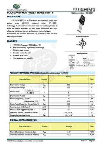
FIR11NS65AFG 11A, 650V DP MOS POWER TRANSISTOR-S PIN Connection TO-220F DESCRIPTION FIR11NS65AFG is an N-channel enhancement mode high voltage power MOSFETs produced using DP MOS technology. It achieves low conduction loss and switching losses. It leads the design engineers to their power converters with high G efficiency, high power density, and superior thermal behavior. D S
fir11ns70afg.pdf
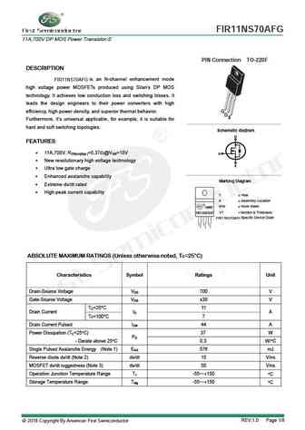
FIR11NS70AFG 11A,700V DP MOS Power Transistor-S PIN Connection TO-220F DESCRIPTION FIR11NS70AFG is an N-channel enhancement mode high voltage power MOSFETs produced using Silan s DP MOS technology. It achieves low conduction loss and switching losses. It leads the design engineers to their power converters with high efficiency, high power density, and superior thermal behavior. G
fir11n90ang.pdf
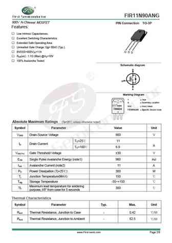
FIR11N90ANG 900V N-Channel MOSFET PIN Connection TO-3P Features Low Intrinsic Capacitances. Excellent Switching Characteristics. Extended Safe Operating Area. Unrivalled Gate Charge Qg= 60nC (Typ.). BVDSS=900V,ID=11A RDS(on) 1.1 (Max) @VG=10V 100% Avalanche Tested g Schematic dia ram D G S Marking Diagram Y = Year A = Assembly Location
fir11n40fg.pdf
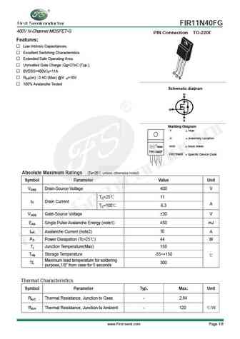
FIR11N40FG 400V N-Channel MOSFET-G PIN Connection TO-220F Features Low Intrinsic Capacitances. Excellent Switching Characteristics. Extended Safe Operating Area. Unrivalled Gate Charge Qg=27nC (Typ.). BVDSS=400V,ID=11A G DS RDS(on) 0.4 (Max) @V =10V G 100% Avalanche Tested g Schematic dia ram D G S Marking Diagram Y = Year A = Assembly Loc
Otros transistores... FIR10N10LG, FIR10N20LG, FIR10N50FG, FIR10N70FG, FIR10N80FG, FIR110N10PG, FIR11N40FG, FIR11N90ANG, IRF640, FIR11NS70AFG, FIR120N08PG, FIR12N15LG, FIR12N70FG, FIR12N80FG, FIR13N50FG, FIR14N50FG, FIR14N65FG
🌐 : EN ES РУ

Liste
Recientemente añadidas las descripciónes de los transistores:
MOSFET: CM4407 | CM3407 | CM3400 | SVF11N65F | SVF11N65T | FKBB3105 | EHBA036R1 | CRTT067N10N | AP6NA3R2MT | AP65SA145DDT8 | AP4NAR95CMT-A | AP4024GEMT-HF | AP3P050AH | AP3P020H | AP3N9R5YT | AP3N9R5MT
Popular searches
c2026 | mpsa56 transistor equivalent | 13009 transistor | irf3205 equivalent | ksa992 transistor | 2n2926 | ksa992 pinout | 2n1308 transistor