D5N50 Datasheet. Equivalente. Reemplazo. Hoja de especificaciones. Principales características
Número de Parte: D5N50 📄📄
Tipo de FET: MOSFET
Polaridad de transistor: N
ESPECIFICACIONES MÁXIMAS
Pdⓘ - Máxima disipación de potencia: 74 W
|Vds|ⓘ - Voltaje máximo drenador-fuente: 500 V
|Vgs|ⓘ - Voltaje máximo fuente-puerta: 30 V
|Id|ⓘ - Corriente continua de drenaje: 5 A
Tjⓘ - Temperatura máxima de unión: 150 °C
CARACTERÍSTICAS ELÉCTRICAS
trⓘ - Tiempo de subida: 25 nS
Cossⓘ - Capacitancia de salida: 45 pF
RDSonⓘ - Resistencia estado encendido drenaje a fuente: 1.5 Ohm
Encapsulados: TO252
📄📄 Copiar
Búsqueda de reemplazo de D5N50 MOSFET
- Selecciónⓘ de transistores por parámetros
D5N50 datasheet
..1. Size:642K cn wxdh
d5n50 b5n50.pdf 
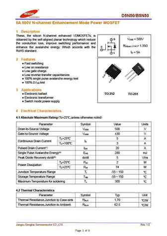
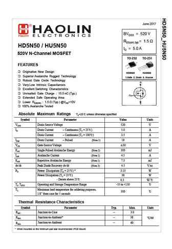
D5N50/B5N50 5A 500V N-channel Enhancement Mode Power MOSFET 1 Description These, the silicon N-channel enhanced VDMOSFETs, is 2 D V = 500V DSS obtained by the self-aligned planar technology which reduce the conduction loss, improve switching performance and R = 1.35 DS(on) (TYP) G enhance the avalanche energy. Which accords with the 1 RoHS standard. I = 5A 3 S D 2
0.1. Size:645K fairchild semi
fdd5n50u.pdf

December 2007 TM Ultra FRFET FDD5N50U tm N-Channel MOSFET, FRFET 500V, 3A, 2.0 Features Description RDS(on) = 1.65 ( Typ.)@ VGS = 10V, ID = 1.5A These N-Channel enhancement mode power field effect transis- tors are produced using Fairchild s proprietary, planar stripe, Low gate charge ( Typ. 11nC) DOMS technology. Low Crss ( Typ. 5pF) This advance technology h
0.2. Size:548K fairchild semi
fqd5n50.pdf
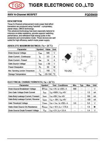
TIGER ELECTRONIC CO.,LTD 500V N-Channel MOSFET FQD5N50 DESCRIPTION These N-Channel enhancement mode power field effect transistors are produced using Fairchild s proprietary, planar stripe, DMOS technology. This advanced technology has been especially tailored to minimize on-state resistance, provide superior switching performance, and withstand high energy pulse in the avalanche an
0.3. Size:752K fairchild semi
fdd5n50f.pdf
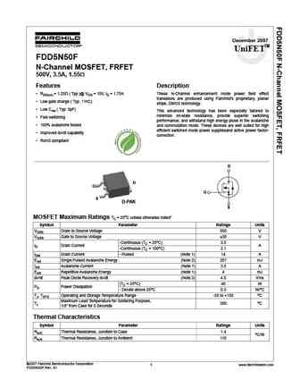
December 2007 UniFETTM FDD5N50F tm N-Channel MOSFET, FRFET 500V, 3.5A, 1.55 Features Description RDS(on) = 1.25 ( Typ.)@ VGS = 10V, ID = 1.75A These N-Channel enhancement mode power field effect transistors are produced using Fairchild s proprietary, planar Low gate charge ( Typ. 11nC) stripe, DMOS technology. Low Crss ( Typ. 5pF) This advanced technology has
0.4. Size:503K fairchild semi
fdd5n50.pdf
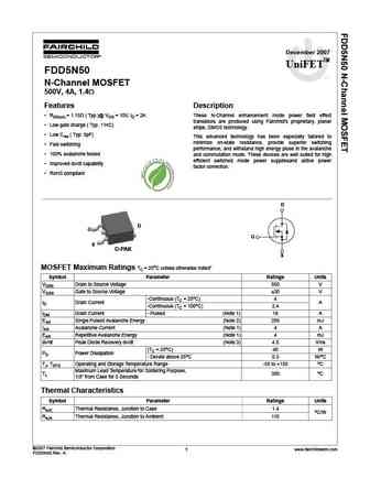
December 2007 UniFETTM FDD5N50 tm N-Channel MOSFET 500V, 4A, 1.4 Features Description RDS(on) = 1.15 ( Typ.)@ VGS = 10V, ID = 2A These N-Channel enhancement mode power field effect transistors are produced using Fairchild s proprietary, planar Low gate charge ( Typ. 11nC) stripe, DMOS technology. Low Crss ( Typ. 5pF) This advanced technology has been especiall
0.5. Size:664K fairchild semi
fqd5n50c fqd5n50ctf fqd5n50ctm fqd5n50c fqu5n50c fqu5n50ctu.pdf
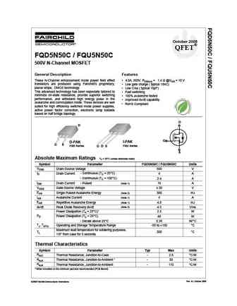
October 2008 QFET FQD5N50C / FQU5N50C 500V N-Channel MOSFET General Description Features These N-Channel enhancement mode power field effect 4.0A, 500V, RDS(on) = 1.4 @VGS = 10 V transistors are produced using Fairchild s proprietary, Low gate charge ( typical 18nC) planar stripe, DMOS technology. Low Crss ( typical 15pF) This advanced technology has been especially
0.6. Size:768K fairchild semi
fqd5n50tf fqu5n50tu.pdf
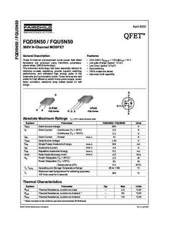
April 2000 TM QFET QFET QFET QFET 500V N-ChanneI MOSFET GeneraI Description Features These N-Channel enhancement mode power field effect 3.5A, 500V, RDS(on) = 1.8 @VGS = 10 V transistors are produced using Fairchild s proprietary, Low gate charge ( typical 13 nC) planar stripe, DMOS technology. Low Crss ( typical 8.5 pF) This advanced technology
0.7. Size:548K fairchild semi
fdd5n50nz.pdf

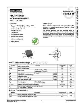
November 2009 UniFET-IITM FDD5N50NZ N-Channel MOSFET 500V, 4A, 1.5 Features Description RDS(on) = 1.38 ( Typ.)@ VGS = 10V, ID = 2A These N-Channel enhancement mode power field effect transistors are produced using Fairchild s proprietary, planar Low Gate Charge ( Typ. 9nC) stripe, DMOS technology. Low Crss ( Typ. 4pF) This advance technology has been especially
0.8. Size:564K fairchild semi
fdd5n50nzf.pdf
November 2009 UniFET-IITM FDD5N50NZF N-Channel MOSFET 500V, 3.7A, 1.75 Features Description RDS(on) = 1.47 ( Typ.)@ VGS = 10V, ID = 1.85A These N-Channel enhancement mode power field effect transistors are produced using Fairchild s proprietary, planar Low Gate Charge ( Typ. 9nC) stripe, DMOS technology. Low Crss ( Typ. 4pF) This advance technology has been esp
0.9. Size:198K vishay
sihd5n50d.pdf
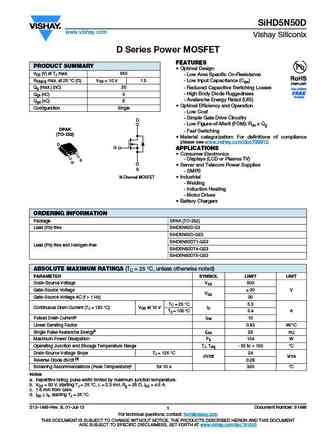
SiHD5N50D www.vishay.com Vishay Siliconix D Series Power MOSFET FEATURES PRODUCT SUMMARY Optimal Design VDS (V) at TJ max. 550 - Low Area Specific On-Resistance RDS(on) max. at 25 C ( ) VGS = 10 V 1.5 - Low Input Capacitance (Ciss) Qg (max.) (nC) 20 - Reduced Capacitive Switching Losses - High Body Diode Ruggedness Qgs (nC) 3 Available - Avalanche Energy Rated (UIS) Qgd
0.10. Size:833K onsemi
fdd5n50u.pdf
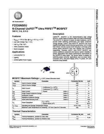
FDD5N50U N-Channel UniFETTM Ultra FRFETTM MOSFET 500 V, 3 A, 2.0 Description Features UniFETTM MOSFET is ON Semiconductor s high voltage MOSFET family based on planar stripe and DMOS technology. RDS(on) = 1.65 (Typ.) @ VGS = 10 V, ID = 1.5 A This MOSFET is tailored to reduce on-state resistance, and to Low Gate Charge (Typ. 11 nC) provide better switching performance
0.11. Size:841K onsemi
fdd5n50.pdf
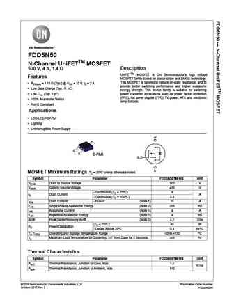
FDD5N50 N-Channel UniFETTM MOSFET Description 500 V, 4 A, 1.4 UniFETTM MOSFET is ON Semiconductor s high voltage Features MOSFET family based on planar stripe and DMOS technology. This MOSFET is tailored to reduce on-state resistance, and to RDS(on) = 1.15 (Typ.) @ VGS = 10 V, ID = 2 A provide better switching performance and higher avalanche Low Gate Charge (Typ.
0.12. Size:765K onsemi
fdd5n50ftm-ws.pdf
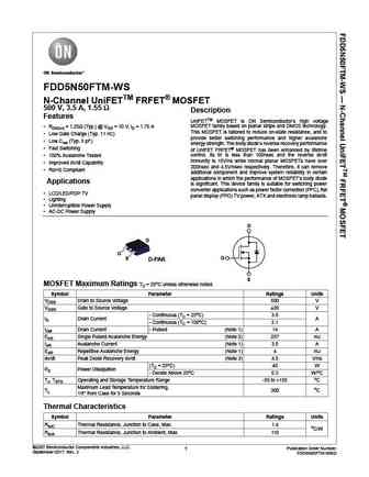
FDD5N50FTM-WS N-Channel UniFETTM FRFET MOSFET 500 V, 3.5 A, 1.55 Description Features UniFETTM MOSFET is ON Semiconductor s high voltage RDS(on) = 1.25 (Typ.) @ VGS = 10 V, ID = 1.75 A MOSFET family based on planar stripe and DMOS technology. This MOSFET is tailored to reduce on-state resistance, and to Low Gate Charge (Typ. 11 nC) provide better switching performa
0.13. Size:713K onsemi
fdd5n50nz.pdf

Is Now Part of To learn more about ON Semiconductor, please visit our website at www.onsemi.com Please note As part of the Fairchild Semiconductor integration, some of the Fairchild orderable part numbers will need to change in order to meet ON Semiconductor s system requirements. Since the ON Semiconductor product management systems do not have the ability to manage part nomenclatur
0.15. Size:284K aosemi
aod5n50.pdf
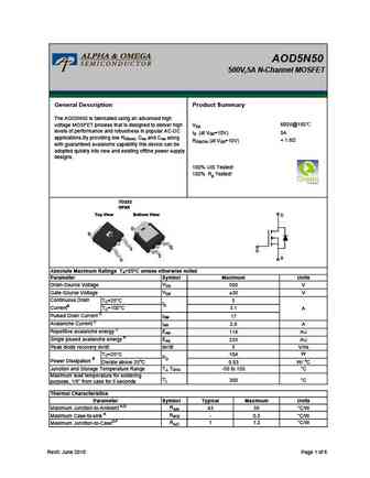
AOD5N50 500V,5A N-Channel MOSFET General Description Product Summary The AOD5N50 is fabricated using an advanced high 600V@150 voltage MOSFET process that is designed to deliver high VDS levels of performance and robustness in popular AC-DC ID (at VGS=10V) 5A applications.By providing low RDS(on), Ciss and Crss along
0.16. Size:979K blue-rocket-elect
brd5n50.pdf
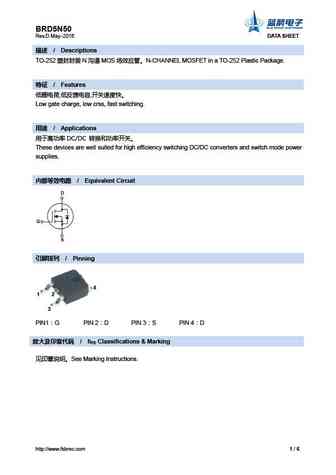
BRD5N50 Rev.D May.-2016 DATA SHEET / Descriptions TO-252 N MOS N-CHANNEL MOSFET in a TO-252 Plastic Package. / Features , , Low gate charge, low crss, fast switching. / Applications DC/DC These devices are well suited for high efficiency switching
0.17. Size:928K magnachip
mdd5n50frh.pdf
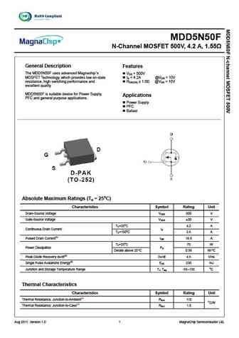
MDD5N50F N-Channel MOSFET 500V, 4.2 A, 1.55 General Description Features The MDD5N50F uses advanced Magnachip s V = 500V DS MOSFET Technology, which provides low on-state I = 4.2A @V = 10V D GS resistance, high switching performance and RDS(ON) 1.5 @VGS = 10V excellent quality. MDD5N50F is suitable device for Power Supply, Applications PFC and gen
0.18. Size:770K magnachip
mdd5n50zrh.pdf
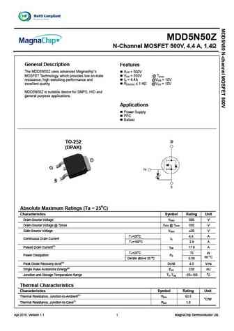
MDD5N50Z N-Channel MOSFET 500V, 4.4 A, 1.4 General Description Features The MDD5N50Z uses advanced Magnachip s V = 500V DS MOSFET Technology, which provides low on-state VDS = 550V @ Tjmax resistance, high switching performance and I = 4.4A @V = 10V D GS excellent quality. R 1.4 @V = 10V DS(ON) GS MDD5N50Z is suitable device for SMPS, HID and general pur
0.19. Size:919K magnachip
mdd5n50rh.pdf

MDD5N50 N-Channel MOSFET 500V, 4.4 A, 1.4 General Description Features The MDD5N50 uses advanced Magnachip s V = 500V DS MOSFET Technology, which provides low on-state I = 4.4A @V = 10V D GS resistance, high switching performance and RDS(ON) 1.4 @VGS = 10V excellent quality. MDD5N50 is suitable device for SMPS, Ballast and general purpose applicatio
0.20. Size:734K winsemi
wfd5n50.pdf
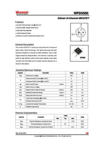
WFD5N50 WFD5N50 WFD5N50 WFD5N50 Silicon N-Channel MOSFET Silicon N-Channel MOSFET Silicon N-Channel MOSFET Silicon N-Channel MOSFET Features 5A,500V,RDS(on)(Max1.6 )@VGS=10V Ultra-low Gate Charge(Typical 32nC) Fast Switching Capability 100%Avalanche Tested Maximum Junction Temperature Range(150 ) General Description This Power MO SFET is pro du ced using Wi
0.21. Size:319K maple semi
sld5n50s2 slu5n50s2.pdf
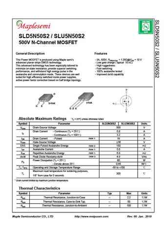
LEAD FREE Pb RoHS SLD5N50S2 / SLU5N50S2 500V N-Channel MOSFET General Description Features This Power MOSFET is produced using Maple semi s - 5A, 500V, RDS(on) typ. = 1.35 @VGS = 10 V ( ) yp advanced planar stripe DMOS technology. - Low gate charge ( typical 10 nC) This advanced technology has been especially tailored to - High ruggedness minimize on-state resistance, provide super
0.22. Size:276K semihow
hfd5n50s.pdf
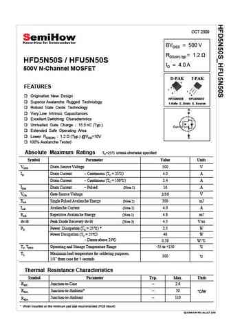
OCT 2009 BVDSS = 500 V RDS(on) typ HFD5N50S / HFU5N50S ID = 4.0 A 500V N-Channel MOSFET D-PAK I-PAK 2 FEATURES 1 1 3 2 3 Originative New Design HFD5N50S HFU5N50S Superior Avalanche Rugged Technology 1.Gate 2. Drain 3. Source Robust Gate Oxide Technology Very Low Intrinsic Capacitances Excellent Switching Characteristics Unrivalled Gate Charge 15.5 nC
0.23. Size:276K semihow
hfd5n50s hfu5n50s.pdf

OCT 2009 BVDSS = 500 V RDS(on) typ HFD5N50S / HFU5N50S ID = 4.0 A 500V N-Channel MOSFET D-PAK I-PAK 2 FEATURES 1 1 3 2 3 Originative New Design HFD5N50S HFU5N50S Superior Avalanche Rugged Technology 1.Gate 2. Drain 3. Source Robust Gate Oxide Technology Very Low Intrinsic Capacitances Excellent Switching Characteristics Unrivalled Gate Charge 15.5 nC
0.24. Size:207K semihow
hfd5n50u.pdf

Jan 2014 BVDSS = 500 V RDS(on) typ HFD5N50U / HFU5N50U ID = 4.0 A 500V N-Channel MOSFET D-PAK I-PAK FEATURES 2 1 Originative New Design 1 3 2 3 Superior Avalanche Rugged Technology HFD5N50U HFU5N50U Robust Gate Oxide Technology 1.Gate 2. Drain 3. Source Very Low Intrinsic Capacitances Excellent Switching Characteristics Unrivalled Gate Charge 13 nC (
0.25. Size:287K semihow
hfd5n50u hfu5n50u.pdf
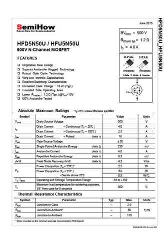
June 2015 BVDSS = 500 V RDS(on) typ HFD5N50U / HFU5N50U ID = 4.0 A 500V N-Channel MOSFET D-PAK I-PAK FEATURES 2 1 Originative New Design 1 3 2 3 Superior Avalanche Rugged Technology HFD5N50U HFU5N50U Robust Gate Oxide Technology 1.Gate 2. Drain 3. Source Very Low Intrinsic Capacitances Excellent Switching Characteristics Unrivalled Gate Charge 13 nC
0.26. Size:661K taitron
msu4d5n50q.pdf
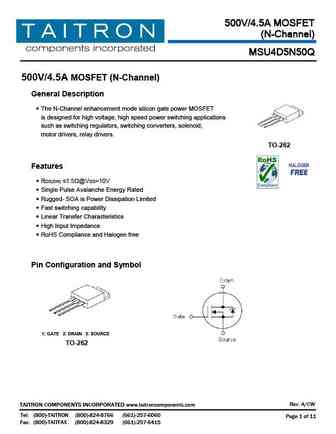
500V/4.5A MOSFET (N-Channel) MSU4D5N50Q 500V/4.5A MOSFET (N-Channel) General Description The N-Channel enhancement mode silicon gate power MOSFET is designed for high voltage, high speed power switching applications such as switching regulators, switching converters, solenoid, motor drivers, relay drivers. TO-262 Features RDS(ON) 1.5 @VGS=10V Single Pul
0.27. Size:345K trinnotech
tmd5n50 tmd5n50g tmu5n50 tmu5n50g.pdf
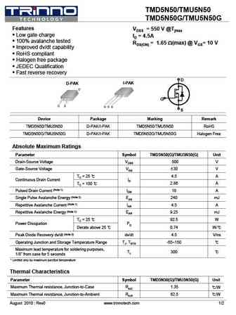
TMD5N50/TMU5N50 TMD5N50G/TMU5N50G Features VDSS = 550 V @Tjmax Low gate charge ID = 4.5A 100% avalanche tested RDS(ON) = 1.65 W(max) @ VGS= 10 V Improved dv/dt capability RoHS compliant Halogen free package JEDEC Qualification Fast reverse recovery D I-PAK D-PAK G S Device Package Marking Remark TMD5N50/TMU5N50 D-PAK/I-PAK TMD5N50/TMU5N50 RoHS
0.28. Size:800K truesemi
tsd5n50mr.pdf
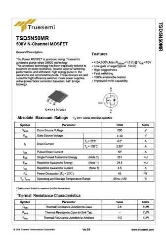
TSD5N50MR 500V N-Channel MOSFET General Description Features This Power MOSFET is produced using Truesemi s 4.5A,500V,Max.RDS(on)=1.6 @ VGS =10V advanced planar stripe DMOS technology. This advanced technology has been especially tailored to Low gate charge(typical 12nC) minimize on-state resistance, provide superior switching High ruggedness performance, an
0.29. Size:731K fortior tech
fmd5n50e5.pdf
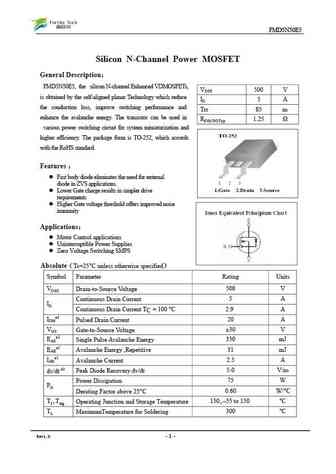
FMD5N50E5 Silicon N-Channel Power MOSFET General Description FMD5N50E5, the silicon N-channel Enhanced VDMOSFETs, VDSS 500 V is obtained by the self-aligned planar Technology which reduce ID 5 A the conduction loss, improve switching performance and Trr 85 ns enhance the avalanche energy. The transistor can be used in RDS(ON)Typ 1.25 various power switching circuit
0.31. Size:1205K lonten
lnc5n50 lnd5n50 lng5n50 lnh5n50.pdf
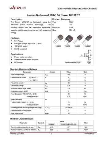
LNC5N50 LND5N50 LNG5N50 LNH5N50 Lonten N-channel 500V, 5A Power MOSFET Description Product Summary The Power MOSFET is fabricated using the V 500V DSS advanced planar VDMOS technology. The I 5A D resulting device has low conduction resistance, R 1.6 DS(on),max superior switching performance and high avalanche Q 12.8 nC g,typ energy. Features Low R DS(on) Low gate charge
0.32. Size:925K cn sinai power
spd5n50g.pdf
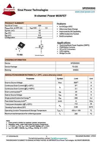
SPD5N50G Sinai Power Technologies www.sinai-power.com N-channel Power MOSFET PRODUCT SUMMARY Features V (V) at T max. 550 DS J ID=5A(Vgs=10V) R max. at 25oC ( ) V =10V 1.5 DS(on) GS Ultra Low Gate Charge Q max. (nC) 42 g Improved dv/dt Capability Q (nC) 12 gs 100% Avalanche Tested Q (nC) 6.5 gd RoHS compliant Configuration single Ap
0.33. Size:601K cn marching-power
mpvu5n50ccfd mpvd5n50ccfd.pdf
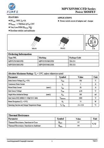
MPVX5N50CCFD Series Power MOSFET MPSW60M041 FEATURES APPLICATIONS BVDSS 500V, ID=5A Power switch circuit of adaptor and charger RDS(on) 1.7 (Max) @VGS=10V Very Low FOM (RDS(on) *Qg) Excellent stability and uniformity D G TO-252 TO-251 S Ordering Information Type NO. Marking Package Code MPVU5N50CCFD MPVU5N50CCFD TO-251 MPVD5N50CCFD MPVD5N50CCFD TO-252 Abso
0.34. Size:265K inchange semiconductor
aod5n50.pdf
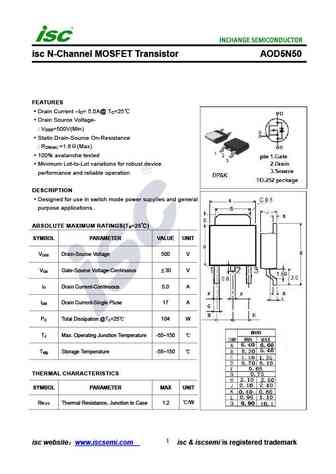
isc N-Channel MOSFET Transistor AOD5N50 FEATURES Drain Current I = 5.0A@ T =25 D C Drain Source Voltage- V =500V(Min) DSS Static Drain-Source On-Resistance R =1.6 (Max) DS(on) 100% avalanche tested Minimum Lot-to-Lot variations for robust device performance and reliable operation DESCRIPTION Designed for use in switch mode power supplies and general purpose
Otros transistores... 110N04, 13N90, 14N65, 18N50D, D2N60, D4N70, D4N80, D50N06, CS150N04A8, DH0159, DH0159B, DH0159D, DH0159E, DH0159F, DH0159I, DH019N04, DH019N04B