5N65C Datasheet. Equivalente. Reemplazo. Hoja de especificaciones. Principales características
Número de Parte: 5N65C 📄📄
Tipo de FET: MOSFET
Polaridad de transistor: N
ESPECIFICACIONES MÁXIMAS
Pdⓘ - Máxima disipación de potencia: 75 W
|Vds|ⓘ - Voltaje máximo drenador-fuente: 650 V
|Vgs|ⓘ - Voltaje máximo fuente-puerta: 30 V
|Id|ⓘ - Corriente continua de drenaje: 5 A
Tjⓘ - Temperatura máxima de unión: 150 °C
CARACTERÍSTICAS ELÉCTRICAS
trⓘ - Tiempo de subida: 16 nS
Cossⓘ - Capacitancia de salida: 53 pF
RDSonⓘ - Resistencia estado encendido drenaje a fuente: 2.7 Ohm
Encapsulados: TO220
📄📄 Copiar
Búsqueda de reemplazo de 5N65C MOSFET
- Selecciónⓘ de transistores por parámetros
5N65C datasheet
..1. Size:1251K cn wxdh
5n65c.pdf 
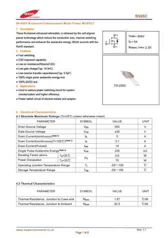
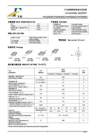
5N65C 5A 650V N-channel Enhancement Mode Power MOSFET 1 Description These N-channel enhanced vdmosfets, is obtained by the self-aligned V DSS = 650V planar technology which reduce the conduction loss, improve switching I = 5A D performance and enhance the avalanche energy. Which accords with the RoHS standard. R DS(on) TYP) = 2.3 2 Features Fast switching ESD improve
0.1. Size:277K infineon
spa15n65c3.pdf
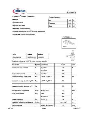
SPA15N65C3 CoolMOSTM Power Transistor Product Summary Features V 650 V DS Low gate charge R 0.28 DS(on),max Extreme dv/dt rated Q 63 nC g,typ High peak current capability Qualified according to JEDEC1) for target applications Pb-free lead plating; RoHS compliant PG-TO220-3-31 Type Package Marking SPA15N65C3 PG-TO220-3-31 15N65C3 Maximum ratings, at T =
0.2. Size:558K infineon
spi15n65c3.pdf
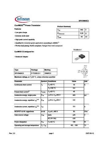
SPI15N65C3 C IMOSTM $;B1= '=- >5>?;= $=;0@/? &@99-=D Features 650 V DS R 'AH 93E7 5 3C97 0.28 W DS(on) max R IEC7?7 6G 6E C3E76 6 nC g typ R #;9 B73= 5FCC7@E 53B34;>;EJ R , F3>;8;76 for industrial grade applications 355AC6;@9 EA % R +4 8C77 >736 B>3E;@9 - A#. 5A?B>;3@E; Halogen free mold compound TO 262 1 ;;8!#& 01>53 10 2;= R ) AE74AA= 63BE7C Type Package Mar
0.3. Size:253K infineon
spp15n65c3.pdf
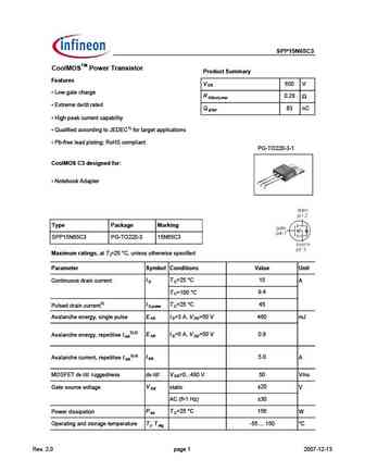
SPP15N65C3 CoolMOSTM Power Transistor Product Summary Features V 650 V DS Low gate charge R 0.28 DS(on),max Extreme dv/dt rated Q 63 nC g,typ High peak current capability Qualified according to JEDEC1) for target applications Pb-free lead plating; RoHS compliant PG-TO220-3-1 CoolMOS C3 designed for Notebook Adapter Type Package Marking SPP15N65C3
0.4. Size:222K ixys
ixyp15n65c3d1.pdf

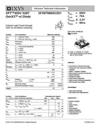
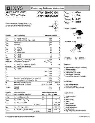
Preliminary Technical Information XPTTM 650V IGBT VCES = 650V IXYA15N65C3D1 GenX3TM w/Diode IC110 = 15A IXYP15N65C3D1 VCE(sat) 2.5V tfi(typ) = 28ns Extreme Light Punch Through IGBT for 20-60kHz Switching TO-263 AA (IXYA) G Symbol Test Conditions Maximum Ratings E C (Tab) VCES TJ = 25 C to 175 C 650 V VCGR
0.5. Size:239K ixys
ixyh75n65c3h1.pdf

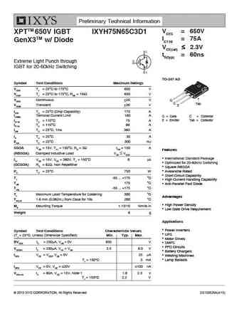
Preliminary Technical Information VCES = 650V XPTTM 650V IGBT IXYH75N65C3H1 IC110 = 75A GenX3TM w/ Sonic VCE(sat) 2.3V Diode tfi(typ) = 50ns Extreme Light Punch through IGBT for 20-60kHz Switching TO-247 AD Symbol Test Conditions Maximum Ratings VCES TJ = 25 C to 175 C 650 V VCGR TJ = 25 C to 175 C, RGE =
0.6. Size:230K ixys
ixyn75n65c3d1.pdf
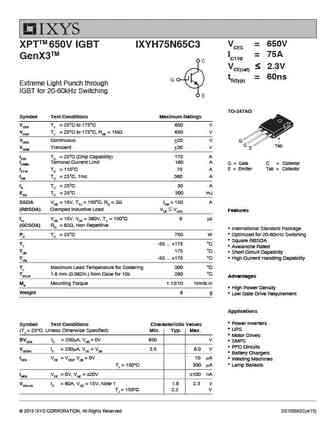
Advance Technical Information VCES = 650V XPTTM 650V IGBT IXYN75N65C3D1 IC110 = 75A GenX3TM w/ Diode VCE(sat) 2.3V tfi(typ) = 60ns Extreme Light Punch through IGBT for 20-60kHz Switching E SOT-227B, miniBLOC E153432 Symbol Test Conditions Maximum Ratings E VCES TJ = 25 C to 175 C 650 V G VCGR TJ = 25
0.7. Size:190K ixys
ixyp15n65c3.pdf
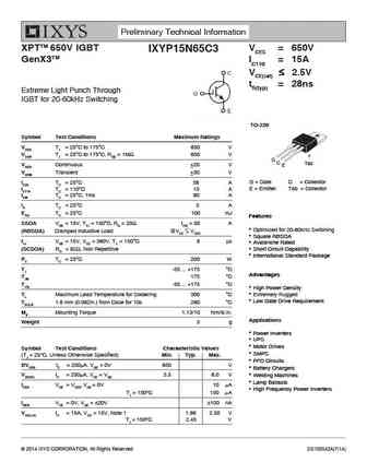
Preliminary Technical Information XPTTM 650V IGBT VCES = 650V IXYP15N65C3 GenX3TM IC110 = 15A VCE(sat) 2.5V tfi(typ) = 28ns Extreme Light Punch Through IGBT for 20-60kHz Switching TO-220 Symbol Test Conditions Maximum Ratings VCES TJ = 25 C to 175 C 650 V VCGR TJ = 25 C to 175 C, RGE = 1M 650 V G C Tab
0.8. Size:195K ixys
ixyp15n65c3d1m.pdf
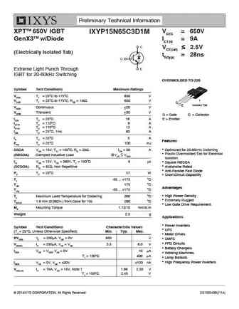
Preliminary Technical Information XPTTM 650V IGBT VCES = 650V IXYP15N65C3D1M GenX3TM w/Diode IC110 = 9A VCE(sat) 2.5V (Electrically Isolated Tab) tfi(typ) = 28ns Extreme Light Punch Through IGBT for 20-60kHz Switching OVERMOLDED TO-220 Symbol Test Conditions Maximum Ratings VCES TJ = 25 C to 175 C 650 V VCGR
0.9. Size:222K ixys
ixya15n65c3d1.pdf
Preliminary Technical Information XPTTM 650V IGBT VCES = 650V IXYA15N65C3D1 GenX3TM w/Diode IC110 = 15A IXYP15N65C3D1 VCE(sat) 2.5V tfi(typ) = 28ns Extreme Light Punch Through IGBT for 20-60kHz Switching TO-263 AA (IXYA) G Symbol Test Conditions Maximum Ratings E C (Tab) VCES TJ = 25 C to 175 C 650 V VCGR
0.10. Size:245K ixys
ixyh75n65c3d1.pdf
Preliminary Technical Information VCES = 650V XPTTM 650V IGBT IXYH75N65C3D1 IC110 = 75A GenX3TM w/ Diode VCE(sat) 2.3V tfi(typ) = 60ns Extreme Light Punch through IGBT for 20-60kHz Switching TO-247 AD Symbol Test Conditions Maximum Ratings VCES TJ = 25 C to 175 C 650 V VCGR TJ = 25 C to 175 C, RGE = 1M 6
0.11. Size:233K ixys
ixyh75n65c3.pdf
VCES = 650V XPTTM 650V IGBT IXYH75N65C3 IC110 = 75A GenX3TM VCE(sat) 2.3V tfi(typ) = 60ns Extreme Light Punch through IGBT for 20-60kHz Switching TO-247AD Symbol Test Conditions Maximum Ratings VCES TJ = 25 C to 175 C 650 V VCGR TJ = 25 C to 175 C, RGE = 1M 650 V VGES Continuous 20 V G C Tab VGEM
0.12. Size:474K sisemi
sif5n65c.pdf
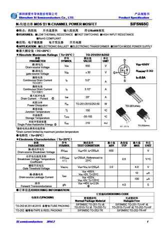
Shenzhen SI Semiconductors Co., LTD. Product Specification Shenzhen SI Semiconductors Co., LTD. Product Specification Shenzhen SI Semiconductors Co., LTD. Product Specification Shenzhen SI Semiconductors Co., LTD. Product Specification N- MOS / N-CHANNEL POWER MOSFET SIF5N65C N- MOS / N-CHANNEL POWER MOSFET SIF5N65C N- MOS / N-CHANN
0.13. Size:1723K jilin sino
jcs15n65fei jcs15n65bei jcs15n65sei jcs15n65cei.pdf
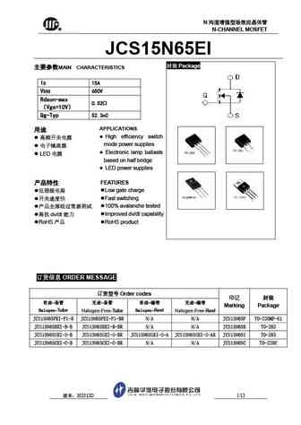
N R N-CHANNEL MOSFET JCS15N65EI Package MAIN CHARACTERISTICS ID 15A VDSS 650V Rdson-max 0.52 Vgs=10V Qg-Typ 52.3nC APPLICATIONS High efficiency switch mode power supplies Electronic lamp ballasts LED based on half bridge
0.14. Size:1312K cn wxdh
f5n65c.pdf
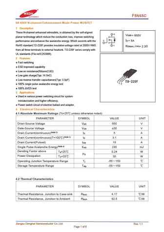
F5N65C 5A 650V N-channel Enhancement Mode Power MOSFET 1 Description These N-channel enhanced vdmosfets, is obtained by the self-aligned V DSS = 650V planar technology which reduce the conduction loss, improve switching I = 5A D performance and enhance the avalanche energy. Which accords with the RoHS standard.TO-220F provides insulation voltage rated at 2000V RMS R DS(on) TYP) =
0.16. Size:829K jiaensemi
jfpc5n65c jffc5n65c.pdf
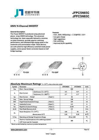
JFPC5N65C JFFC5N65C 650V N-Channel MOSFET General Description Features This Power MOSFET is produced using advanced - 4.5A , 650V, RDS(on)typ. = 2.3 @VGS = 10 V planar stripe DMOS technology. This advanced - Low gate charge technology has been especially tailored to minimize - High ruggedness on-state resistance, provide superior switching - Fast switching performance
0.17. Size:359K maple semi
slp5n65c slf5n65c.pdf
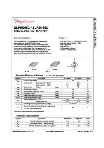
SLP5N65C / SLF5N65C 650V N-Channel MOSFET General Description Features This Power MOSFET is produced using Maple semi s - 4.5A, 650V, RDS(on)typ. = 2.6 @VGS = 10 V advanced planar stripe DMOS technology. - Low gate charge ( typical 16nC) This advanced technology has been especially tailored - High ruggedness to minimize on-state resistance, provide superior switching - Fast switching
0.18. Size:669K way-on
wml15n65c4 wmk15n65c4 wmm15n65c4 wmn15n65c4 wmp15n65c4 wmo15n65c4.pdf
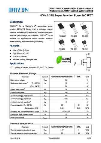
WML1 MM15N65C 15N65C4, WMK15N65C4, WM C4 WMN15N65C4, WMP15N65C4, WM C4 MO15N65C 650V n Power MOSFET V 0.26 Super Junction Descrip ption WMOSTM C4 is Wa 4th generation super ayon s n junction MOSFET fa that is utilizing charge M amily S balance te or extremely esistance echnology fo y low on-re D S D G G G S D G and low ga charge performanc WMOSTM C4
0.19. Size:655K way-on
wml15n65c2 wmk15n65c2 wmm15n65c2 wmn15n65c2 wmp15n65c2 wmo15n65c2.pdf
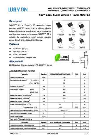
WML1 MM15N65C 15N65C2, WMK15N65C2, WM C2 WMN15N65C2, WMP15N65C2, WM C2 MO15N65C 650V n Power MOSFET V 0.32 Super Junction Descrip ption WMOSTM C2 is Wa 2nd generation super ayon s n junction MOSFET fa that is utilizing charge M amily S balance te or extremely esistance echnology fo y low on-re D S D G G G S D G and low ga charge performanc WMOSTM C2
0.20. Size:630K cn yangzhou yangjie elec
dgw75n65ctl1.pdf
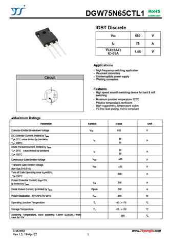
RoHS DGW75N65CTL1 COMPLIANT IGBT Discrete V 650 V CE I 75 A C V CE(SAT) 1.65 V I = A C 75 Applications High frequency switching application Resonant converters Uninterruptible power supply Circuit Welding converters Features High speed smooth switching device for hard & soft switching Maximum junction temperature 175 Pos
0.21. Size:453K cn yangzhou yangjie elec
dgw15n65ctl.pdf
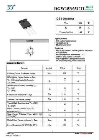
DGW15N65CTL RoHS COMPLIANT IGBT Descrete V 650 V CE I 15 A C V I = A 1.65 V CE(SAT) C 15 Applications Circuit Soft switchingapplications Airconditioning Motor driveinverter Features High speed smooth switching device for hard & soft switching Maximum junction temperature 175 Positive temperature coefficient High ruggedness, temp
0.22. Size:443K cn yangzhou yangjie elec
dgp15n65ctl.pdf
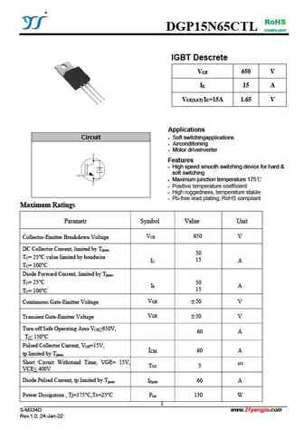
RoHS DGP15N65CTL COMPLIANT IGBT Descrete V 650 V CE I 15 A C V I = A 1.65 V CE(SAT) C 15 Applications Circuit Soft switchingapplications Airconditioning Motor driveinverter Features High speed smooth switching device for hard & soft switching Maximum junction temperature 175 Positive temperature coefficient High ruggedness, te
0.23. Size:200K inchange semiconductor
spa15n65c3.pdf
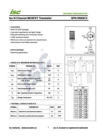
INCHANGE Semiconductor Isc N-Channel MOSFET Transistor SPA15N65C3 FEATURES With TO-220F package Low input capacitance and gate charge Reduced switching and conduction losses 100% avalanche tested Minimum Lot-to-Lot variations for robust device performance and reliable operation APPLICATIONS Switching applications ABSOLUTE MAXIMUM RATINGS(T =25 ) a SYMBOL PARAMET
Otros transistores... DH0159F, DH0159I, DH019N04, DH019N04B, DH019N04D, DH019N04E, 20N65D, 23N50D, K4145, 60N10B, 60N10D, 60N10E, 60N10F, 60N10I, AOB413, B110N04, HYG035N10NS2P