B110N04 MOSFET Equivalente. Reemplazo. Hoja de especificaciones. Principales características
Número de Parte: B110N04
Tipo de FET: MOSFET
Polaridad de transistor: N
ESPECIFICACIONES MÁXIMAS
Pdⓘ - Máxima
disipación de potencia: 120 W
|Vds|ⓘ - Voltaje máximo drenador-fuente: 40 V
|Vgs|ⓘ - Voltaje máximo fuente-puerta: 25 V
|Id|ⓘ - Corriente continua
de drenaje: 160 A
Tjⓘ - Temperatura máxima de unión: 175 °C
CARACTERÍSTICAS ELÉCTRICAS
trⓘ - Tiempo
de subida: 88 nS
Cossⓘ - Capacitancia de salida: 590 pF
RDSonⓘ - Resistencia estado encendido drenaje a fuente: 0.0045 Ohm
Encapsulados: TO251
Búsqueda de reemplazo de B110N04 MOSFET
- Selecciónⓘ de transistores por parámetros
B110N04 datasheet
..1. Size:1381K cn wxdh
110n04 f110n04 i110n04 e110n04 b110n04 d110n04.pdf 
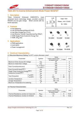
110N04/F110N04/I110N04/ E110N04/B110N04/D110N04 160A 40V N-channel Enhancement Mode Power MOSFET 1 Description These N-channel Enhanced VDMOSFETs Used V = 40V DSS advanced trench technology design, provided excellent RDSON and low gate charge. Which accords with the R = 3.5m DS(on) TYP) RoHS standard. I = 160A D 2 Features Fast Switching Low ON Resistance(Rdson
8.1. Size:334K infineon
ipb110n06lg.pdf
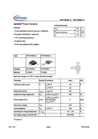
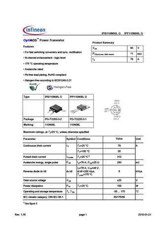
IPB110N06L G IPP110N06L G OptiMOS Power-Transistor Product Summary Features V 60 V DS For fast switching converters and sync. rectification R 11 m DS(on),max SMD version N-channel enhancement - logic level I 78 A D 175 C operating temperature Avalanche rated Pb-free lead plating, RoHS compliant Type IPB110N06L G IPP110N06L G Type Package Marking IPB1
9.1. Size:89K philips
php110nq08t phb110nq08t.pdf
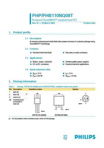
PHP/PHB110NQ08T N-channel TrenchMOS standard level FET Rev. 01 29 March 2004 Product data 1. Product profile 1.1 Description N-channel enhancement mode field-effect power transistor in a plastic package using TrenchMOS technology. 1.2 Features Standard level threshold Very low on-state resistance. 1.3 Applications Motors, lamps, solenoids Uninterruptible power supplies D
9.2. Size:209K philips
phb110nq06lt.pdf
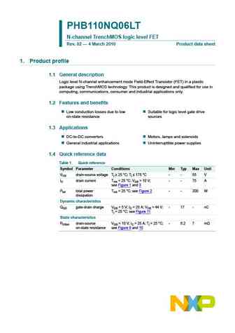
PHB110NQ06LT N-channel TrenchMOS logic level FET Rev. 02 4 March 2010 Product data sheet 1. Product profile 1.1 General description Logic level N-channel enhancement mode Field-Effect Transistor (FET) in a plastic package using TrenchMOS technology. This product is designed and qualified for use in computing, communications, consumer and industrial applications only. 1.2 Features
9.3. Size:89K philips
phb110nq08lt php110nq08lt.pdf

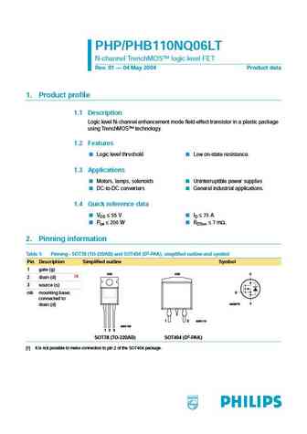
PHP/PHB110NQ08LT N-channel TrenchMOS logic level FET Rev. 01 29 March 2004 Product data 1. Product profile 1.1 Description Logic level N-channel enhancement mode field-effect transistor in a plastic package using TrenchMOS technology. 1.2 Features Logic level threshold Very low on-state resistance. 1.3 Applications Motors, lamps, solenoids Uninterruptible power supplies
9.4. Size:94K philips
php110nq06lt phb110nq06lt.pdf
PHP/PHB110NQ06LT N-channel TrenchMOS logic level FET Rev. 01 04 May 2004 Product data 1. Product profile 1.1 Description Logic level N-channel enhancement mode field-effect transistor in a plastic package using TrenchMOS technology. 1.2 Features Logic level threshold Low on-state resistance. 1.3 Applications Motors, lamps, solenoids Uninterruptible power supplies DC-to-D
9.5. Size:695K fairchild semi
fcb110n65f.pdf
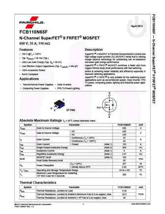
April 2015 FCB110N65F N-Channel SuperFET II FRFET MOSFET 650 V, 35 A, 110 m Features Description 700 V @TJ = 150 C SuperFET II MOSFET is Fairchild Semiconductor s brand-new high voltage super-junction (SJ) MOSFET family that is utilizing Typ. RDS(on) = 96 m (Typ.) charge balance technology for outstanding low on-resistance Ultra Low Gate Charge (Typ. Qg = 98 nC
9.7. Size:674K nxp
phb110nq08t.pdf
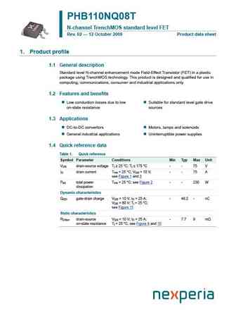
PHB110NQ08T N-channel TrenchMOS standard level FET Rev. 02 12 October 2009 Product data sheet 1. Product profile 1.1 General description Standard level N-channel enhancement mode Field-Effect Transistor (FET) in a plastic package using TrenchMOS technology. This product is designed and qualified for use in computing, communications, consumer and industrial applications only. 1.2 F
9.8. Size:991K infineon
ipb110n20n3lf.pdf
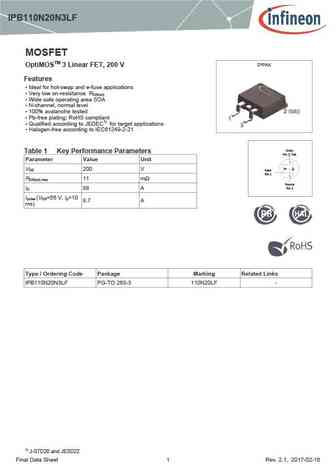
IPB110N20N3LF MOSFET D PAK OptiMOSTM 3 Linear FET, 200 V Features Ideal for hot-swap and e-fuse applications Very low on-resistance R DS(on) Wide safe operating area SOA N-channel, normal level 100% avalanche tested Pb-free plating; RoHS compliant Qualified according to JEDEC1) for target applications Halogen-free according to IEC61249-2-21 Drain
9.9. Size:803K onsemi
fcb110n65f.pdf

Is Now Part of To learn more about ON Semiconductor, please visit our website at www.onsemi.com Please note As part of the Fairchild Semiconductor integration, some of the Fairchild orderable part numbers will need to change in order to meet ON Semiconductor s system requirements. Since the ON Semiconductor product management systems do not have the ability to manage part nomenclatur
9.10. Size:466K onsemi
ntb110n65s3hf.pdf
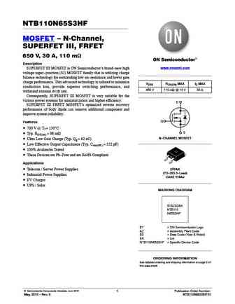
NTB110N65S3HF MOSFET N Channel, SUPERFET III, FRFET 650 V, 30 A, 110 mW Description www.onsemi.com SUPERFET III MOSFET is ON Semiconductor s brand-new high voltage super-junction (SJ) MOSFET family that is utilizing charge balance technology for outstanding low on-resistance and lower gate charge performance. This advanced technology is tailored to minimize VDSS RDS(ON) MAX ID
9.11. Size:235K onsemi
nvb110n65s3f.pdf
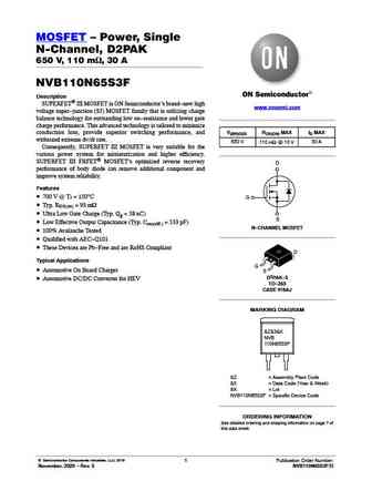
MOSFET Power, Single N-Channel, D2PAK 650 V, 110 mW, 30 A NVB110N65S3F Description SUPERFET III MOSFET is ON Semiconductor s brand-new high www.onsemi.com voltage super-junction (SJ) MOSFET family that is utilizing charge balance technology for outstanding low on-resistance and lower gate charge performance. This advanced technology is tailored to minimize V(BR)DSS RDS(ON) MAX
9.12. Size:777K onsemi
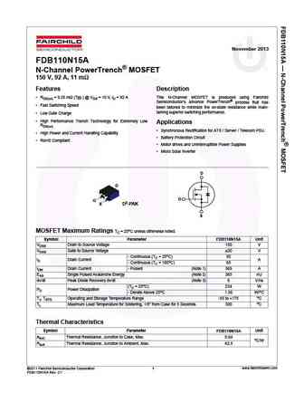
fdb110n15a.pdf

Is Now Part of To learn more about ON Semiconductor, please visit our website at www.onsemi.com Please note As part of the Fairchild Semiconductor integration, some of the Fairchild orderable part numbers will need to change in order to meet ON Semiconductor s system requirements. Since the ON Semiconductor product management systems do not have the ability to manage part nomenclatur
9.13. Size:830K cn hunteck
hgb110n10sl hgp110n10sl.pdf
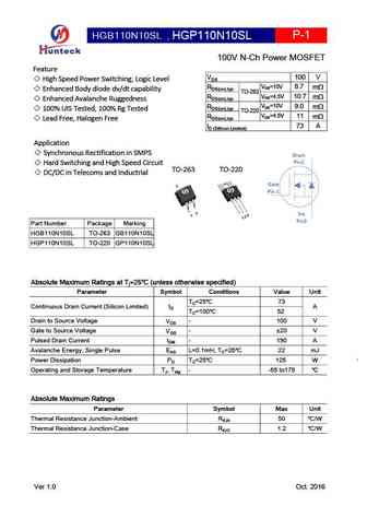
HGB110N10SL , HGP110N10SL P-1 100V N-Ch Power MOSFET Feature 100 V VDS High Speed Power Switching, Logic Level 8.7 RDS(on),typ TO-263 VGS=10V m Enhanced Body diode dv/dt capability VGS=4.5V 10.7 RDS(on),typ m Enhanced Avalanche Ruggedness 9.0 RDS(on),typ TO-220 VGS=10V m 100% UIS Tested, 100% Rg Tested VGS=4.5V 11 RDS(on),typ m Lead Free, Halog
9.14. Size:883K cn hunteck
hgb110n20s hgk110n20s hgp110n20s.pdf
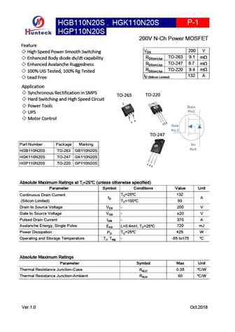
, HGB110N20S HGK110N20S P-1 HGP110N20S 200V N-Ch Power MOSFET Feature 200 V VDS High Speed Power Smooth Switching TO-263 9.1 RDS(on),typ m Enhanced Body diode dv/dt capability TO-247 8.7 RDS(on),typ m Enhanced Avalanche Ruggedness TO-220 9.4 RDS(on),typ m 100% UIS Tested, 100% Rg Tested 132 A ID (Sillicon Limited) Lead Free Application Synch
9.15. Size:254K inchange semiconductor
fcb110n65f.pdf
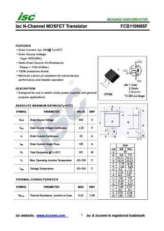
isc N-Channel MOSFET Transistor FCB110N65F FEATURES Drain Current I = 35A@ T =25 D C Drain Source Voltage- V = 650V(Min) DSS Static Drain-Source On-Resistance R = 110m (Max) DS(on) 100% avalanche tested Minimum Lot-to-Lot variations for robust device performance and reliable operation DESCRIPTION Designed for use in switch mode power supplies and general pu
9.16. Size:258K inchange semiconductor
ipb110n20n3lf.pdf
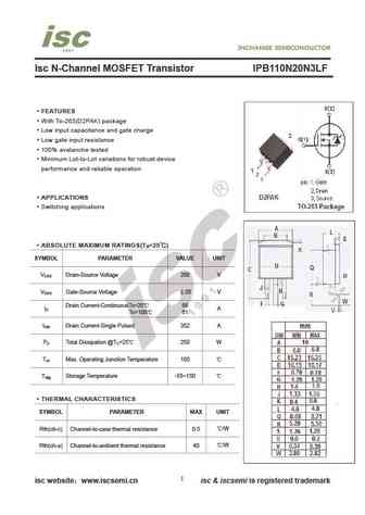
Isc N-Channel MOSFET Transistor IPB110N20N3LF FEATURES With To-263(D2PAK) package Low input capacitance and gate charge Low gate input resistance 100% avalanche tested Minimum Lot-to-Lot variations for robust device performance and reliable operation APPLICATIONS Switching applications ABSOLUTE MAXIMUM RATINGS(T =25 ) a SYMBOL PARAMETER VALUE UNIT V Drain-Source
9.17. Size:260K inchange semiconductor
fdb110n15a.pdf
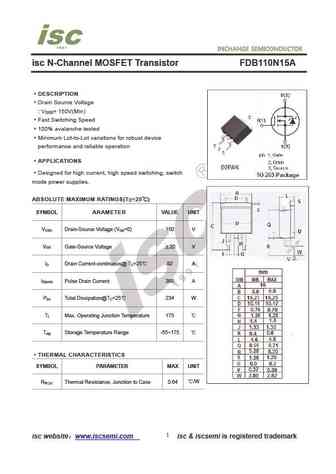
isc N-Channel MOSFET Transistor FDB110N15A DESCRIPTION Drain Source Voltage V = 150V(Min) DSS Fast Switching Speed 100% avalanche tested Minimum Lot-to-Lot variations for robust device performance and reliable operation APPLICATIONS . Designed for high current, high speed switching, switch mode power supplies. ABSOLUTE MAXIMUM RATINGS(T =25 ) C SYMBOL ARAMETER VA
Otros transistores... 23N50D
, 5N65C
, 60N10B
, 60N10D
, 60N10E
, 60N10F
, 60N10I
, AOB413
, AO3400A
, HYG035N10NS2P
, HYG035N10NS2B
, JMTE070N07A
, DH012N03D
, DH012N03E
, DH012N03F
, DH012N03I
, DH012N03P
.
History: 60N10D
| WMP11N65SR
| WML125N12LG2
| WML12N105C2