D7N60 MOSFET Equivalente. Reemplazo. Hoja de especificaciones. Principales características
Número de Parte: D7N60
Tipo de FET: MOSFET
Polaridad de transistor: N
ESPECIFICACIONES MÁXIMAS
Pdⓘ - Máxima
disipación de potencia: 100 W
|Vds|ⓘ - Voltaje máximo drenador-fuente: 600 V
|Vgs|ⓘ - Voltaje máximo fuente-puerta: 30 V
|Id|ⓘ - Corriente continua
de drenaje: 7 A
Tjⓘ - Temperatura máxima de unión: 150 °C
CARACTERÍSTICAS ELÉCTRICAS
trⓘ - Tiempo
de subida: 22 nS
Cossⓘ - Capacitancia de salida: 96 pF
RDSonⓘ - Resistencia estado encendido drenaje a fuente: 1.25 Ohm
Encapsulados: TO252
Búsqueda de reemplazo de D7N60 MOSFET
- Selecciónⓘ de transistores por parámetros
D7N60 datasheet
..1. Size:1261K cn wxdh
d7n60.pdf 
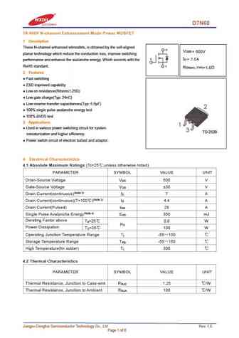
D7N60 7A 600V N-channel Enhancement Mode Power MOSFET 1 Description These N-channel enhanced vdmosfets, is obtained by the self-aligned V DSS = 600V planar technology which reduce the conduction loss, improve switching I = 7.0A D performance and enhance the avalanche energy. Which accords with the RoHS standard. R DS(on) TYP) =1.0 2 Features Fast switching ESD improv
0.1. Size:166K 1
hgtd7n60c3s hgtp7n60c3.pdf

HGTD7N60C3S, HGTP7N60C3 Data Sheet December 2001 14A, 600V, UFS Series N-Channel IGBTs Features The HGTD7N60C3S and HGTP7N60C3 are MOS gated 14A, 600V at TC = 25oC high voltage switching devices combining the best features 600V Switching SOA Capability of MOSFETs and bipolar transistors. These devices have the Typical Fall Time. . . . . . . . . . . . . . . . 140ns at TJ =
0.5. Size:1199K st
std7n60m2 stp7n60m2 stu7n60m2.pdf
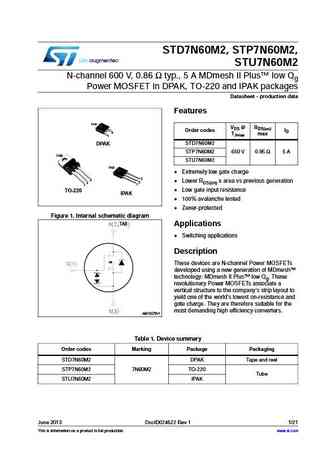
STD7N60M2, STP7N60M2, STU7N60M2 N-channel 600 V, 0.86 typ., 5 A MDmesh II Plus low Qg Power MOSFET in DPAK, TO-220 and IPAK packages Datasheet - production data Features TAB VDS @ RDS(on) Order codes ID 3 TJmax max 1 STD7N60M2 DPAK STP7N60M2 650 V 0.95 5 A TAB STU7N60M2 TAB Extremely low gate charge 3 3 2 Lower RDS(on) x area vs previous generation 2 1
0.6. Size:161K fairchild semi
hgtd7n60c3s hgtp7n60c3.pdf
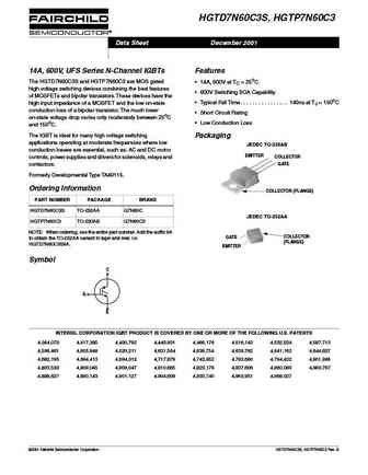
HGTD7N60C3S, HGTP7N60C3 Data Sheet December 2001 14A, 600V, UFS Series N-Channel IGBTs Features The HGTD7N60C3S and HGTP7N60C3 are MOS gated 14A, 600V at TC = 25oC high voltage switching devices combining the best features 600V Switching SOA Capability of MOSFETs and bipolar transistors. These devices have the Typical Fall Time. . . . . . . . . . . . . . . . 140ns at TJ =
0.7. Size:663K fairchild semi
fdd7n60nz fdd7n60nztm fdu7n60nztu.pdf
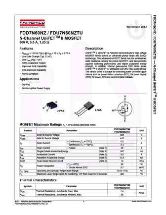
November 2013 FDD7N60NZ / FDU7N60NZTU N-Channel UniFETTM II MOSFET 600 V, 5.5 A, 1.25 Features Description RDS(on) = 1.05 (Typ.) @ VGS = 10 V, ID = 2.75 A UniFETTM II MOSFET is Fairchild Semiconductor s high voltage MOSFET family based on advanced planar stripe and DMOS Low Gate Charge (Typ. 13 nC) technology. This advanced MOSFET family has the smallest on- Low Crs
0.8. Size:1005K fairchild semi
fcd7n60 fcu7n60.pdf
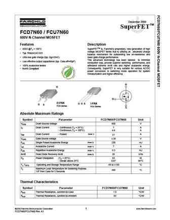
December 2008 TM SuperFET FCD7N60 / FCU7N60 600V N-Channel MOSFET Features Description 650V @TJ = 150 C SuperFETTM is, Fairchild s proprietary, new generation of high voltage MOSFET family that is utilizing an advanced charge Typ. Rds(on)=0.53 balance mechanism for outstanding low on-resistance and Ultra low gate charge (typ. Qg=23nC) lower gate charge performan
0.9. Size:188K vishay
sihd7n60e.pdf
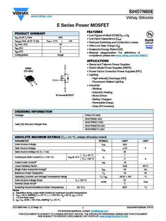
SiHD7N60E www.vishay.com Vishay Siliconix E Series Power MOSFET FEATURES PRODUCT SUMMARY Low Figure-of-Merit (FOM) Ron x Qg VDS (V) at TJ max. 650 Low Input Capacitance (Ciss) RDS(on) max. at 25 C ( ) VGS = 10 V 0.6 Reduced Switching and Conduction Losses Qg max. (nC) 40 Ultra Low Gate Charge (Qg) Qgs (nC) 5 Avalanche Energy Rated (UIS) Qgd (nC) 9 Mate
0.10. Size:282K onsemi
hgtd7n60c3s hgtp7n60c3.pdf

Is Now Part of To learn more about ON Semiconductor, please visit our website at www.onsemi.com Please note As part of the Fairchild Semiconductor integration, some of the Fairchild orderable part numbers will need to change in order to meet ON Semiconductor s system requirements. Since the ON Semiconductor product management systems do not have the ability to manage part nomenclatur
0.11. Size:543K onsemi
fcd7n60.pdf

Is Now Part of To learn more about ON Semiconductor, please visit our website at www.onsemi.com Please note As part of the Fairchild Semiconductor integration, some of the Fairchild orderable part numbers will need to change in order to meet ON Semiconductor s system requirements. Since the ON Semiconductor product management systems do not have the ability to manage part nomenclatur
0.12. Size:222K harris semi
hgtd7n60.pdf
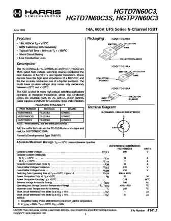
HGTD7N60C3, S E M I C O N D U C T O R HGTD7N60C3S, HGTP7N60C3 14A, 600V, UFS Series N-Channel IGBT June 1996 Features Packaging JEDEC TO-220AB 14A, 600V at TC = +25oC COLLECTOR EMITTER 600V Switching SOA Capability GATE Typical Fall Time - 140ns at TJ = +150oC Short Circuit Rating Low Conduction Loss COLLECTOR (FLANGE) Description JEDEC TO-251AA The HGTD7N60C
0.13. Size:387K aosemi
aod7n60 aoi7n60.pdf

AOD7N60/AOI7N60 600V,7A N-Channel MOSFET General Description Product Summary The AOD7N60 & AOI7N60 have been fabricated using an advanced high voltage MOSFET process that is designed VDS 700V@150 to deliver high levels of performance and robustness in ID (at VGS=10V) 7A popular AC-DC applications. RDS(ON) (at VGS=10V)
0.14. Size:387K aosemi
aod7n60.pdf
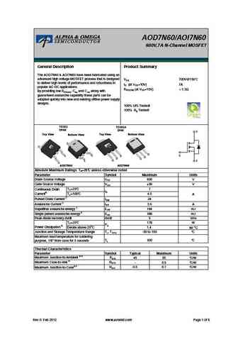
AOD7N60/AOI7N60 600V,7A N-Channel MOSFET General Description Product Summary The AOD7N60 & AOI7N60 have been fabricated using an advanced high voltage MOSFET process that is designed VDS 700V@150 to deliver high levels of performance and robustness in ID (at VGS=10V) 7A popular AC-DC applications. RDS(ON) (at VGS=10V)
0.15. Size:1016K blue-rocket-elect
brd7n60.pdf
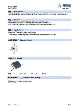
BRD7N60 Rev.E Feb.-2017 DATA SHEET / Descriptions TO-252 N MOS N-CHANNEL MOSFET in a TO-252 Plastic Package. / Features 600V MOSFET, , , 600V Enhanced Power MOSFET, Low gate charge, low crss, fast switching. / Applications
0.16. Size:999K samwin
sw7n60d swf7n60d swp7n60d swi7n60d swd7n60d.pdf
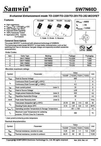
SW7N60D N-channel Enhancement mode TO-220F/TO-220/TO-251/TO-252 MOSFET Features TO-220F TO-220 TO-251 TO-252 BVDSS 600V High ruggedness ID 7A RDS(ON) (Typ 1.05 )@VGS=10V RDS(ON) 1.05 Gate Charge (Typ 30nC) Improved dv/dt Capability 2 100% Avalanche Tested 1 1 1 1 2 2 2 2 Application UPS Inverter 3 3 3 3 TV
0.17. Size:1026K samwin
swf7n60d swp7n60d swi7n60d swd7n60d.pdf
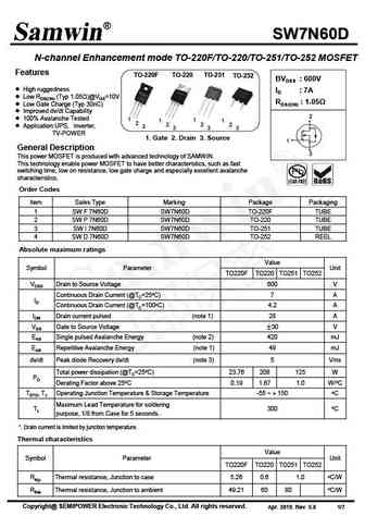
SW7N60D N-channel Enhancement mode TO-220F/TO-220/TO-251/TO-252 MOSFET Features TO-220F TO-220 TO-251 TO-252 BVDSS 600V High ruggedness ID 7A Low RDS(ON) (Typ 1.05 )@VGS=10V RDS(ON) 1.05 Low Gate Charge (Typ 30nC) Improved dv/dt Capability 2 100% Avalanche Tested 1 1 1 1 2 2 2 2 Application UPS Inverter 3 3 3
0.18. Size:608K samwin
swd7n60k2f.pdf
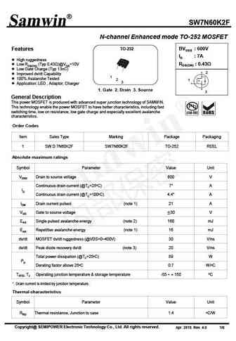
SW7N60K2F N-channel Enhanced mode TO-252 MOSFET TO-252 BVDSS 600V Features ID 7A High ruggedness RDS(ON) 0.43 Low RDS(ON) (Typ 0.43 )@VGS=10V Low Gate Charge (Typ 13nC) 2 Improved dv/dt Capability 1 100% Avalanche Tested 2 1 3 Application LED , Adaptor, Charger 1. Gate 2. Drain 3. Source 3 General Description This pow
0.19. Size:457K trinnotech
tmd7n60z tmu7n60z.pdf
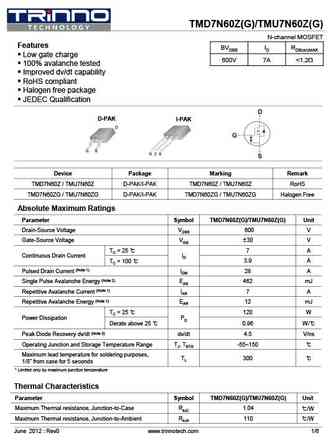
TMD7N60Z(G)/TMU7N60Z(G) N-channel MOSFET Features BVDSS ID RDS(on)MAX Low gate charge 600V 7A
0.21. Size:1036K lonten
lnc7n60d lnd7n60d lng7n60d lnh7n60d.pdf
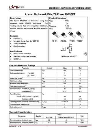
LNC7N60D LND7N60D LNG7N60D LNH7N60D Lonten N-channel 600V, 7A Power MOSFET Description Product Summary The Power MOSFET is fabricated using the VDSS 600V advanced planar VDMOS technology. The ID 7A resulting device has low conduction resistance, RDS(on),max 1.3 superior switching performance and high avalance Qg,typ 20.6nC energy. Features Low RDS(on) Low gate cha
0.22. Size:940K lonten
lnc7n60 lnd7n60.pdf
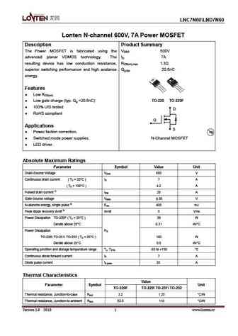
LNC7N60 LND7N60 Lonten N-channel 600V, 7A Power MOSFET Description Product Summary The Power MOSFET is fabricated using the VDSS 600V advanced planar VDMOS technology. The ID 7A resulting device has low conduction resistance, RDS(on),max 1.3 superior switching performance and high avalance Qg,typ 20.6nC energy. Features Low RDS(on) Low gate charge (typ. Qg =20.6nC
0.23. Size:559K cn wuxi unigroup
tma7n60h tmc7n60h tmd7n60h tmu7n60h.pdf
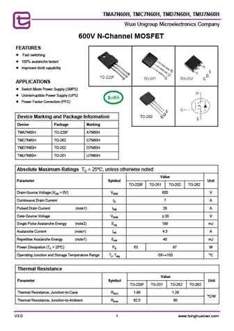
TMA7N60H, TMC7N60H, TMD7N60H, TMU7N60H Wuxi Unigroup Microelectronics Company 600V N-Channel MOSFET FEATURES Fast switching 100% avalanche tested Improved dv/dt capability APPLICATIONS Switch Mode Power Supply (SMPS) Uninterruptible Power Supply (UPS) Power Factor Correction (PFC) Device Marking and Package Information Device Package Marking TM
0.24. Size:265K inchange semiconductor
aod7n60.pdf
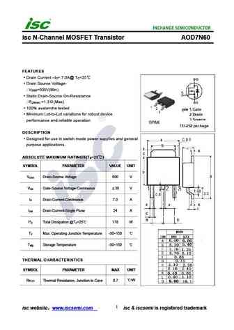
isc N-Channel MOSFET Transistor AOD7N60 FEATURES Drain Current I = 7.0A@ T =25 D C Drain Source Voltage- V =600V(Min) DSS Static Drain-Source On-Resistance R =1.3 (Max) DS(on) 100% avalanche tested Minimum Lot-to-Lot variations for robust device performance and reliable operation DESCRIPTION Designed for use in switch mode power supplies and general purpose
0.25. Size:288K inchange semiconductor
fdd7n60nz.pdf
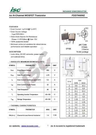
isc N-Channel MOSFET Transistor FDD7N60NZ FEATURES Drain Current I =5.5A@ T =25 D C Drain Source Voltage V =600V(Min) DSS Static Drain-Source On-Resistance R =1.25 (Max) @ V = 10V DS(on) GS 100% avalanche tested Minimum Lot-to-Lot variations for robust device performance and reliable operation DESCRIPTION motor drive, DC-DC converter, power switch and soleno
Otros transistores... DH012N03B
, D12N06
, D18N20
, D25N10
, D5N65-XAD
, D630
, D640
, D740
, 7N65
, D7N70
, D80N06
, D8N50
, D9N65
, 18P10
, 18P10B
, 18P10D
, 18P10E
.