F8N65 MOSFET Equivalente. Reemplazo. Hoja de especificaciones. Principales características
Número de Parte: F8N65
Tipo de FET: MOSFET
Polaridad de transistor: N
ESPECIFICACIONES MÁXIMAS
Pdⓘ - Máxima
disipación de potencia: 35 W
|Vds|ⓘ - Voltaje máximo drenador-fuente: 650 V
|Vgs|ⓘ - Voltaje máximo fuente-puerta: 30 V
|Id|ⓘ - Corriente continua
de drenaje: 8 A
Tjⓘ - Temperatura máxima de unión: 150 °C
CARACTERÍSTICAS ELÉCTRICAS
trⓘ - Tiempo
de subida: 21 nS
Cossⓘ - Capacitancia de salida: 95 pF
RDSonⓘ - Resistencia estado encendido drenaje a fuente: 1.4 Ohm
Encapsulados: TO220F
Búsqueda de reemplazo de F8N65 MOSFET
- Selecciónⓘ de transistores por parámetros
F8N65 datasheet
..1. Size:1383K cn wxdh
f8n65.pdf 
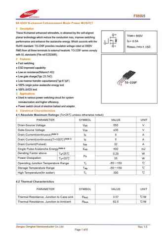
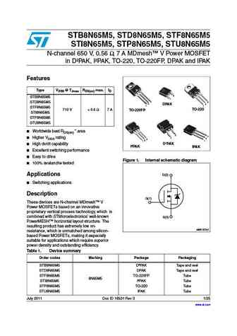
F8N65 8A 650V N-channel Enhancement Mode Power MOSFET 1 Description These N-channel enhanced vdmosfets, is obtained by the self-aligned V DSS = 650V planar technology which reduce the conduction loss, improve switching I = 8.0A D performance and enhance the avalanche energy. Which accords with the RoHS standard. TO-220F provides insulation voltage rated at 2000V R DS(on) TYP) =1.
0.3. Size:506K aosemi
aot8n65 aotf8n65.pdf

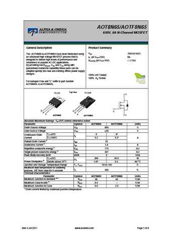
AOT8N65/AOTF8N65 650V, 8A N-Channel MOSFET General Description Product Summary VDS 750V@150 The AOT8N65 & AOTF8N65 have been fabricated using an advanced high voltage MOSFET process that is ID (at VGS=10V) 8A designed to deliver high levels of performance and RDS(ON) (at VGS=10V)
0.4. Size:154K aosemi
aotf8n65.pdf
AOT8N65/AOTF8N65 650V, 8A N-Channel MOSFET General Description Product Summary VDS 750V@150 The AOT8N65 & AOTF8N65 have been fabricated using an advanced high voltage MOSFET process that is ID (at VGS=10V) 8A designed to deliver high levels of performance and RDS(ON) (at VGS=10V)
0.5. Size:434K silikron
ssf8n65.pdf
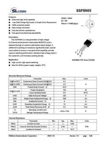
SSF8N65 Features VDSS = 650V Extremely high dv/dt capability ID = 8A Low Gate Charge Qg results in Simple Drive Requirement Rdson = 0.95 (typ.) 100% avalanche tested Gate charge minimized Very low intrinsic capacitances Very good manufacturing repeatability Description The SSF8N65 is a new generation of high voltage N Channel enhancement mod
0.6. Size:979K blue-rocket-elect
brf8n65.pdf
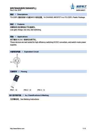
BRF8N65(BRCS8N65FL) Rev.C Feb.-2015 DATA SHEET / Descriptions TO-220FL N MOS N-CHANNEL MOSFET in a TO-220FL Plastic Package. / Features , , Low gate charge, low crss, fast switching. / Applications DC/DC These devices are well suited for hi
0.9. Size:215K winsemi
wff8n65l.pdf
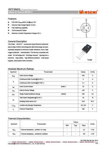
WFF8N65L Product Description Silicon N-Channel MOSFET Silicon N-Channel MOSFET Silicon N-Channel MOSFET Silicon N-Channel MOSFET Features D 8.0A,650V,R (Max1.4 )@V =10V DS(on) GS Ultra-low Gate charge(Typical 14.5nC) Fast Switching Capability G 100%Avalanche Tested Maximum Junction Temperature Range(150 ) S General Description This Power MOSFET is produce
0.10. Size:695K winsemi
wff8n65b.pdf
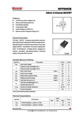
WFF8N65B WFF8N65B WFF8N65B WFF8N65B Silicon N-Channel MOSFET Silicon N-Channel MOSFET Silicon N-Channel MOSFET Silicon N-Channel MOSFET Features 7.5A,650V,R (Max1.3 )@V =10V DS(on) GS Ultra-low Gate charge(Typical 25nC) Fast Switching Capability 100%Avalanche Tested Isolation Voltage (V =4000V AC) ISO Maximum Junction Temperature Range(150 ) General
0.11. Size:970K feihonltd
fhp8n65a fhf8n65a.pdf
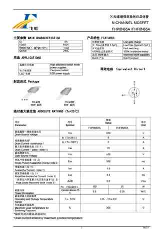
N N-CHANNEL MOSFET FHP8N65A /FHF8N65A MAIN CHARACTERISTICS FEATURES ID 8A Low gate charge VDSS 650V Crss ( 5.5pF) Low Crss (typical 5.5pF ) Rdson-typ @Vgs=10V 1.0 Fast switching Qg-typ 24nC 100% 100% avalanche tested dv/dt Impr
0.13. Size:361K maple semi
slp8n65c slf8n65c.pdf
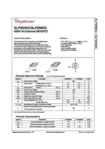
SLP8N65C/SLF8N65C 650V N-Channel MOSFET General Description Features This Power MOSFET is produced using Maple semi s - 7.5A, 650V, RDS(on) typ. = 1.2 @VGS = 10 V advanced planar stripe DMOS technology. - Low gate charge ( typical 29nC) This advanced technology has been especially tailored - High ruggedness to minimize on-state resistance, provide superior switching - Fast switching p
0.14. Size:1171K samwin
swp8n65d swi8n65d swd8n65d swf8n65d swnx8n65d.pdf
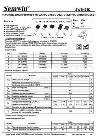
SW8N65D N-channel Enhanced mode TO-220/TO-251/TO-252/TO-220F/TO-251NX MOSFET BVDSS 650V Features TO-220 TO-251 TO-252 TO-220F TO-251NX ID 8A High ruggedness RDS(ON) 1.1 Low RDS(ON) (Typ 1.1 )@VGS=10V Low Gate Charge (Typ 32nC) 2 Improved dv/dt Capability 1 1 1 1 100% Avalanche Tested 1 2 2 2 2 2 3 3 3 3 Application Charg
0.15. Size:1132K samwin
sw8n65db swi8n65db swd8n65db swf8n65db swj8n65db.pdf
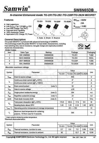
SW8N65DB N-channel Enhanced mode TO-251/TO-252 /TO-220F/TO-262N MOSFET Features BVDSS 650V TO-251 TO-252 TO-220F TO-262N ID 8A High ruggedness Low RDS(ON) (Typ 1.0 )@VGS=10V RDS(ON) 1.0 Low Gate Charge (Typ 34nC) 2 Improved dv/dt Capability 1 100% Avalanche Tested 1 1 1 2 2 2 2 Application LED, Charge, PC Power 3 3 3 3 1
0.16. Size:1066K samwin
swi8n65db swd8n65db swf8n65db swj8n65db.pdf
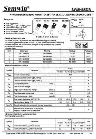
SW8N65DB N-channel Enhanced mode TO-251/TO-252 /TO-220F/TO-262N MOSFET Features BVDSS 650V TO-251 TO-252 TO-220F TO-262N ID 8A High ruggedness Low RDS(ON) (Typ 1.0 )@VGS=10V RDS(ON) 1.0 Low Gate Charge (Typ 34nC) 2 Improved dv/dt Capability 1 100% Avalanche Tested 1 1 1 2 2 2 2 Application LED, Charger, PC Power 3 3 3 3 1 1. Gate 2. Drain
0.17. Size:1169K truesemi
tsp8n65m tsf8n65m.pdf
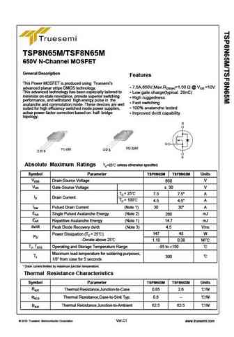
TSP8N65M/TSF8N65M 650V N-Channel MOSFET General Description Features This Power MOSFET is produced using Truesemi s 7.5A,650V,Max.RDS(on)=1.50 @ VGS =10V advanced planar stripe DMOS technology. This advanced technology has been especially tailored to Low gate charge(typical 29nC) minimize on-state resistance, provide superior switching High ruggedness performance, an
0.18. Size:867K huake
smf8n65.pdf
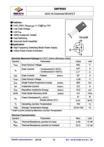
SMF8N65 650V N-Channnel MOSFET Features 8.0A, 650V, R =1.1 @V =10V DS(on)(Typ) GS Low Gate Charge Low C rss 100% Avalanche Tested Fast Switching Improved dv/dt Capability Application High Frequency Switching Mode Power Supply Active Power Factor Correction Absolute Maximum Ratings(Tc=25 C unless otherwise noted) Symbol Parameter Value
0.19. Size:6056K cn puolop
ptf8n65.pdf
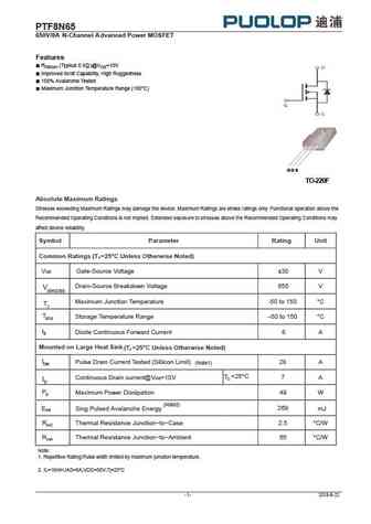
PTF8 N65 65 0V/8 A N-Channel A dv anced Power MOSFET Features RDS(on) (Typical 0.9 )@VGS=10V Improved dv/dt Capability, High Ruggedness 100% Avalanche Tested Maximum Junction Temperature Range (150 C) G D S TO-220F Absolute Maximum Ratings Stresses exceeding Maximum Ratings may damage the device. Maximum Ratings are stress ratings only. Functional operation above t
0.20. Size:1406K cn sps
smirf8n65.pdf
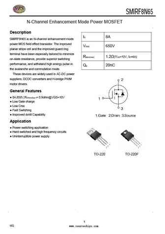
SMIRF8N65 30V /36A Single N Power MOSFET N-Channel Enhancement Mode Power MOSFET Description ID 8A SMIRF8N65 is an N-channel enhancement mode power MOS field effect transistor. The improved VDSS 650V planar stripe cell and the improved guard ring terminal have been especially tailored to minimize Rdson(max) 1.2 (VGS=10V, ID=4A) on-state resistance, provide superior switchi
0.21. Size:715K cn minos
mpf8n65.pdf
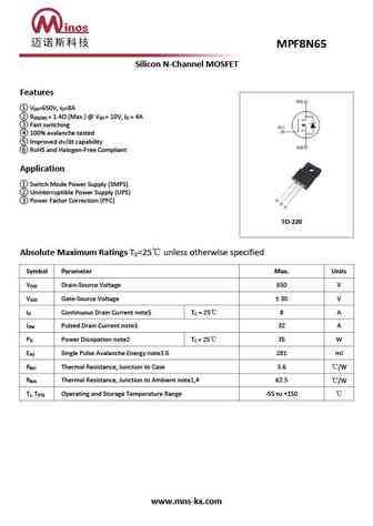
Silicon N-Channel MOSFET Features V =650V, I =8A DS D R = 1.4 (Max.) @ V = 10V, I = 4A DS(ON) GS D Fast switching 100% avalanche tested Improved dv/dt capability RoHS and Halogen-Free Compliant Application Switch Mode Power Supply (SMPS) Uninterruptible Power Supply (UPS) Power Factor Correction (PFC) TO-220 Absolute Maximum Ratings T =25
0.22. Size:201K inchange semiconductor
stf8n65m5.pdf
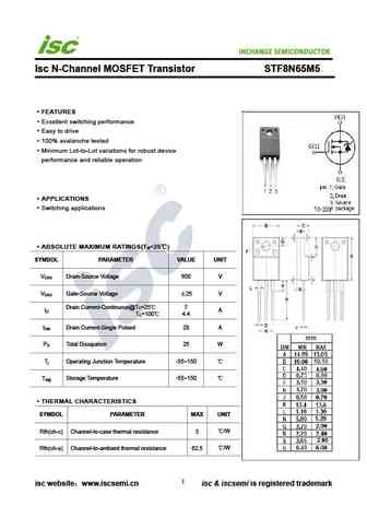
INCHANGE Semiconductor Isc N-Channel MOSFET Transistor STF8N65M5 FEATURES Excellent switching performance Easy to drive 100% avalanche tested Minimum Lot-to-Lot variations for robust device performance and reliable operation APPLICATIONS Switching applications ABSOLUTE MAXIMUM RATINGS(T =25 ) a SYMBOL PARAMETER VALUE UNIT V Drain-Source Voltage 650 V DSS V Gate-
0.23. Size:252K inchange semiconductor
aotf8n65.pdf
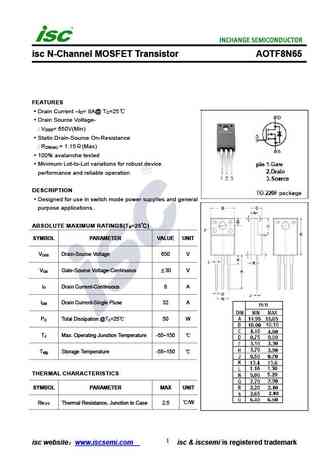
isc N-Channel MOSFET Transistor AOTF8N65 FEATURES Drain Current I = 8A@ T =25 D C Drain Source Voltage- V = 650V(Min) DSS Static Drain-Source On-Resistance R = 1.15 (Max) DS(on) 100% avalanche tested Minimum Lot-to-Lot variations for robust device performance and reliable operation DESCRIPTION Designed for use in switch mode power supplies and general purpo
Otros transistores... F6N90, F740, F7N60, F7N70, F7N80, F80N06, F8N50, F8N60, IRF4905, FD120N10ZR, FN6005, I110N04, I20N50, I25N10, I50N06, I630, I640