AGM10N15R Datasheet. Equivalente. Reemplazo. Hoja de especificaciones. Principales características
Número de Parte: AGM10N15R 📄📄
Tipo de FET: MOSFET
Polaridad de transistor: N
ESPECIFICACIONES MÁXIMAS
Pdⓘ - Máxima disipación de potencia: 39 W
|Vds|ⓘ - Voltaje máximo drenador-fuente: 150 V
|Vgs|ⓘ - Voltaje máximo fuente-puerta: 20 V
|Id|ⓘ - Corriente continua de drenaje: 8.2 A
Tjⓘ - Temperatura máxima de unión: 150 °C
CARACTERÍSTICAS ELÉCTRICAS
trⓘ - Tiempo de subida: 10.2 nS
Cossⓘ - Capacitancia de salida: 23 pF
RDSonⓘ - Resistencia estado encendido drenaje a fuente: 0.3 Ohm
Encapsulados: SOT223
📄📄 Copiar
Búsqueda de reemplazo de AGM10N15R MOSFET
- Selecciónⓘ de transistores por parámetros
AGM10N15R datasheet
..1. Size:1160K cn agmsemi
agm10n15r.pdf 
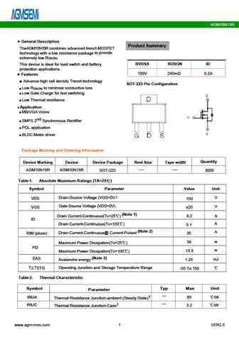
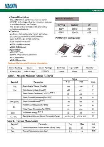
AGM10N15R General Description Product Summary TheAGM10N15R combines advanced trench MOSFET to provide technology with a low resistance package extremely low R DS(ON) This device is ideal and battery BVDSS RDSON ID for load switch protection applications. 150V 245m 8.2A Features Advance high cell density Trench technology SOT-223 Pin Configuration Low R to minimize c
6.1. Size:1557K cn agmsemi
agm10n15d.pdf
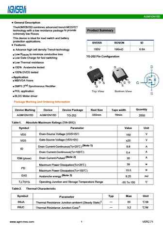
AGM10N15D General Description TheAGM10N15D combines advanced trench MOSFET to provide technology with a low resistance package Product Summary extremely low R DS(ON) This device is ideal and battery for load switch protection applications. BVDSS RDSON ID Features 150V 196m 8.6A Advance high cell density Trench technology Low R to minimize conductive loss DS(ON)
8.1. Size:815K cn agmsemi
agm10n65f.pdf
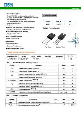
AGM10N65F Table 3. Electrical Characteristics (TJ=25 unless otherwise noted) Symbol Parameter Conditions Min Typ Max Unit On/Off States BVDSS Drain-Source Breakdown Voltage V =0V I =250 A GS D 650 -- -- V Zero Gate Voltage Drain Current V =650V,V =0V -- -- 1 A DS GS I DSS Gate-Body Leakage Current V = 30V,V =0V -- -- nA GS DS I GSS 100 VGS(th) Gate Threshold Voltage
9.1. Size:1274K cn agmsemi
agm1010a-e.pdf
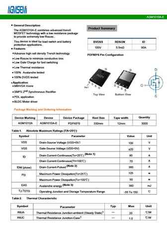
AGM1010A-E TYPICAL ELECTRICAL AND THERMAL CHARACTERISTICS VDS 90% 10% VGS Td(on) Tr Td(off) Tf Ton Toff Fig.7 Switching Time Waveform Fig.8 Gate Charge Waveform www.agm-mos.com 4 VER2.72 AGM1010A-E PDFN5*6 Marking Instructions Model1 Model2 www.agm-mos.com 6 VER2.72 AGM1010A-E Disclaimer The information provided in this document is believed to be accurate and relia
9.2. Size:2622K cn agmsemi
agm1095mn.pdf
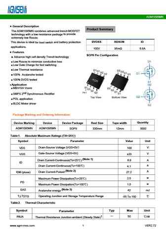
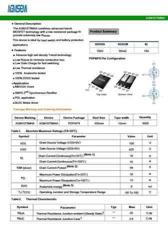
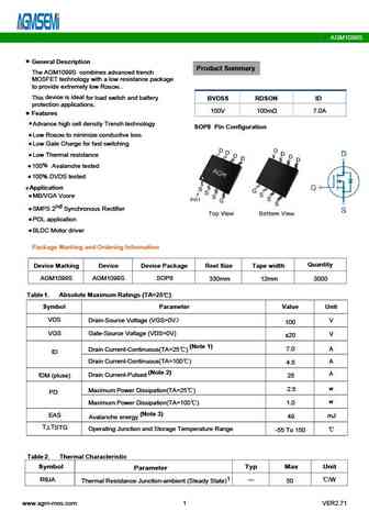
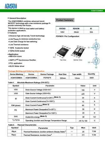
AGM1095MN General Description Product Summary The AGM1095MN combines advanced trench MOSFET to provide technology with a low resistance package extremely low R DS(ON) BVDSS RDSON ID This device is ideal for load switch and battery protection applications. 100V 95m 6.8A Features SOP8 Pin Configuration Advance high cell density Trench technology Low R to minimize cond
9.3. Size:2690K cn agmsemi
agm1075mbp.pdf
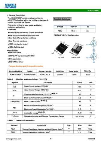
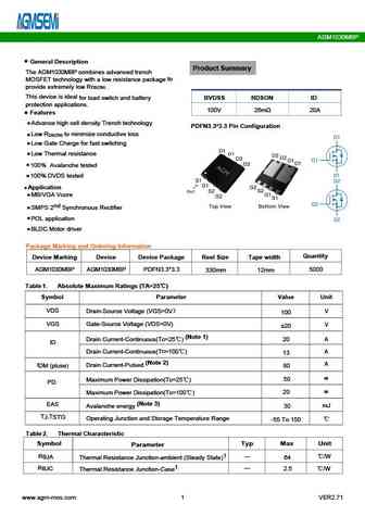
AGM1075MBP General Description The AGM1075MBP combines advanced trench Product Summary to MOSFET technology with a low resistance package provide extremely low R . DS(ON) This device is ideal for load switch and battery BVDSS RDSON ID protection applications. Features 100V 65m 12A Advance high cell density Trench technology PDFN3.3*3.3 Pin Configuration Low R to
9.4. Size:1005K cn agmsemi
agm1075-g.pdf
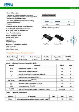
AGM1075-G Typical Performance Characteristics Figure 1. Output Characteristics Figure 2. Transfer Characteristics Figure 3. Drain-to-Source On Resistance Figure 4. Body Diode Forward Voltage vs Drain Current vs Source Current and Temperature Figure 5. Capacitance Characteristics Figure 6. Gate Charge Characteristics www.agm-mos.com 3 VER2.71 AGM1075-G SOT23-3 Marking Inst
9.5. Size:1116K cn agmsemi
agm1075d.pdf
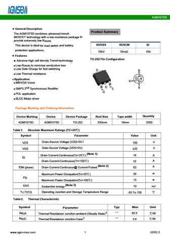
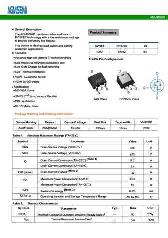
AGM1075D General Description Product Summary The AGM1075D combines advanced trench to MOSFET technology with a low resistance package provide extremely low R DS(ON) BVDSS RDSON ID This device is ideal for load switch and battery protection applications. 100V 55m 16A Features TO-252 Pin Configuration Advance high cell density Trench technology Low R to minimize cond
9.6. Size:2784K cn agmsemi
agm1030ma.pdf
AGM1030MA Table 3. N- Channel Electrical Characteristics (TJ=25 unless otherwisenoted) Symbol Parameter Conditions Min Typ Max Unit On/Off States BV Drain-Source Breakdown Voltage V =0V I =250 A 100 -- -- V GS D DSS Zero Gate Voltage Drain Current V =100V,V =0V -- -- 1 A DS GS I DSS Gate-Body Leakage Current V = 20V,V =0V -- -- nA GS DS 100 I GSS VGS(th) Gate Threshold
9.7. Size:1646K cn agmsemi
agm1099e.pdf
AGM1099E Table 3. Electrical Characteristics (TJ=25 unless otherwise noted) Symbol Parameter Conditions Min Typ Max Unit On/Off States BV Drain-Source Breakdown Voltage V =0V I =250 A 100 -- -- V GS D DSS Zero Gate Voltage Drain Current V =100V,V =0V -- -- 1 A DS GS I DSS V = 20V,V =0V -- -- nA GS DS IGSS Gate-Body Leakage Current 100 VGS(th) Gate Threshold Voltage
9.8. Size:1521K cn agmsemi
agm1095map.pdf
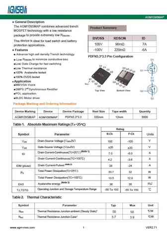
AGM1095MAP General Description The AGM1095MAP combines advanced trench Product Summary MOSFET technology with a low resistance to provide extremely low R . package DS(ON) BVDSS RDSON ID device is This ideal for load switch and battery 100V 96m 7A protection applications. Features -100V 220m -6A Advance high cell density Trench technology PDFN3.3*3.3 Pin Configurat
9.9. Size:1291K cn agmsemi
agm1099ey.pdf
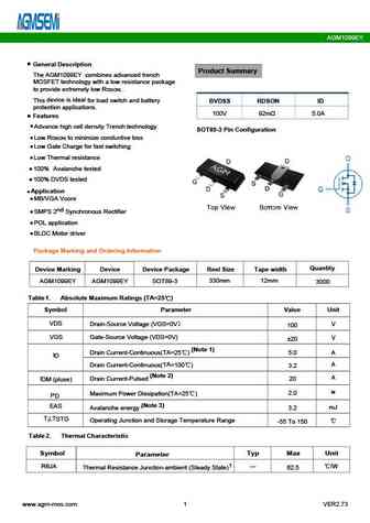
AGM1099EY General Description Product Summary The AGM1099EY combines advanced trench MOSFET technology with a low resistance package to provide extremely low R . DS(ON) device is ideal This for load switch and battery BVDSS RDSON ID protection applications. 100V 92m 5.0A Features Advance high cell density Trench technology SOT89-3 Pin Configuration Low R to mi
9.10. Size:2996K cn agmsemi
agm1075mna.pdf
AGM1075MNA Typical Characteristics (TJ =25 Noted) www.agm-mos.com 3 VER2.71 AGM1075MNA Typical Characteristics (TJ =25 Noted) www.agm-mos.com 4 VER2.71 AGM1075MNA Dimensions PDFN5*6 D3 D MILLIMETER SYMBOL MIN Typ. MAX A 0.900 1.000 1.100 A1 0.254 REF. A2 0 0.05 D 4.824 4.900 4.976 D1 1.605 1.705 1.805 D2 0.500 0.600 0.700 D3 4.924 5.000 5.076 E 5.924 6.000
9.11. Size:1770K cn agmsemi
agm1095m.pdf
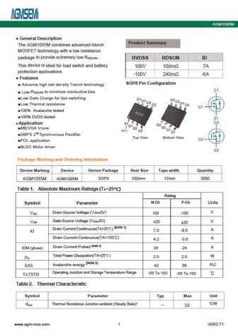
AGM1095M General Description Product Summary The AGM1095M combines advanced trench MOSFET technology with a low resistance to provide extremely low R . package DS(ON) BVDSS RDSON ID device is This ideal for load switch and battery 100V 100m 7A protection applications. -100V 240m -6A Features SOP8 Pin Configuration Advance high cell density Trench technology R to
9.12. Size:1137K cn agmsemi
agm1099el.pdf
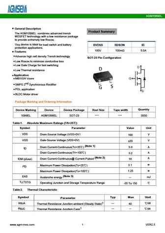
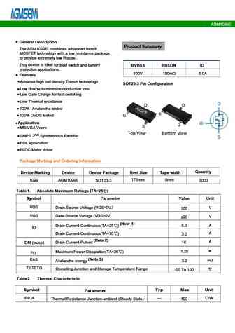
AGM1099EL General Description Product Summary The AGM1099EL combines advanced trench MOSFET technology with a low resistance package to provide extremely low R . DS(ON) device is ideal This for load switch and battery BVDSS RDSON ID protection applications. 100V 100m 5.0A Features Advance high cell density Trench technology SOT-23 Pin Configuration Low R to mi
9.13. Size:989K cn agmsemi
agm1075s.pdf
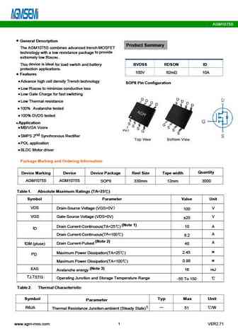
AGM1075S General Description Product Summary The AGM1075S combines advanced trench MOSFET to provide technology with a low resistance package extremely low R . DS(ON) device is ideal This for load switch and battery BVDSS RDSON ID protection applications. 100V 62m 10A Features Advance high cell density Trench technology SOP8 Pin Configuration Low R to minimize
9.14. Size:1510K cn agmsemi
agm1099s.pdf
AGM1099S General Description Product Summary The AGM1099S combines advanced trench MOSFET technology with a low resistance package to provide extremely low R . DS(ON) device is ideal This for load switch and battery BVDSS RDSON ID protection applications. 100V 100m 7.0A Features Advance high cell density Trench technology SOP8 Pin Configuration Low R to minimi
9.15. Size:1466K cn agmsemi
agm1099d.pdf
AGM1099D Characteristics Curve Typ. output characteristics Typ. drain-source on resistance I =f(V ) R =f(I ) D DS DS(on) D Typ. transfer characteristics Drain-source on-state resistance I =f(V ) R =f(T );I =6A; V =10V D GS DS(on) j D GS www.agm-mos.com 3 VER2.73 AGM1099D Gate Threshold Voltage Drain-source breakdown voltage V =f(T ); I =250uA V =f(T ); I =250uA TH j D BR
9.16. Size:1677K cn agmsemi
agm1030mbp.pdf
AGM1030MBP General Description Product Summary The AGM1030MBP combines advanced trench to MOSFET technology with a low resistance package provide extremely low R . DS(ON) This device is ideal for load switch and battery BVDSS RDSON ID protection applications. 100V 26m 20A Features Advance high cell density Trench technology PDFN3.3*3.3 Pin Configuration Low R t
9.17. Size:1039K cn agmsemi
agm1075mn.pdf
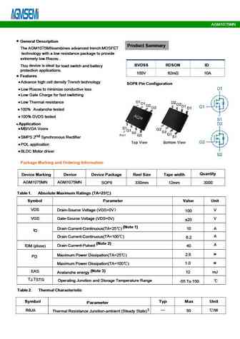
AGM1075MN Test Circuit 1 EAS test circuit 2 Gate charge test circuit 3 Switch Time Test Circuit www.agm-mos.com 3 VER2.55 AGM1075MN Typical Electrical and Thermal Characteristics (curves) Figure1. Source-Drain Diode Forward Voltage Figure2. Safe operating area Figure3. Output characteristics Figure4. Transfer characteristics Figure5. Static drain-source on resistance F
9.18. Size:1651K cn agmsemi
agm1010a-f.pdf
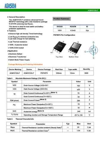
AGM1010A-F Table 3. Electrical Characteristics (TJ=25 unless otherwise noted) Symbol Parameter Conditions Min Typ Max Unit On/Off States BVDSS Drain-Source Breakdown Voltage V =0V I =250 A GS D 100 -- -- V Zero Gate Voltage Drain Current V =100V,V =0V -- -- 1 A DS GS I DSS Gate-Body Leakage Current V = 20V,V =0V -- -- nA GS DS I GSS 100 VGS(th) Gate Threshold Voltag
9.19. Size:1733K cn agmsemi
agm1030mna.pdf
AGM1030MNA Table 3. Electrical Characteristics (TJ=25 unless otherwise noted) Symbol Parameter Conditions Min Typ Max Unit On/Off States BV Drain-Source Breakdown Voltage V =0V I =250 A 100 -- -- V GS D DSS Zero Gate Voltage Drain Current V =100V,V =0V -- -- 1 A DS GS I DSS V = 20V,V =0V -- -- nA GS DS IGSS Gate-Body Leakage Current 100 VGS(th) Gate Threshold Voltag
9.20. Size:1178K cn agmsemi
agm1010a2.pdf
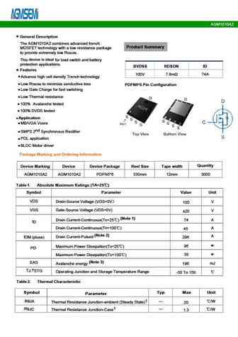
AGM1010A2 Table 3. Electrical Characteristics (TJ=25 unless otherwise noted) Symbol Parameter Conditions Min Typ Max Unit On/Off States BV Drain-Source Breakdown Voltage V =0V I =250 A 100 -- -- V GS D DSS Zero Gate Voltage Drain Current V =100V,V =0V -- -- 1 A DS GS I DSS V = 20V,V =0V -- -- nA GS DS IGSS Gate-Body Leakage Current 100 VGS(th) Gate Threshold Voltage
Otros transistores... AGM085N10C, AGM085N10C1, AGM085N10F, AGM08T15C, AGM1010A2, AGM1010A-E, AGM1010A-F, AGM1030MA, AON6380, AGM10N65F, AGM12N10A, AGM12N10AP, AGM12N10D, AGM12N10MNA, AGM12T02LL, AGM12T05A, AGM12T05C
