AGM13T05A Datasheet. Equivalente. Reemplazo. Hoja de especificaciones. Principales características
Número de Parte: AGM13T05A 📄📄
Tipo de FET: MOSFET
Polaridad de transistor: N
ESPECIFICACIONES MÁXIMAS
Pdⓘ - Máxima disipación de potencia: 105 W
|Vds|ⓘ - Voltaje máximo drenador-fuente: 140 V
|Vgs|ⓘ - Voltaje máximo fuente-puerta: 20 V
|Id|ⓘ - Corriente continua de drenaje: 120 A
Tjⓘ - Temperatura máxima de unión: 150 °C
CARACTERÍSTICAS ELÉCTRICAS
trⓘ - Tiempo de subida: 5 nS
Cossⓘ - Capacitancia de salida: 730 pF
RDSonⓘ - Resistencia estado encendido drenaje a fuente: 0.0075 Ohm
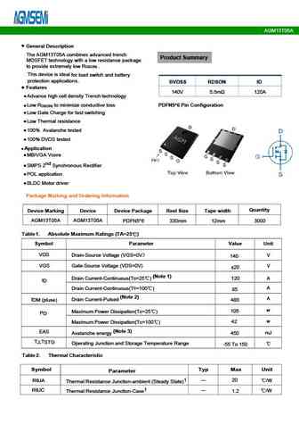
Encapsulados: PDFN5X6
📄📄 Copiar
Búsqueda de reemplazo de AGM13T05A MOSFET
- Selecciónⓘ de transistores por parámetros
AGM13T05A datasheet
agm13t05a.pdf
AGM13T05A Table 3. Electrical Characteristics (TJ=25 unless otherwise noted) Symbol Parameter Conditions Min Typ Max Unit On/Off States BV Drain-Source Breakdown Voltage V =0V I =250 A 140 GS D DSS 145 -- V Zero Gate Voltage Drain Current V =135V,V =0V -- -- 1 A DS GS I DSS V = 20V,V =0V -- -- nA GS DS IGSS Gate-Body Leakage Current 100 VGS(th) Gate Threshold Voltag
agm13t15a.pdf
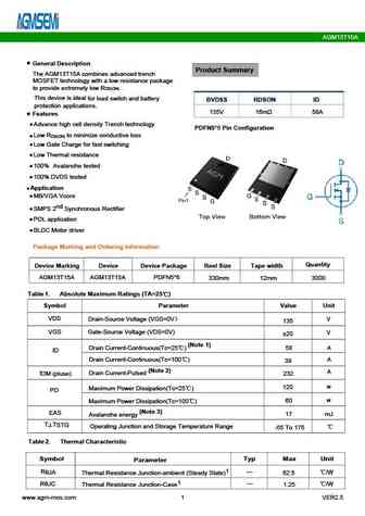
AGM13T15A General Description Product Summary The AGM13T15A combines advanced trench MOSFET technology with a low resistance package to provide extremely low R . DS(ON) This device is ideal for load switch and battery BVDSS RDSON ID protection applications. 135V 16m 58A Features Advance high cell density Trench technology PDFN5*6 Pin Configuration Low R to mi
agm13t15d.pdf
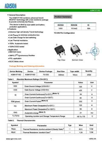
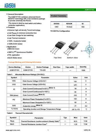
AGM13T15D General Description Product Summary The AGM13T15D combines advanced trench MOSFET technology with a low resistance package to provide extremely low R . DS(ON) This device is ideal for load switch and battery BVDSS RDSON ID protection applications. 135V 15.5m 58A Features Advance high cell density Trench technology TO-252 Pin Configuration Low R to m
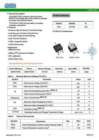
agm13t30a.pdf
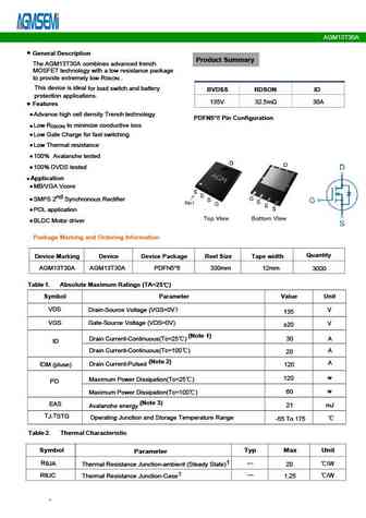
AGM13T30A Test Circuit 1) E test Circuit AS 2) Gate charge test Circuit 3) Switch Time Test Circuit www.agm-mos.com 3 VER2.55 AGM13T30A Typical Electrical and Thermal Characteristics Vds Drain-Source Voltage (V) T J-Junction Temperature( ) Figure 1 Output Characteristics Figure 4 Rdson-Junction Temperature Vgs Gate-Source Voltage (V) Qg Gate Charge (nC) Figure 2 Transfer Chara
Otros transistores... AGM12T02LL, AGM12T05A, AGM12T05C, AGM12T05F, AGM12T08A, AGM12T12A, AGM12T12C, AGM12T12D, CS150N04A8, AGM15T05LL, AGM15T06C, AGM15T06C-B, AGM15T06H, AGM15T06LL, AGM15T06T, AGM15T13A, AGM15T13C
Parámetros del MOSFET. Cómo se afectan entre sí.
History: IRFF9133 | AGM15T13F | KXF2955 | DHFSJ11N65 | IPB65R660CFDA | SI4430BDY | S85N16RP
🌐 : EN ES РУ

Liste
Recientemente añadidas las descripciónes de los transistores:
MOSFET: CS95118 | CS85105A | CS75N45 | CS72N12 | CS55N50 | CS48N75A | CS40N27 | MSQ60P04D | MSQ40P07D | MSQ30P40D | MSQ30P15 | MSQ30P07D | MSQ100N03D | MSHM60P14 | MSHM40N085 | MSHM30N46
Popular searches
irfb438 | mj21193g | irf3710 pinout | irf9530 datasheet | mj21194 | oc71 transistor | 2n3440 | bc550c