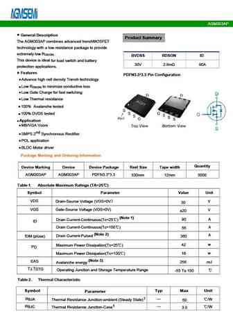
AGM303AP Datasheet. Equivalente. Reemplazo. Hoja de especificaciones. Principales características
Número de Parte: AGM303AP 📄📄
Tipo de FET: MOSFET
Polaridad de transistor: N
ESPECIFICACIONES MÁXIMAS
Pdⓘ - Máxima disipación de potencia: 42 W
|Vds|ⓘ - Voltaje máximo drenador-fuente: 30 V
|Vgs|ⓘ - Voltaje máximo fuente-puerta: 20 V
|Id|ⓘ - Corriente continua de drenaje: 90 A
Tjⓘ - Temperatura máxima de unión: 150 °C
CARACTERÍSTICAS ELÉCTRICAS
trⓘ - Tiempo de subida: 5.7 nS
Cossⓘ - Capacitancia de salida: 380 pF
RDSonⓘ - Resistencia estado encendido drenaje a fuente: 0.0037 Ohm
Encapsulados: PDFN3.3X3.3
📄📄 Copiar
Búsqueda de reemplazo de AGM303AP MOSFET
- Selecciónⓘ de transistores por parámetros
AGM303AP datasheet
agm303ap.pdf
AGM303AP Typical Characteristics VDS, Drain -Source Voltage (V) Tj - Junction Temperature ( C) Fig1. Typical Output Characteristics Fig2. V Gate -Source Voltage Vs.Tj GS(TH) VGS, Gate -Source Voltage (V) Tj - Junction Temperature ( C) Fig3. Typical Transfer Characteristics Fig4. Normalized On-Resistance Vs. Tj VSD, Source-Drain Voltage (V) VDS, Drain -Source Voltage (V) Fig5. Typica
agm303a.pdf
AGM303A V =10V GS V =4.5V GS Fig.3 Threshold Voltage V.S Junction Temperature Fig.4 Resistance V.S Drain Current Fig.5 On-Resistance VS Gate Source Voltage Fig.6 On-Resistance V.S Junction Temperature www.agm-mos.com 3 VER2.72 AGM303A Fig.9 Switching Time Measurement Circuit Fig.10 Gate Charge Waveform Fig.11 Avalanche Measurement Circuit Fig.12 Avalanche Waveform www.agm-mos.com
agm303d1.pdf
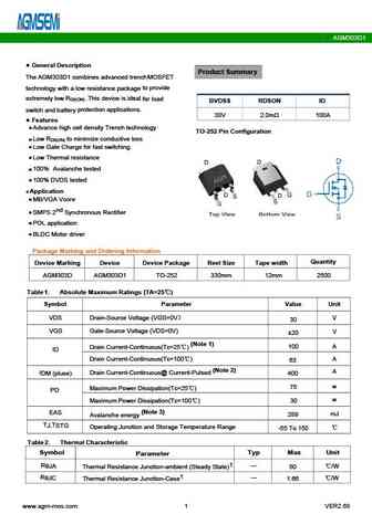
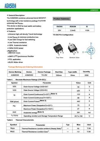
AGM303D1 General Description Product Summary The AGM303D1 combines advanced trenchMOSFET to provide technology with a low resistance package extremely low R .This device is ideal DS(ON) for load BVDSS RDSON ID protection applications. switch and battery 30V 2.0m 100A Features Advance high cell density Trench technology TO-252 Pin Configuration Low R to minimize
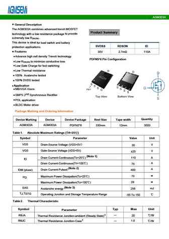
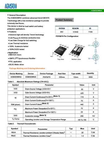
agm303mna.pdf
AGM303MNA V =10V GS V =4.5V GS Fig.3 Threshold Voltage V.S Junction Temperature Fig.4 Resistance V.S Drain Current Fig.5 On-Resistance VS Gate Source Voltage Fig.6 On-Resistance V.S Junction Temperature www.agm-mos.com 3 VER2.5 AGM303MNA Fig.9 Switching Time Measurement Circuit Fig.10 Gate Charge Waveform Fig.11 Avalanche Measurement Circuit Fig.12 Avalanche Waveform www.agm-mos.c
Otros transistores... AGM15T13H, AGM15T16C, AGM15T16D, AGM16N10C, AGM16N10D, AGM302C1, AGM302D1, AGM303A, IRF730, AGM303D, AGM303D1, AGM303MNA, AGM3045A, AGM304A, AGM304A-B, AGM304AP, AGM304AP-B
Parámetros del MOSFET. Cómo se afectan entre sí.
History: AGM304A | AO4832 | AGM150P10S
🌐 : EN ES РУ

Liste
Recientemente añadidas las descripciónes de los transistores:
MOSFET: CS95118 | CS85105A | CS75N45 | CS72N12 | CS55N50 | CS48N75A | CS40N27 | MSQ60P04D | MSQ40P07D | MSQ30P40D | MSQ30P15 | MSQ30P07D | MSQ100N03D | MSHM60P14 | MSHM40N085 | MSHM30N46
Popular searches
bcy21 | s8550 datasheet | mj50ac100 | 2sc1318 replacement | 2n3905 | mj15023 | tip36c transistor | 2sc3320