AGM307MNQ MOSFET Equivalente. Reemplazo. Hoja de especificaciones. Principales características
Número de Parte: AGM307MNQ
Tipo de FET: MOSFET
Polaridad de transistor: N
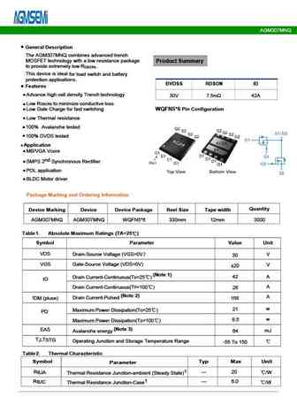
ESPECIFICACIONES MÁXIMAS
Pdⓘ - Máxima disipación de potencia: 21 W
|Vds|ⓘ - Voltaje máximo drenador-fuente: 30 V
|Vgs|ⓘ - Voltaje máximo fuente-puerta: 20 V
|Id|ⓘ - Corriente continua de drenaje: 42 A
Tjⓘ - Temperatura máxima de unión: 150 °C
CARACTERÍSTICAS ELÉCTRICAS
trⓘ - Tiempo de subida: 5 nS
Cossⓘ - Capacitancia de salida: 140 pF
RDSonⓘ - Resistencia estado encendido drenaje a fuente: 0.011 Ohm
Encapsulados: WQFN5X6
Búsqueda de reemplazo de AGM307MNQ MOSFET
- Selecciónⓘ de transistores por parámetros
AGM307MNQ datasheet
agm307mnq.pdf
AGM307MNQ Typical Characteristics VDS, Drain -Source Voltage (V) Tj - Junction Temperature ( C) Fig1. Typical Output Characteristics Fig2. Threshold Voltage Vs. Temperature VGS, Gate -Source Voltage (V) Tj - Junction Temperature ( C) Fig3. Typical Transfer Characteristics Fig4. Normalized On-Resistance Vs. Temperature VSD, Source-Drain Voltage (V) VDS, Drain -Source Voltage
agm307mbp.pdf
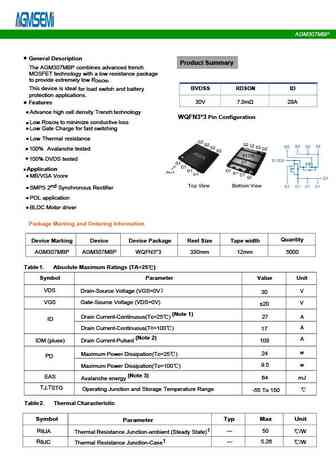
AGM307MBP Table 3. Electrical Characteristics (TJ=25 unless otherwise noted) Symbol Parameter Conditions Min Typ Max Unit On/Off States BVDSS Drain-Source Breakdown Voltage V =0V I =250 A 30 -- -- V GS D Zero Gate Voltage Drain Current V =30V,V =0V -- -- 1 A DS GS I DSS V = 20V,V =0V -- -- nA GS DS IGSS Gate-Body Leakage Current 100 VGS(th) Gate Threshold Voltage V =V
agm308ma.pdf
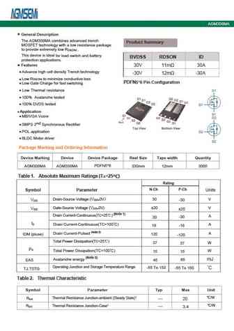
AGM308MA Table 3. N- Channel Electrical Characteristics (TJ=25 unless otherwisenoted) Symbol Parameter Conditions Min Typ Max Unit On/Off States BV Drain-Source Breakdown Voltage V =0V I =250 A 30 -- -- V GS D DSS Zero Gate Voltage Drain Current V =30V,V =0V -- -- 1 A DS GS I DSS Gate-Body Leakage Current V = 20V,V =0V -- -- nA GS DS 100 I GSS VGS(th) Gate Threshold Vo
agm303d1.pdf
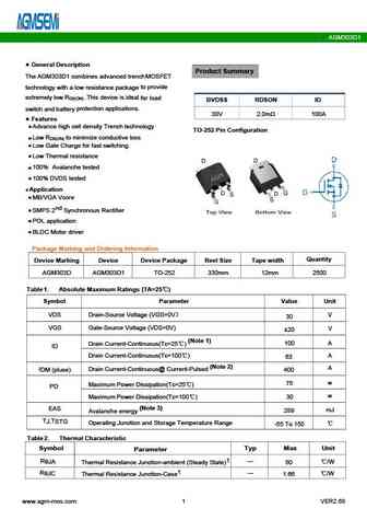
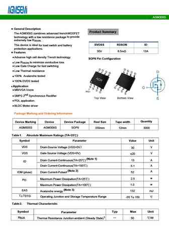
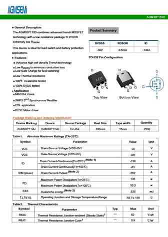
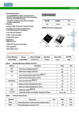
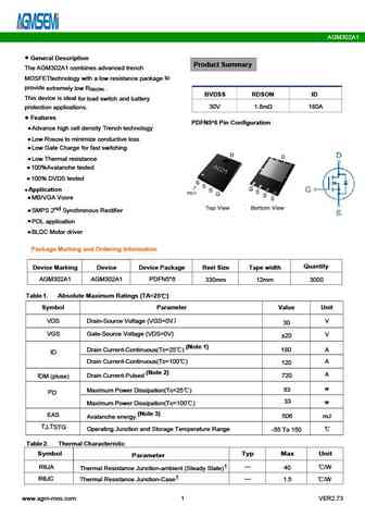
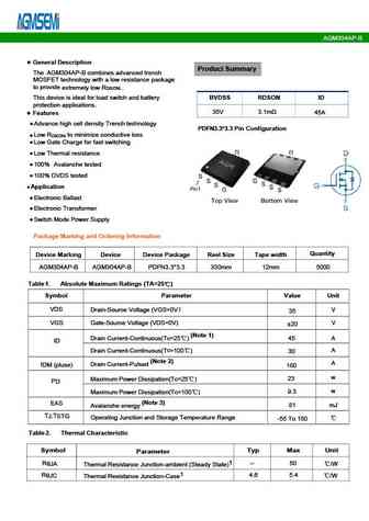
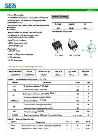
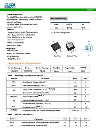
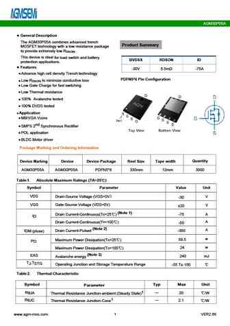
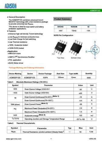
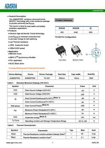
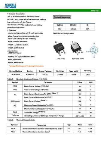
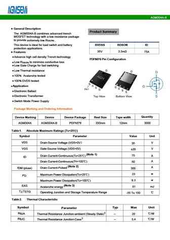
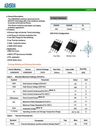
AGM303D1 General Description Product Summary The AGM303D1 combines advanced trenchMOSFET to provide technology with a low resistance package extremely low R .This device is ideal DS(ON) for load BVDSS RDSON ID protection applications. switch and battery 30V 2.0m 100A Features Advance high cell density Trench technology TO-252 Pin Configuration Low R to minimize
agm305ap.pdf
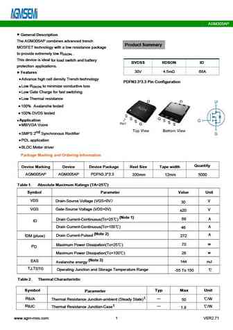
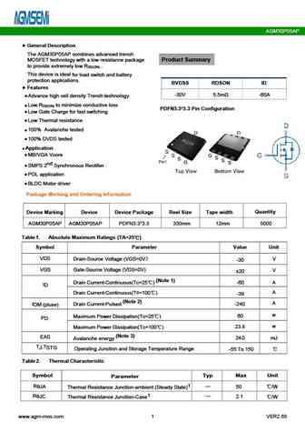
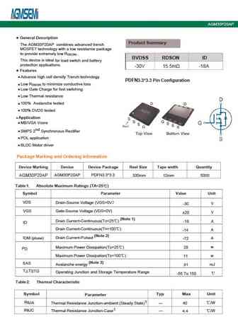
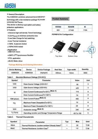
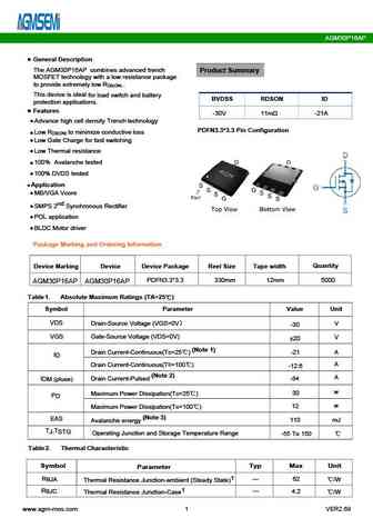
AGM305AP General Description The AGM305AP combines advanced trench Product Summary MOSFET technology with a low resistance package to provide extremely low R . DS(ON) This device is ideal for load switch and battery BVDSS RDSON ID protection applications. 30V 4.5m 68A Features Advance high cell density Trench technology PDFN3.3*3.3 Pin Configuration Low R to
agm30p25mbp.pdf
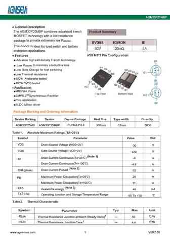
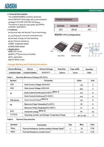
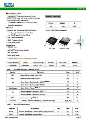
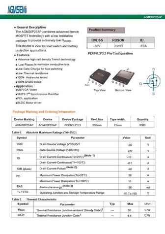
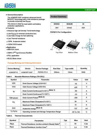
AGM30P25MBP General Description The AGM30P25MBP combines advanced trench Product Summary MOSFET technology with a low resistance to provide extremely low R . package DS(ON) BVDSS RDSON ID This device is ideal for load switch and battery -30V 20m -8A protection applications. Features PDFN3*3 Pin Configuration Advance high cell density Trench technology R to minimize c
agm3015h.pdf
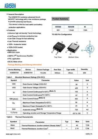
AGM3015H General Description The AGM3015H combines advanced trench Product Summary MOSFET technology with a low resistance package to provide extremely low R . DS(ON) This device is ideal for load switch and battery BVDSS RDSON ID protection applications. 30V 1.5m 138A Features Advance high cell density Trench technology TO-263 Pin Configuration Low R to mini
agm30p25s.pdf
AGM30P25S Characteristics Curve Typ. output characteristics Typ. drain-source on resistance I =f(V ) R =f(I ) D DS DS(on) D Typ. transfer characteristics Drain-source on-state resistance I =f(V ) R =f(T );I =-5A; V =-10V D GS DS(on) j D GS www.agm-mos.com 3 VER2.5 AGM30P25S Gate Threshold Voltage Drain-source breakdown voltage -V =f(T ); I =-250uA V =f(T ); I =-250uA TH
agm306mnq.pdf
AGM306MNQ Table 3. Electrical Characteristics (TJ=25 unless otherwise noted) Symbol Parameter Conditions Min Typ Max Unit On/Off States BVDSS Drain-Source Breakdown Voltage V =0V I =250 A GS D 30 -- -- V Zero Gate Voltage Drain Current V =30V,V =0V -- -- 1 A DS GS I DSS Gate-Body Leakage Current V = 20V,V =0V -- -- nA GS DS I GSS 100 VGS(th) Gate Threshold Voltage V
agm30p10a.pdf
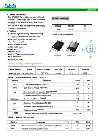
AGM30P10A Fig.1 Power Dissipation Derating Curve Fig.2 Typical output Characteristics 1.2 50 VGS=-10V 1 40 0.8 30 VGS=-4.5V 0.6 20 0.4 10 0.2 0 0 0.5 1 0 Drain-Source voltage (V) 0 50 100 150 200 Temperature ( C) Fig.3 Threshold Voltage V.S Junction Temperature Fig.4 Resistance V.S Drain Current Junction Temperature 30 -50 50 150 0 20 -0.
agm308mn.pdf
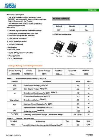
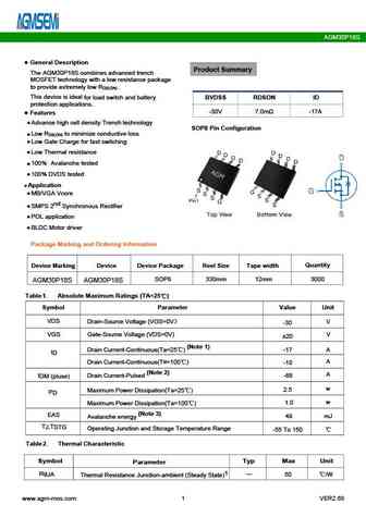
AGM308MN General Description The AGM308MN combines advanced trench Product Summary MOSFET technology with a low resistance package to provide extremely low R . DS(ON) This device is ideal for load switch and battery protection applications. BVDSS RDSON ID Features 30V 8.8m 15A Advance high cell density Trench technology Low R to minimize conductive loss DS(ON)
agm305a.pdf
AGM305A Typical electrical and thermal characteristics Figure 2 Typical Transfer Characteristics Figure 1 Typical Output Characteristics Figure 4 On-Resistance vs. Junction Figure 3 Body-Diode Characteristics Temperature Figure 5 Capacitance Characteristics Figure 6 Gate-Charge Characteristics www.agm-mos.com 3 VER2.72 AGM305A Test circuits and Waveforms Gate charge cir
agm30p12d.pdf
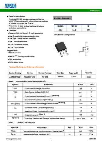
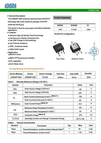
AGM30P12D General Description Product Summary The AGM30P12D combines advanced trench MOSFET technology with a low resistance package to provide extremely low R . DS(ON) This device is ideal for load switch and battery BVDSS RDSON ID protection applications. -30V 11m -35A Features Advance high cell density Trench technology TO-252 Pin Configuration Low R to minim
agm306ap.pdf
AGM306AP Typical Characteristics 12 12 VGS=10V ID=12A VGS=7V 10 VGS=5V 11 8 VGS=4.5V VGS=3V 9 6 4 8 2 6 0 2 4 6 8 10 0 0.25 0.5 0.75 VGS (V) VDS Drain-to-Source Voltage (V) Fig.1 Typical Output Characteristics Fig.2 On-Resistance vs. Gate-Source 10 12 VDS=20V ID=12A 10 8 8 6 TJ=150 TJ=25 6 4 4 2 2 0 0 0 0.3 0.6 0.9 0 6 12 18 24 30 QG , Total Gate
agm304mnq.pdf
AGM304MNQ Typical Characteristics Fig.1 Typical Output Characteristics Fig.2 On-Resistance vs G-S Voltage Fig.3 Source Drain Forward Characteristics Fig.4 Gate-Charge Characteristics 1.8 1.8 1.4 1.4 1.0 1 0.6 0.6 0.2 0.2 -50 0 50 100 150 -50 0 50 100 150 TJ ,Junction Temperature ( ) TJ , Junction Temperature ( ) Fig.5 Normalized V vs T Fig.6 Normalized R vs T GS(th)
agm30p25mbq.pdf
AGM30P25MBQ Table 2. P-Channel Electrical Characteristics (TJ=25 unless otherwisenoted) Symbol Parameter Conditions Min Typ Max Unit On/Off States BVDSS Drain-Source Breakdown Voltage VGS=0V ID=-250 A -30 -- -- V Zero Gate Voltage Drain Current V =-30V,V =0V -1 DS GS I -- -- A DSS Gate-Body Leakage Current V = 20V,V =0V 100 GS DS I -- -- nA GSS V Gate Threshold Voltage V
agm308s.pdf
AGM308S Fig.1 Power Dissipation Fig.2 Typical output Characteristics V =10V GS V =4.5V GS Fig.3 Threshold Voltage V.S Junction Temperature Fig.4 Resistance V.S Drain Current Fig.5 On-Resistance VS Gate Source Voltage Fig.6 On-Resistance V.S Junction Temperature www.agm-mos.com 3 VER2.71 AGM308S Fig.7 Switching Time Measurement Circuit Fig.8 Gate Charge Waveform Fig.9 Switching Tim
agm30p05ap.pdf
AGM30P05AP General Description The AGM30P05AP combines advanced trench Product Summary MOSFET technology with a low resistance package to provide extremely low R . DS(ON) This device is ideal for load switch and battery protection applications. BVDSS RDSON ID Features -30V 5.5m -60A Advance high cell density Trench technology Low R to minimize conductive loss D
agm304ap.pdf
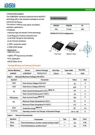
AGM304AP General Description The AGM304AP combines advanced trench Product Summary MOSFETtechnology with a low resistance package to provide extremely low R . DS(ON) This device is ideal for load switch and battery BVDSS RDSON ID protection applications. 30V 3.8m 40A Features Advance high cell density Trench technology PDFN3.3*3.3 Pin Configuration Low R to mi
agm30p20m.pdf
AGM30P20M Characteristics Curve Typ. output characteristics Typ. drain-source on resistance -I =f(-V ) R =f(-I ) D DS DS(on) D Typ. transfer characteristics Drain-source on-state resistance -I =f(-V ) R = f(T ); I =-8A; V =-10V D GS DS(on) j D GS www.agm-mos.com 3 VER2.7 AGM30P20M Gate Threshold Voltage Drain-source breakdown voltage -V =f(T ); I =-250uA -V =f(T ); I =-2
agm30p110d.pdf
AGM30P110D Table 3. Electrical Characteristics (TJ=25 unless otherwise noted) Symbol Parameter Conditions Min Typ Max Unit On/Off States BVDSS Drain-Source Breakdown Voltage V =0V I =-250 A -30 -- -- V GS D Zero Gate Voltage Drain Current V =-30V,V =0V -- -- -1 A DS GS I DSS Gate-Body Leakage Current V = 20V,V =0V -- -- 100 nA GS DS I GSS VGS(th) Gate Threshold Voltage
agm308a.pdf
AGM308A Typical Performance Characteristics Figure 2 Typical Transfer Characteristics Figure1 Output Characteristics ID (A) ID (A) 100 100 10V 8V 80 80 3.5V 5V 60 60 40 40 3V 125 25 20 20 VGS=2.5V VGS(V) VDS(V) 0 0 0 2.0 4.0 6.0 8.0 10.0 0 1 2 3 4 5 6 Figure 3 On-resistance vs. Drain Current Figure 4 Body Diode Characteristics IS(A) RDS(ON) (m ) 14 10
agm30p35s.pdf
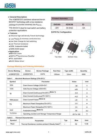
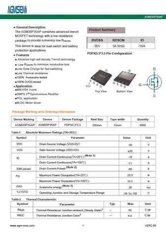
AGM30P35S General Description Product Summary The AGM30P35S combines advanced trench MOSFET technology with a low resistance to provide extremely low R . BVDSS RDSON ID package DS(ON) This device is ideal for load switch and battery -30V 34.5m -6A protection applications. SOP8 Pin Configuration Features Advance high cell density Trench technology R to minimize conduct
agm302c1.pdf
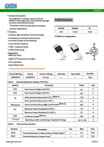
AGM302C1 General Description The AGM302C1 combines advanced trench Product Summary MOSFET technology with a low resistance package to provide extremely low R . DS(ON) This device is ideal for load switch and battery BVDSS RDSON ID protection applications. Features 30V 1.8m 138A Advance high cell density Trench technology TO-220 Pin Configuration Low R to minimi
agm30p35m.pdf
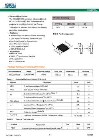
AGM30P35M General Description Product Summary The AGM30P35M combines advanced trench MOSFET technology with a low resistance to provide extremely low R . BVDSS RDSON ID package DS(ON) This device is ideal for load switch and battery -30V 33m -5.4A protection applications. Features SOP8 Pin Configuration Advance high cell density Trench technology R to minimize conduct
agm30p100d.pdf
AGM30P100D Typical Characteristics -VDS,- Drain -Source Voltage (V) Tj - Junction Temperature ( C) Fig1. Typical Output Characteristics Fig2. -V Gate -Source Voltage Vs.Tj GS(TH) -VGS, -Gate -Source Voltage (V) Tj - Junction Temperature ( C) Fig3. Typical Transfer Characteristics Fig4. Normalized On-Resistance Vs. Tj -VSD, -Source-Drain Voltage (V) -VDS, -Drain -Source Vo
agm306d.pdf
AGM306D Test Circuit 1) EAS Test Circuits 2) Gate Charge Test Circuit 3) Switch Time Test Circuit www.agm-mos.com 3 VER2.71 AGM306D TYPICAL ELECTRICAL AND THERMAL CHARACTERISTICS (Curves) Figure 1. Output Characteristics Figure 2. Transfer Characteristics VDS Drain-to-Source Voltage(V) VGS Gate-to-Source Voltage(V) Figure 3. Max BV vs Junction Temperature Figure 4. Drain Curren
agm30p25ap.pdf
AGM30P25AP Table 2. P-Channel Electrical Characteristics (TJ=25 unless otherwisenoted) Symbol Parameter Conditions Min Typ Max Unit On/Off States BVDSS Drain-Source Breakdown Voltage VGS=0V ID=-250 A -30 -- -- V Zero Gate Voltage Drain Current V =-30V,V =0V -1 DS GS I -- -- A DSS Gate-Body Leakage Current V = 20V,V =0V 100 GS DS I -- -- nA GSS V Gate Threshold Voltage V
agm306mbq.pdf
AGM306MBQ Table 3. Electrical Characteristics (T =25 unless otherwise noted) J Symbol Parameter Conditions Min Typ Max Unit On/Off States BV Drain-Source Breakdown Voltage V =0V I =250 A 30 -- -- V GS D DSS Zero Gate Voltage Drain Current V =30V,V =0V -- -- 1 A DS GS I DSS Gate-Body Leakage Current V = 20V,V =0V -- -- nA GS DS I GSS 100 V Gate Threshold Voltage V =V
agm3045a.pdf
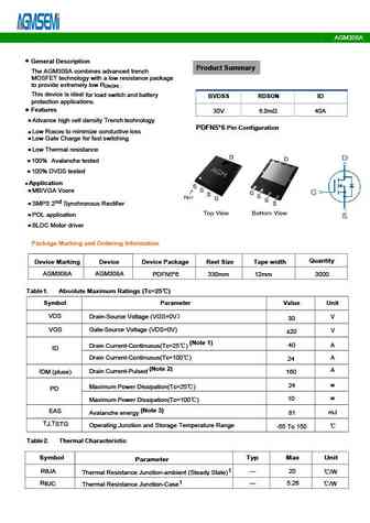
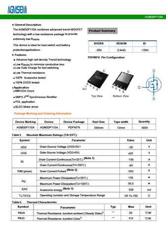
AGM3045A General Description Product Summary The AGM3045A combines advanced trench MOSFET to technology with a low resistance package provide extremely low R . DS(ON) BVDSS RDSON ID This device is ideal load switch and battery protection for applications. 30V 4.6m 80A Features Advance high cell density Trench technology PDFN5*6 Pin Configuration Low R to mini
agm306c.pdf
AGM306C General Description Product Summary The AGM306C combines advanced trenchMOSFET to provide technology with a low resistance package extremely low R . DS(ON) This device is ideal BVDSS RDSON ID for load switch and battery protection applications. 30V 5.7m 60A Features Advance high cell density Trench technology TO-220 Pin Configuration Low R to minimize c
agm304a.pdf
AGM304A General Description Product Summary The AGM304A combines advanced trench MOSFET to provide technology with a low resistance package extremely low R . DS(ON) This device is ideal for load switch and battery BVDSS RDSON ID protection applications. 30V 2.8m 100A Features PDFN5*6 Pin Configuration Advance high cell density Trench technology Low R to minimi
agm306mna.pdf
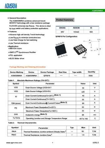
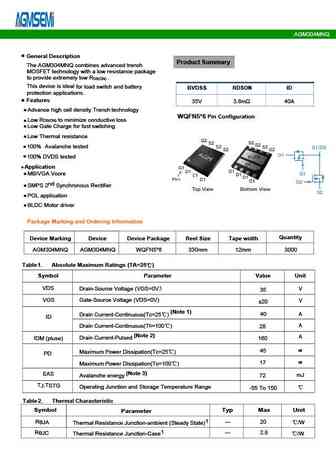
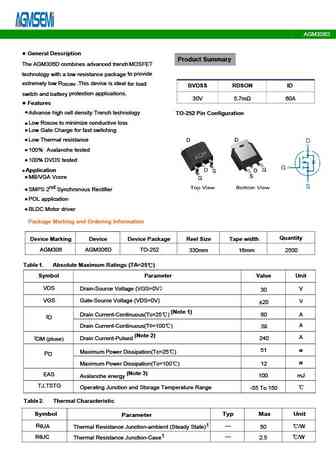
AGM306MNA General Description Product Summary The AGM306MNA combines advanced trench MOSFET technology with a low resistance package to provide extremely low R . This device is ideal DS(ON) BVDSS RDSON ID switch and battery protection applications. for load Features 30V 6.8m 40A Advance high cell density Trench technology QFN5*6 Pin Configuration Low R to minim
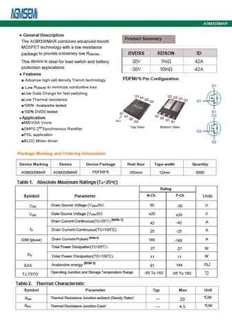
agm308mar.pdf
AGM308MAR Table 3. N- Channel Electrical Characteristics (TJ=25 unless otherwisenoted) Symbol Parameter Conditions Min Typ Max Unit On/Off States BV Drain-Source Breakdown Voltage V =0V I =250 A 30 -- -- V GS D DSS Zero Gate Voltage Drain Current V =30V,V =0V -- -- 1 A DS GS I DSS Gate-Body Leakage Current V = 20V,V =0V -- -- nA GS DS 100 I GSS VGS(th) Gate Threshold V
agm303mna.pdf
AGM303MNA V =10V GS V =4.5V GS Fig.3 Threshold Voltage V.S Junction Temperature Fig.4 Resistance V.S Drain Current Fig.5 On-Resistance VS Gate Source Voltage Fig.6 On-Resistance V.S Junction Temperature www.agm-mos.com 3 VER2.5 AGM303MNA Fig.9 Switching Time Measurement Circuit Fig.10 Gate Charge Waveform Fig.11 Avalanche Measurement Circuit Fig.12 Avalanche Waveform www.agm-mos.c
agm30p100a.pdf
AGM30P100A Typical Characteristics -VDS,- Drain -Source Voltage (V) Tj - Junction Temperature ( C) Fig1. Typical Output Characteristics Fig2. -V Gate -Source Voltage Vs.Tj GS(TH) -VGS, -Gate -Source Voltage (V) Tj - Junction Temperature ( C) Fig3. Typical Transfer Characteristics Fig4. Normalized On-Resistance Vs. Tj -VSD, -Source-Drain Voltage (V) -VDS, -Drain -Source Vo
agm30p85d.pdf
AGM30P85D Table 3. Electrical Characteristics (TJ=25 unless otherwise noted) Symbol Parameter Conditions Min Typ Max Unit On/Off States BV Drain-Source Breakdown Voltage V =0V I =250 A -30 -- -- V GS D DSS Zero Gate Voltage Drain Current V =-30V,V =0V -- -- -1.0 A DS GS I DSS V = 20V,V =0V -- -- nA GS DS IGSS Gate-Body Leakage Current 100 V Gate Threshold Voltage V
agm303ap.pdf
AGM303AP Typical Characteristics VDS, Drain -Source Voltage (V) Tj - Junction Temperature ( C) Fig1. Typical Output Characteristics Fig2. V Gate -Source Voltage Vs.Tj GS(TH) VGS, Gate -Source Voltage (V) Tj - Junction Temperature ( C) Fig3. Typical Transfer Characteristics Fig4. Normalized On-Resistance Vs. Tj VSD, Source-Drain Voltage (V) VDS, Drain -Source Voltage (V) Fig5. Typica
agm3015d.pdf
AGM3015D Typical Electrical and Thermal Characteristics (Curves) Vds Drain-Source Voltage (V) TJ-Junction Temperature( ) Figure 1 Output Characteristics Figure 4 Rdson-JunctionTemperature Vgs Gate-Source Voltage (V) Qg Gate Charge (nC) Figure 2 Transfer Characteristics Figure 5 Gate Charge ID- Drain Current (A) Vsd Source-Drain Voltage (V) Figure 3 Rdson- Drain Current Figure 6
agm3015a.pdf
AGM3015A Typical Electrical & Thermal Characteristics 150 30 VGS = 10V VGS = 3.5V VDS = 5.0V VGS = 5.0V VGS = 4.5V 120 24 VGS = 4.0V TJ = 125 C 90 18 60 12 VGS = 3.0V TJ = 25 C 30 6 VGS = 2.7V VGS = 2.5V 0 0 0 0.6 1.2 1.8 2.4 3 1 1.5 2 2.5 3 3.5 VDS (V) VGS (V) Figure 1 Saturation Characteristics Figure 2 Transfer Characteristics 4 2.5 3.2 2 VGS = 10V ID = 20A VG
agm308mbp.pdf
AGM308MBP Table 3. Electrical Characteristics (TJ=25 unless otherwise noted) Symbol Parameter Conditions Min Typ Max Unit On/Off States BVDSS Drain-Source Breakdown Voltage V =0V I =250 A 30 -- -- V GS D Zero Gate Voltage Drain Current V =30V,V =0V -- -- 1 A DS GS I DSS V = 20V,V =0V -- -- nA GS DS IGSS Gate-Body Leakage Current 100 VGS(th) Gate Threshold Voltage V =V
agm30p18s.pdf
AGM30P18S General Description Product Summary The AGM30P18S combines advanced trench MOSFET technology with a low resistance package to provide extremely low R . DS(ON) This device is ideal for load switch and battery BVDSS RDSON ID protection applications. -30V 7.0m -17A Features Advance high cell density Trench technology SOP8 Pin Configuration Low R to minimi
agm30p35ap.pdf
AGM30P35AP General Description Product Summary The AGM30P35AP combines advanced trench MOSFET technology with a low resistance to provide extremely low R . BVDSS RDSON ID package DS(ON) This device is ideal for load switch and battery -30V 34.5m -16A protection applications. PDFN3.3*3.3 Pin Configuration Features Advance high cell density Trench technology R to minimi
agm304s.pdf
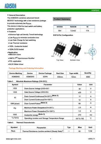
AGM304S General Description The AGM304S combines advanced trench Product Summary MOSFET technology with a low resistance package to provide extremely low R . DS(ON) This device is ideal for load switch and battery BVDSS RDSON ID protection applications. 30V 5.2m 17A Features Advance high cell density Trench technology SOP-8 Pin Configuration Low R to minimize
agm30p08ap.pdf
AGM30P08AP P- Channel Typical Characteristics TC=25 impulse=250uS -4.5V -6V -10V -3.5V 25 -3V -2.5 V -Vds Drain-Source Voltage (V) -Vgs Gate-Source Voltage (V) Figure 1. On-Region Characteristics Figure 2. Transfer Characteristics Note TJ=25 VGS= 0V 25 VGS= -4.5V VGS= -10V -ID - Drain Current (A) -VF ,Forward Voltage (V) Figure 3. On-Resistance Variation vs F
agm301c1.pdf
AGM301C1 General Description The AGM301C1 combines advanced trench Product Summary MOSFET technology with a low resistance package to provide extremely low R . DS(ON) This device is ideal for load switch and battery BVDSS RDSON ID protection applications. Features 30V 1.5m 170A Advance high cell density Trench technology TO-220 Pin Configuration Low R to minim
agm3005a.pdf
AGM3005A General Description Product Summary The AGM3005A combines advanced trenchMOSFET to provide technology with a low resistance package extremely low R . DS(ON) This device is ideal BVDSS RDSON ID for load switch and battery protection applications. 30V 0.5m 316A Features Advance high cell density Trench technology PDFN5*6 Pin Configuration Low R to minimi
agm30p20d.pdf
AGM30P20D Table 3. Electrical Characteristics (TJ=25 unless otherwise noted) Symbol Parameter Conditions Min Typ Max Unit On/Off States BVDSS Drain-Source Breakdown Voltage V =0V I =-250 A -30 -- -- V GS D Zero Gate Voltage Drain Current V =-30V,V =0V -- -- -1 A DS GS I DSS Gate-Body Leakage Current V = 20V,V =0V -- -- 100 nA GS DS I GSS VGS(th) Gate Threshold Voltage
agm302a1.pdf
AGM302A1 General Description Product Summary The AGM302A1 combines advanced trench to MOSFETtechnology with a low resistance package provide extremely low R . DS(ON) BVDSS RDSON ID This device is ideal for load switch and battery 30V 1.8m 180A protection applications. Features PDFN5*6 Pin Configuration Advance high cell density Trench technology Low R to min
agm302d1.pdf
AGM302D1 General Description Product Summary The AGM302D1 combines advanced trenchMOSFET to provide technology with a low resistance package extremely low R .This device is ideal DS(ON) for load BVDSS RDSON ID protection applications. switch and battery 30V 2.1m 180A Features Advance high cell density Trench technology TO-252 Pin Configuration Low R to minimize
agm30p08d.pdf
AGM30P08D Table 3. Electrical Characteristics (TJ=25 unless otherwise noted) Symbol Parameter Conditions Min Typ Max Unit On/Off States BV Drain-Source Breakdown Voltage V =0V I =250 A -30 -- -- V GS D DSS Zero Gate Voltage Drain Current V =-30V,V =0V -- -- -1.0 A DS GS I DSS V = 20V,V =0V -- -- nA GS DS IGSS Gate-Body Leakage Current 100 V Gate Threshold Voltage V
agm30p25m.pdf
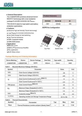
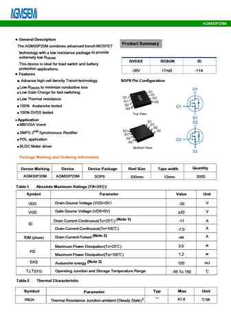
AGM30P25M General Description Product Summary The AGM30P25M combines advanced trench MOSFET technology with a low resistance to provide extremely low R . BVDSS RDSON ID package DS(ON) This device is ideal for load switch and battery -30V 22m -8A protection applications. SOP8 Pin Configuration Features Advance high cell density Trench technology R to minimize conductiv
agm304ap-b.pdf
AGM304AP-B TYPICAL ELECTRICAL AND THERMAL CHARACTERIS Figure 2 Transfer Characteristics (Note E) Figure 1 On-Region Characteristics (Note E) Figure 4 On-Resistance vs. Junction Figure 3 On-Resistance vs. Drain Current and Gate Voltage (Note E) Temperature (Note E) Figure 5 On-Resistance vs. Gate-Source Figure 6 Body-Diode Characteristics (Note E) Voltage (Note E) www.agm
agm30p10sr.pdf
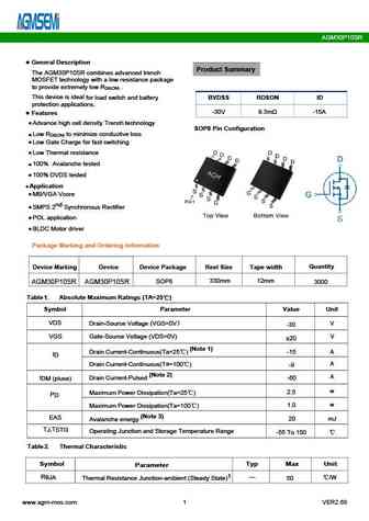
AGM30P10SR General Description Product Summary The AGM30P10SR combines advanced trench MOSFET technology with a low resistance package to provide extremely low R . DS(ON) This device is ideal for load switch and battery BVDSS RDSON ID protection applications. -30V 9.3m -15A Features Advance high cell density Trench technology SOP8 Pin Configuration Low R to mini
agm30p25d.pdf
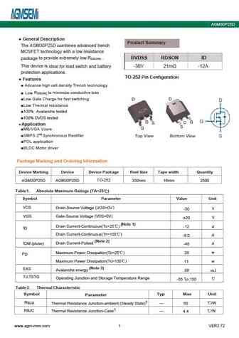
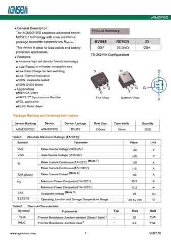
AGM30P25D General Description Product Summary The AGM30P25D combines advanced trench MOSFET technology with a low resistance to provide extremely low R . BVDSS RDSON ID package DS(ON) This device is ideal for load switch and battery -30V 21m -12A protection applications. TO-252 Pin Configuration Features Advance high cell density Trench technology R to minimize conduc
agm30p110a.pdf
AGM30P110A Table 3. Electrical Characteristics (TJ=25 unless otherwise noted) Symbol Parameter Conditions Min Typ Max Unit On/Off States BVDSS Drain-Source Breakdown Voltage V =0V I =-250 A -30 -- -- V GS D Zero Gate Voltage Drain Current V =-30V,V =0V -- -- -1 A DS GS I DSS Gate-Body Leakage Current V = 20V,V =0V -- -- 100 nA GS DS I GSS VGS(th) Gate Threshold Voltage
agm30p16s.pdf
AGM30P16S Ciss Vgs Coss Crss Qg Vds Fig.3 Power Dissipation Derating Curve Fig.4 Typical output Characteristics V =-10V GS V =-4.5V GS Fig.5 Threshold Voltage V.S Junction Temperature Fig.6 Resistance V.S Drain Current www.agm-mos.com 3 VER2.68 AGM30P16S Fig.9 Switching Time Measurement Circuit Fig.10 Gate Charge Waveform Fig.11 Switching Time Measurement Circuit Fig.12 Gate
agm30p55d1.pdf
AGM30P55D1 General Description Product Summary The AGM30P55D1 combines advanced trench MOSFET technology with a low resistance package to provide extremely low R . DS(ON) This device is ideal for load switch and battery BVDSS RDSON ID protection applications. -30V 6.5m -65A Features Advance high cell density Trench technology TO-252 Pin Configuration Low R to mi
agm30p12m.pdf
AGM30P12M Fig.1 Power Dissipation Derating Curve Fig.2 Typical output Characteristics 1.2 50 VGS=-10V 1 40 0.8 30 VGS=-4.5V 0.6 20 0.4 10 0.2 0 0 0.5 1 0 Drain-Source voltage (V) 0 50 100 150 200 Temperature ( C) Fig.3 Threshold Voltage V.S Junction Temperature Fig.4 Resistance V.S Drain Current Junction Temperature 30 -50 50 150 0 20 -0.
agm30p14mbp.pdf
AGM30P14MBP -Vds Drain-Source Voltage (V) TJ-Junction Temperature( ) Figure 7 Capacitance vs Vds Figure 9 Power De-rating -Vds Drain-Source Voltage (V) TJ-Junction Temperature( ) Figure 8 Safe Operation Area Figure 10 ID Current Derating Square Wave Pluse Duration(sec) Figure 11 Normalized Maximum Transient Thermal Impedance www.agm-mos.com 4 VER2.68 C Capacitance (pF) Po
agm30p10k.pdf
AGM30P10K Typical Characteristics Power Capability Current Capability 60 55 50 50 45 40 40 35 30 30 25 20 20 15 10 10 5 TC=25oC,VG= -10V TC=25oC 0 0 0 20 40 60 80 100 120 140 160 180 0 20 40 60 80 100 120 140 160 Tmp Mounting Point Temp. ( Tmp Mounting Point Temp. ( C) C) Safe Operating Area Transient Thermal Impedance 100 2 1 Duty = 0.5 1ms 0.2
agm30p20ap.pdf
AGM30P20AP Characteristics Curve www.agm-mos.com 3 VER2.68 AGM30P20AP Figure7 Safe Operation Area Figure8 Normalized Maximum Transient Thermal Impedance www.agm-mos.com 4 VER2.68 AGM30P20AP Dimensions PDFN3.3*3.3 MILLIMETER D SYMBOL MIN Typ. MAX A 0.700 0.800 0.900 b A1 0.152REF. A2 0 0.05 D 3.000 3.100 3.200 D1 2.300 2.450 2.600 D1 E 2.900 3.000 3.100 E1 3.1
agm308ap.pdf
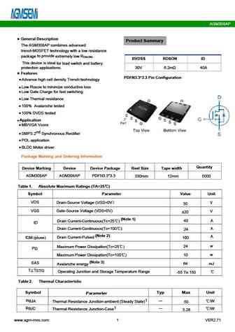
AGM308AP General Description Product Summary The AGM308AP combines advanced trenchMOSFET technology with a low resistance to provide package extremely low R . DS(ON) BVDSS RDSON ID This device is ideal for load switch and battery 30V 6.2m 40A protection applications. Features PDFN3.3*3.3 Pin Configuration Advance high cell density Trench technology Low R to mi
agm305ma.pdf
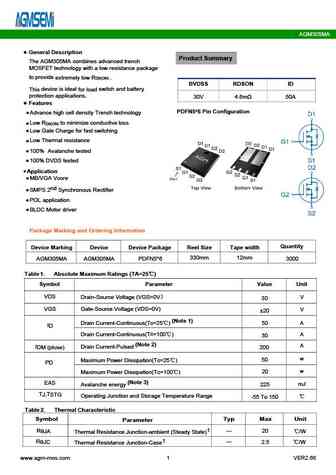
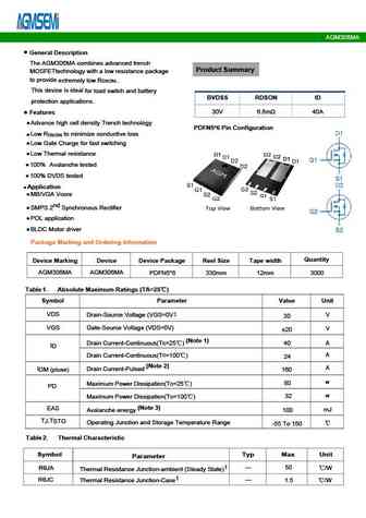
AGM305MA General Description Product Summary The AGM305MA combines advanced trench MOSFET technology with a low resistance package to provide extremely low R . DS(ON) BVDSS RDSON ID switch and battery This device is ideal for load protection applications. 30V 4.6m 50A Features PDFN5*6 Pin Configuration Advance high cell density Trench technology Low R to minim
agm304d.pdf
AGM304D Typical Characteristics TJ = 25 C, unless otherwise noted 120 120 10V 8V 100 100 6V VDS = 15V 4.5V 4V 80 80 3.5V 60 60 40 40 C 20 TJ = 125 20 TJ = 25 C 0 0 0 1 2 3 4 5 0 1 2 3 4 5 6 VDS (Volts) VGS (Volts) Figure 1 On-Region Characteristics Figure 2 Transfer Characteristics 10000 10 9 TJ = 25 C 8 Ciss 1000 7 VGS = 4.5V Co
agm30p10ap.pdf
AGM30P10AP P- Channel Typical Characteristics -3V TC=25 impulse=250uS -3.5V -4.5V 25 -6V -10V -2.5V Vds Drain-Source Voltage (V) -Vgs Gate-Source Voltage (V) Figure 1. On-Region Characteristics Figure 2. Transfer Characteristics VGS= 0V Note TJ=25 VGS=-4.5V 25 VGS=-10V -V F ,Forward Voltage [V] -I D - Drain Current (A) Figure 4. Body Diode Forward Voltage F
agm306ma.pdf
AGM306MA Fig.1 Power Dissipation Derating Curve Fig.2 Typical output Characteristics 1.2 50 1 V =10V GS 0.8 V =4.5V GS 25 0.6 0.4 0.2 0 0 0.5 1 1.5 2 0 Drain-Source voltage (V) 0 50 100 150 200 Temperature ( C) Fig.3 Threshold Voltage V.S Junction Temperature Fig.4 Resistance V.S Drain Current 2.5 20 2 1.5 10 1 0.5 0 0 -50 50 150 0 10 20 30 Junction Tempe
agm30p18e.pdf
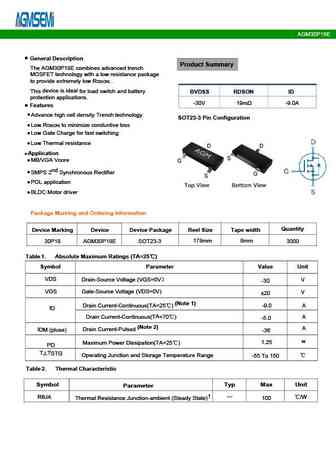
AGM30P18E Table 3. Electrical Characteristics (TA=25 unless otherwise noted) Symbol Parameter Conditions Min Typ Max Unit On/Off States BV Drain-Source Breakdown Voltage V =0V I =250 A -30 -- -- V GS D DSS Zero Gate Voltage Drain Current V =-30V,V =0V -- -- -1 A DS GS I DSS V = 20V,V =0V -- -- nA GS DS IGSS Gate-Body Leakage Current 100 VGS(th) Gate Threshold Voltag
agm3012ap-cp.pdf
AGM3012AP-CP Table 3. Electrical Characteristics (TJ=25 unless otherwise noted) Symbol Parameter Conditions Min Typ Max Unit On/Off States BV Drain-Source Breakdown Voltage V =0V I =250 A 30 35 -- V GS D DSS Zero Gate Voltage Drain Current V =30V,V =0V -- -- 1 A DS GS I DSS V = 20V,V =0V -- -- nA GS DS IGSS Gate-Body Leakage Current 100 VGS(th) Gate Threshold Voltag
agm30p16d.pdf
AGM30P16D Typical Electrical and Thermal Characteristics (Curves) -Vds Drain-Source Voltage (V) TJ-Junction Temperature( ) Figure 1 Output Characteristics Figure 4 Rdson-Junction Temperature Vgs Gate-Source Voltage (V) Qg Gate Charge (nC) Figure 2 Transfer Characteristics Figure 5 Gate Charge -ID- Drain Current (A) Vsd Source-Drain Voltage (V) Figure 3 Rdson- Drain Current Figu
agm30p05d.pdf
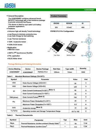
AGM30P05D General Description The AGM30P05D combines advanced trench MOSFET technology with a low resistance package Product Summary to provide extremely low R . DS(ON) This device is ideal for load switch and battery protection applications. BVDSS RDSON ID Features Advance high cell density Trench technology -30V 5.5m -75A Low R to minimize conductive loss DS(
agm306a.pdf
AGM306A Table 3. Electrical Characteristics (T =25 unless otherwise noted) J Symbol Parameter Conditions Min Typ Max Unit On/Off States BV Drain-Source Breakdown Voltage V =0V I =250 A 30 -- -- V GS D DSS Zero Gate Voltage Drain Current V =30V,V =0V -- -- 1 A DS GS I DSS V = 20V,V =0V -- -- nA GS DS IGSS Gate-Body Leakage Current 100 VGS(th) Gate Threshold Voltage V
agm30p05a.pdf
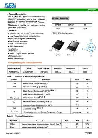
AGM30P05A General Description The AGM30P05A combines advanced trench Product Summary MOSFET technology with a low resistance package to provide extremely low R . DS(ON) This device is ideal for load switch and battery BVDSS RDSON ID protection applications. Features -30V 5.5m -75A Advance high cell density Trench technology PDFN5*6 Pin Configuration Low R to mi
agm303a.pdf
AGM303A V =10V GS V =4.5V GS Fig.3 Threshold Voltage V.S Junction Temperature Fig.4 Resistance V.S Drain Current Fig.5 On-Resistance VS Gate Source Voltage Fig.6 On-Resistance V.S Junction Temperature www.agm-mos.com 3 VER2.72 AGM303A Fig.9 Switching Time Measurement Circuit Fig.10 Gate Charge Waveform Fig.11 Avalanche Measurement Circuit Fig.12 Avalanche Waveform www.agm-mos.com
agm306mbp.pdf
AGM306MBP Table 3. Electrical Characteristics (T =25 unless otherwise noted) J Symbol Parameter Conditions Min Typ Max Unit On/Off States BV Drain-Source Breakdown Voltage V =0V I =250 A 30 -- -- V GS D DSS Zero Gate Voltage Drain Current V =30V,V =0V -- -- 1 A DS GS I DSS Gate-Body Leakage Current V = 20V,V =0V -- -- nA GS DS I GSS 100 V Gate Threshold Voltage V =V
agm30p08a.pdf
AGM30P08A General Description The AGM30P08A combines advanced trench Product Summary MOSFET technology with a low resistance to provide extremely low R . package DS(ON) BVDSS RDSON ID This device is ideal for load switch and battery protection applications. -30V 7.0m -60A Features Advance high cell density Trench technology PDFN5*6 Pin Configuration R to minimize con
agm30p10s.pdf
AGM30P10S General Description Product Summary The AGM30P10S combines advanced trench MOSFET technology with a low resistance package to provide extremely low R . DS(ON) This device is ideal for load switch and battery BVDSS RDSON ID protection applications. -30V 12m -14A Features Advance high cell density Trench technology SOP8 Pin Configuration Low R to minimiz
agm30p55d.pdf
AGM30P55D General Description The AGM30P55D combines advanced trench Product Summary MOSFET technology with a low resistance package to provide extremely low R . DS(ON) This device is ideal for load switch and battery protection applications. BVDSS RDSON ID Features -30V 5m -65A Advance high cell density Trench technology Low R to minimize conductive loss DS(ON)
agm30p16ap.pdf
AGM30P16AP General Description The AGM30P16AP combines advanced trench Product Summary MOSFET technology with a low resistance package to provide extremely low R . DS(ON) This device is ideal for load switch and battery BVDSS RDSON ID protection applications. Features -30V 11m -21A Advance high cell density Trench technology PDFN3.3*3.3 Pin Configuration Low R
agm30p35d.pdf
AGM30P35D General Description Product Summary The AGM30P35D combines advanced trench MOSFET technology with a low resistance to provide extremely low R . BVDSS RDSON ID package DS(ON) This device is ideal for load switch and battery -30V 36.5m -20A protection applications. TO-252 Pin Configuration Features Advance high cell density Trench technology R to minimize cond
agm30p55a.pdf
AGM30P55A Fig.1 Power Dissipation Derating Curve Fig.2 Typical output Characteristics V =-10V GS V =-4.5V GS Fig.3 Threshold Voltage V.S Junction Temperature Fig.4 Resistance V.S Drain Current Fig.5 On-Resistance VS Gate Source Voltage Fig.6 On-Resistance V.S Junction Temperature www.agm-mos.com 3 VER2.68 AGM30P55A Fig.7 Switching Time Measurement Circuit Fig.8 Gate Charge Waveform
agm303d.pdf
AGM303D V =10V GS V =4.5V GS Fig.3 Threshold Voltage V.S Junction Temperature Fig.4 Resistance V.S Drain Current Fig.5 On-Resistance VS Gate Source Voltage Fig.6 On-Resistance V.S Junction Temperature www.agm-mos.com 3 VER2.72 AGM303D Fig.9 Switching Time Measurement Circuit Fig.10 Gate Charge Waveform Fig.11 Avalanche Measurement Circuit Fig.12 Avalanche Waveform www.agm-mos.com
agm30p20s.pdf
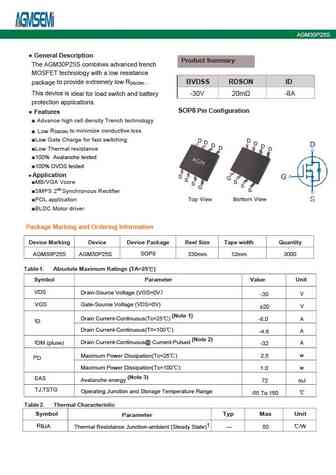
AGM30P20S General Description Product Summary The AGM30P20S combines advanced trench MOSFET to provide technology with a low resistance package extremely low R DS(ON) BVDSS RDSON ID This device is ideal for load switch and battery protection applications. -30V 15.5m -11A Features Advance high cell density Trench technology SOP8 Pin Configuration Low R to minimize co
agm301a1.pdf
AGM301A1 Table 3. Electrical Characteristics (T =25 unless otherwise noted) J Symbol Parameter Conditions Min Typ Max Unit On/Off States BV Drain-Source Breakdown Voltage V =0V I =250 A 30 -- -- V GS D DSS Zero Gate Voltage Drain Current V =30V,V =0V -- -- 1 A DS GS I DSS V = 20V,V =0V -- -- nA GS DS IGSS Gate-Body Leakage Current 100 VGS(th) Gate Threshold Voltage
agm305d.pdf
AGM305D www.agm-mos.com 3 VER2.71 AGM305D TYPICAL ELECTRICAL AND THERMAL CHARACTERISTICS (Curves) Figure 1. Output Characteristics Figure 2. Transfer Characteristics VDS Drain-to-Source Voltage(V) VGS Gate-to-Source Voltage(V) Figure 3. Max BVDSS vs Junction Temperature Figure 4. Drain Current TJ-Junction Temperature( ) TJ-Junction Temperature( ) Figure 5. VGS(th) vs Juncti
agm304a-b.pdf
AGM304A-B TYPICAL ELECTRICAL AND THERMAL CHARACTERIS Figure 2 Transfer Characteristics (Note E) Figure 1 On-Region Characteristics (Note E) Figure 4 On-Resistance vs. Junction Figure 3 On-Resistance vs. Drain Current and Gate Voltage (Note E) Temperature (Note E) Figure 5 On-Resistance vs. Gate-Source Figure 6 Body-Diode Characteristics (Note E) Voltage (Note E) www.agm-
agm308sr.pdf
AGM308SR Fig.1 Power Dissipation Fig.2 Typical output Characteristics 1.2 200 1 150 0.8 V =10V GS 100 0.6 V =4.5V GS 0.4 50 0.2 0 0 0.5 1 1.5 2 0 Drain-Source voltage (V) 0 50 100 150 200 Temperature ( C) Fig.3 Threshold Voltage V.S Junction Temperature Fig.4 Resistance V.S Drain Current 2.5 6 5 2 4 1.5 3 1 2 0.5 1 0 0 0 50 100 -50 50 150 Drain Curren
Otros transistores... AGM306C, AGM306D, AGM306MA, AGM306MBP, AGM306MBQ, AGM306MNA, AGM306MNQ, AGM307MBP, IRF9540N, AGM312M1, AGM312M2, AGM312MAP, AGM312ME, AGM314MA, AGM314MAP, AGM314MD, AGM315MBP
🌐 : EN ES РУ

Liste
Recientemente añadidas las descripciónes de los transistores:
MOSFET: AUP060N055 | AUP056N10 | AUP056N08BGL | AUP052N085 | AUP045N12 | AUP039N10 | AUP034N10 | AUP034N06 | AUP033N08BG | AUP026N085 | AUN084N10 | AUN065N10 | AUN063N10 | AUN062N08BG | AUN060N08AG | AUN053N10
Popular searches
ac176 transistor | mpsa20 | irfp264 | ksc2690 | bc546 datasheet | mpsa06 transistor | tta004b | 2sc1116