AGM6070A Datasheet. Equivalente. Reemplazo. Hoja de especificaciones. Principales características
Número de Parte: AGM6070A 📄📄
Tipo de FET: MOSFET
Polaridad de transistor: N
ESPECIFICACIONES MÁXIMAS
Pdⓘ - Máxima disipación de potencia: 89 W
|Vds|ⓘ - Voltaje máximo drenador-fuente: 60 V
|Vgs|ⓘ - Voltaje máximo fuente-puerta: 20 V
|Id|ⓘ - Corriente continua de drenaje: 76 A
Tjⓘ - Temperatura máxima de unión: 150 °C
CARACTERÍSTICAS ELÉCTRICAS
trⓘ - Tiempo de subida: 7 nS
Cossⓘ - Capacitancia de salida: 290 pF
RDSonⓘ - Resistencia estado encendido drenaje a fuente: 0.009 Ohm
Encapsulados: PDFN5X6
📄📄 Copiar
Búsqueda de reemplazo de AGM6070A MOSFET
- Selecciónⓘ de transistores por parámetros
AGM6070A datasheet
..1. Size:677K cn agmsemi
agm6070a.pdf 

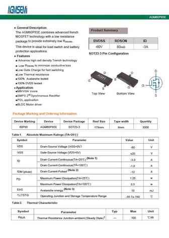
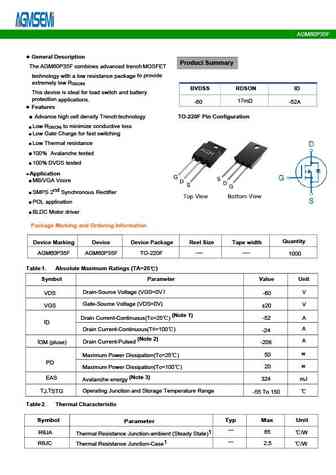
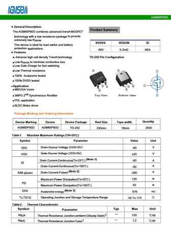
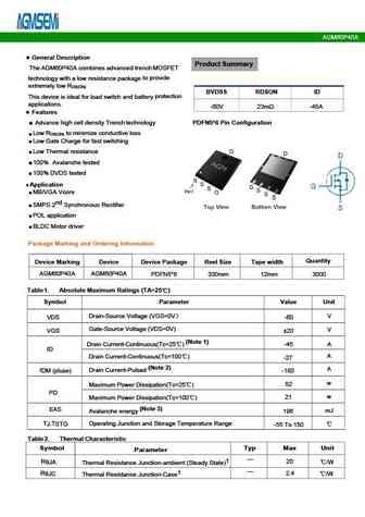
AGM6070A General Description Product Summary The AGM6070A combines advanced trench MOSFET to provide technology with a low resistance package extremely low R . DS(ON) BVDSS RDSON ID This device is ideal for load switch and battery 60V 7.0m 76A protection applications. PDFN5*6 Pin Configuration Features Advance high cell density Trench technology Low R to mini
9.1. Size:1076K cn agmsemi
agm60p85e.pdf
AGM60P85E Figure 7. Gate Charge Waveforms Figure 8. Capacitance Figure 9. Body-Diode Characteristics Figure 10. Maximum Safe Operating Area www.agm-mos.com 4 VER2.65 AGM60P85AP 1) EAS Test Circuits 2) Gate Charge Test Circuit 3) Switch Time Test Circuit www.agm-mos.com 5 VER2.65 AGM60P85E SOT23-3 Marking Instructions www.agm-mos.com 7 VER2.65 AGM60P85E Disclaimer Th
9.2. Size:1659K cn agmsemi
agm60p20ap.pdf
AGM60P20AP Typ. output characteristics Typ. drain-source on resistance -I =f(-V ) R =f(-I ) D DS DS(on) D 200 30 -10V -4.0V -4.5V 25 -5.0V 150 20 -4.5V 15 -5.0V 10 100 -4.0V -10V 5 0 50 0 1 2 3 4 5 0 5 10 15 20 -VDS[V] -ID[A] Typ. transfer characteristics Typ. forward transconductance -I =f(-V ) g =f(-I ) D GS fs D 20 20 15 15 10 10 5 5 0 0 0 1 2 3 4 5
9.3. Size:1728K cn agmsemi
agm609c.pdf

AGM609C General Description Product Summary The AGM609C combines advanced trench MOSFET to provide technology with a low resistance package extremely low R . DS(ON) BVDSS RDSON ID device is ideal This for load switch and battery protection applications. 60V 6.3m 80A Features TO-220 Pin Configuration Advance high cell density Trench technology Low R to minimize
9.4. Size:869K cn agmsemi
agm605f.pdf

AGM605F General Description Product Summary The AGM605F combines advanced trenchMOSFET to provide technology with a low resistance package extremely low R . DS(ON) BVDSS RDSON ID This device is ideal for load switch and battery protection applications. 60V 4.5m 80A Features Advance high cell density Trench technology TO-220F Pin Configuration Low R to minimize
9.5. Size:981K cn agmsemi
agm6035f.pdf

AGM6035F Table 3. Electrical Characteristics (TJ=25 unless otherwise noted) Symbol Parameter Conditions Min Typ Max Unit On/Off States BVDSS Drain-Source Breakdown Voltage V =0V I =250 A 60 -- -- V GS D Zero Gate Voltage Drain Current V =60V,V =0V -- -- 1 A DS GS I DSS Gate-Body Leakage Current V = 20V,V =0V -- -- nA GS DS I GSS 100 V Gate Threshold Voltage V =V ,I =2
9.6. Size:1256K cn agmsemi
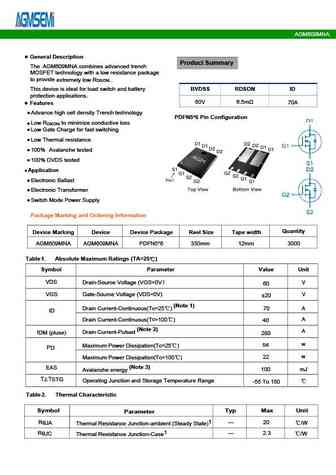
agm609mna.pdf
AGM609MNA 100 14 VDS=5V 10V 8V 12 80 6V 10 VGS=4V 60 8 6 40 4 20 Tj=125 2 VGS=3V Tj=25 0 0 0 1 2 3 4 5 0 1 2 3 4 VDS (V) VGS (V) Fig1. Typical Output Characteristics Fig2. Typical Transfer Characteristics 18 10 15 VGs=10V 12 9 VGs=4.5V 1 6 3 Tj=25 Tj=125 0 0.1 0 25 50 75 100 125 150 175 200 0.0 0.4 0.8 1.2 1.6 Tj-Iunction Temperature ( ) VSD
9.7. Size:1254K cn agmsemi
agm6014a.pdf

AGM6014A Table 3. Electrical Characteristics (TJ=25 unless otherwise noted) Symbol Parameter Conditions Min Typ Max Unit On/Off States BV Drain-Source Breakdown Voltage V =0V I =250 A 60 -- -- V GS D DSS Zero Gate Voltage Drain Current V =60V,V =0V -- -- 1.0 A DS GS I DSS Gate-Body Leakage Current V = 20V,V =0V -- -- nA GS DS I GSS 100 V Gate Threshold Voltage V =V ,
9.8. Size:973K cn agmsemi
agm60p06s.pdf
AGM60P06S P-Channel Typical Characteristics 160 12 ID=-3A VGS=-3V 10 120 8 6 VGS=-10V 4 80 VGS=-7V VGS=-5V 2 VGS=-4.5V 0 40 0 0.5 1 1.5 2 2 4 6 8 10 -VDS , Drain-to-Source Voltage (V) -VGS (V) Fig.1 Typical Output Characteristics Fig.2 On-Resistance v.s Gate-Source 12 10 ID=-3A 10 8 8 6 6 TJ=150 TJ=25 4 4 2 2 0 0 0.2 0.4 0.6 0.8 1 0 5 10 15 20 25 -V
9.9. Size:1260K cn agmsemi
agm6080c.pdf

AGM6080C General Description Product Summary The AGM6080C combines advanced trenchMOSFET to provide technology with a low resistance package extremely low R . DS(ON) BVDSS RDSON ID This device is ideal for load switch and battery protection applications. 60V 7.5m 80A Features Advance high cell density Trench technology TO-220 Pin Configuration Low R to minimiz
9.10. Size:1121K cn agmsemi
agm60p35f.pdf
AGM60P35F Table 3. Electrical Characteristics (TJ=25 unless otherwise noted) Symbol Parameter Conditions Min Typ Max Unit On/Off States BVDSS Drain-Source Breakdown Voltage V =0V I =-250 A -60 -- -- V GS D Zero Gate Voltage Drain Current V =-60V,V =0V -- -- -1 A DS GS I DSS Gate-Body Leakage Current V = 20V,V =0V -- -- 100 nA GS DS I GSS VGS(th) Gate Threshold Voltage
9.11. Size:1473K cn agmsemi
agm609f.pdf

AGM609F General Description Product Summary The AGM609F combines advanced trench MOSFET to provide technology with a low resistance package extremely low R . DS(ON) BVDSS RDSON ID device is ideal This for load switch and battery protection applications. 60V 6.3m 80A Features TO-220F Pin Configuration Advance high cell density Trench technology Low R to minimize
9.12. Size:1316K cn agmsemi
agm60p14a.pdf
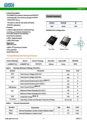
AGM60P14A General Description The AGM60P14A combines advanced trench MOSFET Product Summary to provide technology with a low resistance package extremely low R DS(ON) This device is ideal and battery for load switch BVDSS RDSON ID protection applications. -60V 18m -52A Features Advance high cell density Trench technology PDFN5*6 Pin Configuration Low R to minimize
9.13. Size:1942K cn agmsemi
agm60p100a.pdf
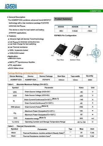
AGM60P100A Table 3. Electrical Characteristics (TJ=25 unless otherwise noted) Symbol Parameter Conditions Min Typ Max Unit On/Off States BVDSS Drain-Source Breakdown Voltage V =0V I =-250 A -60 -- -- V GS D Zero Gate Voltage Drain Current V =-60V,V =0V -- -- -1 A DS GS I DSS Gate-Body Leakage Current V = 20V,V =0V -- -- 100 nA GS DS I GSS VGS(th) Gate Threshold Voltage
9.14. Size:1683K cn agmsemi
agm60p20d.pdf
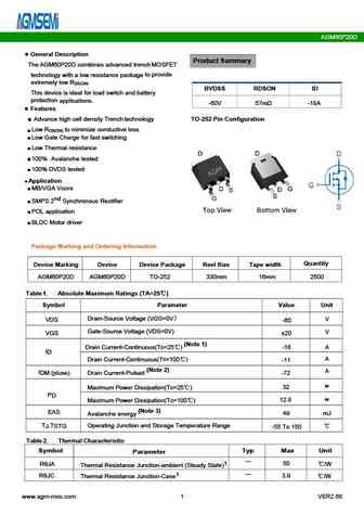
AGM60P20D General Description Product Summary The AGM60P20D combines advanced trench MOSFET to provide technology with a low resistance package extremely low R DS(ON) BVDSS RDSON ID This device is ideal for load switch and battery protection applications. -60V 57m -18A Features Advance high cell density Trench technology TO-252 Pin Configuration Low R to minimize co
9.15. Size:906K cn agmsemi
agm609s.pdf

AGM609S Table 3. Electrical Characteristics (TJ=25 unless otherwise noted) Symbol Parameter Conditions Min Typ Max Unit On/Off States BV Drain-Source Breakdown Voltage V =0V I =250 A 60 -- -- V GS D DSS Zero Gate Voltage Drain Current V =60V,V =0V -- -- 1 A DS GS I DSS Gate-Body Leakage Current V = 20V,V =0V -- -- nA GS DS I GSS 100 V Gate Threshold Voltage V =V ,I =
9.16. Size:1513K cn agmsemi
agm60p20r.pdf
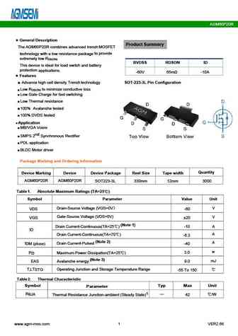
AGM60P20R General Description Product Summary The AGM60P20R combines advanced trench MOSFET to provide technology with a low resistance package extremely low R DS(ON) BVDSS RDSON ID This device is ideal for load switch and battery protection applications. -60V 65m -10A Features Advance high cell density Trench technology SOT-223-3L Pin Configuration Low R to minimiz
9.17. Size:1508K cn agmsemi
agm609d.pdf

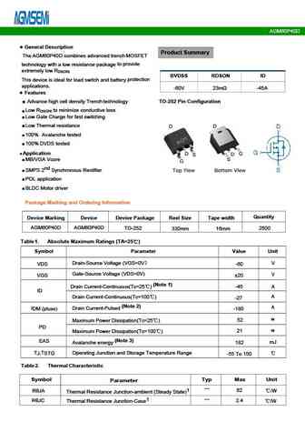
AGM609D General Description Product Summary The AGM609D combines advanced trench MOSFET to provide technology with a low resistance package extremely low R . DS(ON) BVDSS RDSON ID This device is ideal for load switch and battery protection applications. 60V 6.3m 60A Features TO-252 Pin Configuration Advance high cell density Trench technology Low R to minimize
9.18. Size:1214K cn agmsemi
agm60p85d.pdf
AGM60P85D Figure 1. Output Characteristics Figure 2. Transfer Characteristics Figure 3. Power Dissipation Figure 4. Drain Current Figure 5. BV vs Junction Temperature Figure 6. R vs Junction Temperature DSS DS(ON) www.agm-mos.com 3 VER2.65 AGM60P85D Figure 7. Gate Charge Waveforms Figure 8. Capacitance Figure 9. Body-Diode Characteristics Figure 10. Maximum Safe Operating Area
9.19. Size:996K cn agmsemi
agm6080d.pdf

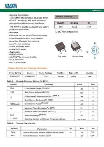
AGM6080D General Description Product Summary The AGM6080D combines advanced trenchMOSFET to provide technology with a low resistance package extremely low R . DS(ON) BVDSS RDSON ID This device is ideal for load switch and battery protection applications. 60V 6.0m 82A Features Advance high cell density Trench technology TO-252 Pin Configuration Low R to minimiz
9.20. Size:1314K cn agmsemi
agm60p30ap.pdf
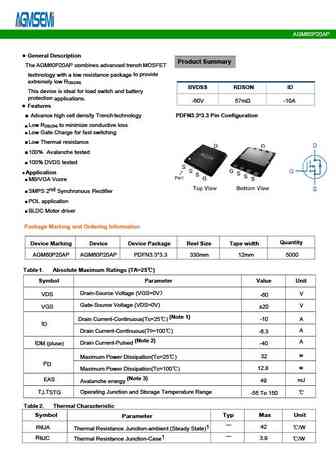
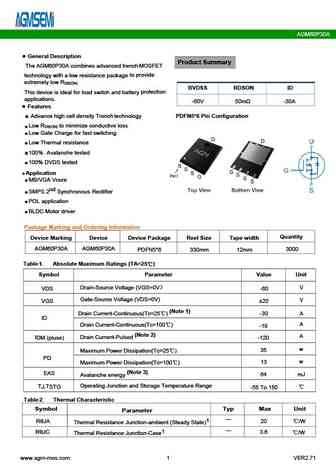
AGM60P30AP General Description Product Summary The AGM60P30AP combines advanced trench MOSFET to provide technology with a low resistance package extremely low R DS(ON) BVDSS RDSON ID This device is ideal for load switch and battery protection applications. -60V 40m -30A Features Advance high cell density Trench technology PDFN3.3*3.3 Pin Configuration Low R to mini
9.21. Size:1595K cn agmsemi
agm60p30c.pdf
AGM60P30C Typical Characteristics (Cont.) Output Characteristics Drain-Source On Resistance 40 35 VGS= -5,-6,-7,-8,-9,-10V 35 -4V 30 30 VGS= -4.5V 25 25 20 20 15 10 VGS= -10V 15 5 -3V 0 10 0.0 0.5 1.0 1.5 2.0 2.5 3.0 0 10 20 30 40 -VDS - Drain-Source Voltage (V) -ID - Drain Current (A) Transfer Characteristics Normalized Threshold Voltage 60 1.8 IDS = -250 A ID
9.22. Size:1410K cn agmsemi
agm602c.pdf

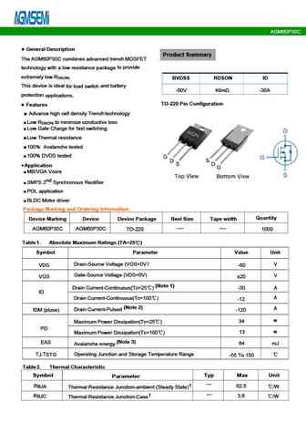
AGM602C General Description Product Summary The AGM602C combines advanced trenchMOSFET to provide technology with a low resistance package extremely low R . DS(ON) BVDSS RDSON ID This device is ideal for load switch and battery protection applications. 60V 2.3m 210A Features Advance high cell density Trench technology TO-220 Pin Configuration Low R to minimize
9.23. Size:3388K cn agmsemi
agm60p90d.pdf
AGM60P90D Typical Characteristics Fig -VDS, -Drain -Source Voltage (V) Tj - Junction Temperature ( C) Fig1. Typical Output Characteristics Fig2. Typical -V Gate -Source Voltage Vs. Tj GS(TH) - - - - Fig Tj - Junction Temperature ( C) -VGS, -Gate -Source Voltage (V) Fig4. Typical Normalized On-Resistance Vs. Tj Fig3. Typical Transfer Characteristics -ID, -Drain-Source Curre
9.24. Size:904K cn agmsemi
agm60p14d.pdf
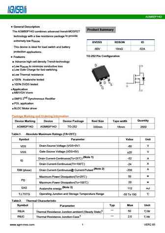
AGM60P14D General Description Product Summary The AGM60P14D combines advanced trench MOSFET to provide technology with a low resistance package extremely low R DS(ON) BVDSS RDSON ID This device is ideal and battery for load switch -60V 18m -52A protection applications. TO-252 Pin Configuration Features Advance high cell density Trench technology Low R to minimize
9.25. Size:1248K cn agmsemi
agm609ap.pdf

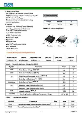
AGM609AP General Description Product Summary The AGM609AP combines advanced Super Trench ll to MOSFET technology with a low resistance package provide extremely low R . DS(ON) BVDSS RDSON ID This device is ideal load switch and battery protection for applications. 60V 7.5m 58A Features Advance high cell density Trench technology PDFN3.3*3.3 Pin Configuration
9.26. Size:1088K cn agmsemi
agm603c.pdf

AGM603C 1000 10 V 5 V 6 V VDS= 10 V 400 7 V Tj = 25 4.5 V 100 300 4 V 10 200 3.5 V 1 100 3 V VGS= 2.5 V 0.1 0 0 2 4 6 8 10 0 1 2 3 4 5 6 7 8 9 10 VDS, Drain-source voltage (V) VGS, Gate-source voltage(V) Figure 1, Typ. output characteristics Figure 2, Typ. transfer characteristics 10.0 105 f = 100 kHz ID = 25 A VGS = 0 V VDS = 30 V 104 7.5 Ciss 103 5.0 C
9.27. Size:1018K cn agmsemi
agm603f.pdf

AGM603F 1000 10 V 5 V 6 V VDS= 10 V 400 7 V Tj = 25 4.5 V 100 300 4 V 10 200 3.5 V 1 100 3 V VGS= 2.5 V 0.1 0 0 2 4 6 8 10 0 1 2 3 4 5 6 7 8 9 10 VDS, Drain-source voltage (V) VGS, Gate-source voltage(V) Figure 1, Typ. output characteristics Figure 2, Typ. transfer characteristics 10.0 105 f = 100 kHz ID = 25 A VGS = 0 V VDS = 30 V 104 7.5 Ciss 103 5.0 C
9.28. Size:1885K cn agmsemi
agm605a.pdf

AGM605A General Description Product Summary The AGM605A combines advanced trenchMOSFET to provide technology with a low resistance package extremely low R . DS(ON) BVDSS RDSON ID This device is ideal for load switch and battery protection applications. 60V 4.4m 80A Features Advance high cell density Trench technology PDFN5*6 Pin Configuration Low R to minimiz
9.29. Size:1268K cn agmsemi
agm6035a.pdf

AGM6035A Table 3. Electrical Characteristics (TJ=25 unless otherwise noted) Symbol Parameter Conditions Min Typ Max Unit On/Off States BVDSS Drain-Source Breakdown Voltage V =0V I =250 A 60 -- -- V GS D Zero Gate Voltage Drain Current V =60V,V =0V -- -- 1 A DS GS I DSS Gate-Body Leakage Current V = 20V,V =0V -- -- nA GS DS I GSS 100 V Gate Threshold Voltage V =V ,I =2
9.30. Size:1175K cn agmsemi
agm60p14ap.pdf
AGM60P14AP General Description The AGM60P14AP combines advanced trench Product Summary to MOSFET technology with a low resistance package provide extremely low R DS(ON) This device is ideal and battery for load switch BVDSS RDSON ID protection applications. Features -60V 18m -52A Advance high cell density Trench technology PDFN3.3*3.3 Pin Configuration Low R to m
9.31. Size:924K cn agmsemi
agm606s.pdf

AGM606S Electrical characteristics diagrams Diagram 2 Max. transient thermal impedance Diagram 1 Power dissipation (SOP-8) (SOP-8) 101 100 0.5 0.3 0.05 10-1 0.02 0.01 0.1 10-2 single pulse 10-3 10-5 10-4 10-3 10-2 10-1 100 101 102 103 tp [s] Ptot=f(TC) ZthJC=f(tp); parameter D= tp/T Diagram 3 Safe operating area (SOP-8) Diagram 4 Typ. gate charge 10 102 10 s
9.32. Size:1232K cn agmsemi
agm603d.pdf

AGM603D Table 3. Electrical Characteristics (TJ=25 unless otherwise noted) Symbol Parameter Conditions Min Typ Max Unit On/Off States BV Drain-Source Breakdown Voltage V =0V I =250 A 60 -- -- V GS D DSS Zero Gate Voltage Drain Current V =60V,V =0V -- -- 1 A DS GS I DSS Gate-Body Leakage Current V = 20V,V =0V -- -- nA GS DS I GSS 100 -- V Gate Threshold Voltage V =V
9.33. Size:1343K cn agmsemi
agm60p30d.pdf
AGM60P30D Table 3. Electrical Characteristics (TJ=25 unless otherwise noted) Symbol Parameter Conditions Min Typ Max Unit On/Off States BVDSS Drain-Source Breakdown Voltage V =0V I =-250 A -60 -- -- V GS D Zero Gate Voltage Drain Current V =-60V,V =0V -- -- -1 A DS GS I DSS Gate-Body Leakage Current V = 20V,V =0V -- -- 100 nA GS DS I GSS VGS(th) Gate Threshold Voltage
9.34. Size:1276K cn agmsemi
agm6018a.pdf

AGM6018A Table 3. Electrical Characteristics (TJ=25 unless otherwise noted) Symbol Parameter Conditions Min Typ Max Unit On/Off States BV Drain-Source Breakdown Voltage V =0V I =250 A 60 -- -- V GS D DSS Zero Gate Voltage Drain Current V =60V,V =0V -- -- 1.0 A DS GS I DSS Gate-Body Leakage Current V = 20V,V =0V -- -- nA GS DS I GSS 100 V Gate Threshold Voltage V =V ,
9.35. Size:1315K cn agmsemi
agm60p40a.pdf
AGM60P40A Table 3. Electrical Characteristics (TJ=25 unless otherwise noted) Symbol Parameter Conditions Min Typ Max Unit On/Off States BVDSS Drain-Source Breakdown Voltage V =0V I =-250 A -60 -- -- V GS D Zero Gate Voltage Drain Current V =-60V,V =0V -- -- -1 A DS GS I DSS Gate-Body Leakage Current V = 20V,V =0V -- -- 100 nA GS DS I GSS VGS(th) Gate Threshold Voltage
9.36. Size:1588K cn agmsemi
agm60p30a.pdf
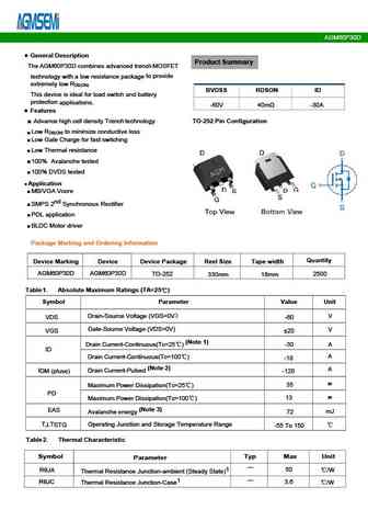
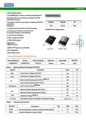
AGM60P30A General Description Product Summary The AGM60P30A combines advanced trench MOSFET to provide technology with a low resistance package extremely low R DS(ON) BVDSS RDSON ID protection This device is ideal for load switch and battery applications. -60V 50m -30A Features Advance high cell density Trench technology PDFN5*6 Pin Configuration Low R to minimize c
9.37. Size:1450K cn agmsemi
agm60p90a.pdf
AGM60P90A Figure 7. Gate Charge Waveforms Figure 8. Capacitance Figure 9. Body-Diode Characteristics Figure 10. Maximum Safe Operating Area www.agm-mos.com 4 VER2.66 AGM60P90A Test Circuit 1) EAS Test Circuits 2) Gate Charge Test Circuit 3) Switch Time Test Circuit www.agm-mos.com 5 VER2.66 AGM60P90A Dimensions PDFN5*6 D2 D MILLIMETER SYMBOL MIN Typ. MAX A 0.
9.38. Size:1166K cn agmsemi
agm605c.pdf

AGM605C General Description Product Summary The AGM605C combines advanced trenchMOSFET to provide technology with a low resistance package extremely low R . DS(ON) BVDSS RDSON ID This device is ideal for load switch and battery protection applications. 60V 4.5m 80A Features Advance high cell density Trench technology TO-220 Pin Configuration Low R to minimize
9.39. Size:934K cn agmsemi
agm601ll.pdf

AGM601LL Table 3. Electrical Characteristics (TJ=25 unless otherwise noted) Symbol Parameter Conditions Min Typ Max Unit On/Off States BV Drain-Source Breakdown Voltage V =0V I =250 A 60 -- -- V GS D DSS Zero Gate Voltage Drain Current V =60V,V =0V -- -- 1 A DS GS I DSS Gate-Body Leakage Current V = 20V,V =0V -- -- nA GS DS I GSS 100 V Gate Threshold Voltage V =V ,I
9.40. Size:1184K cn agmsemi
agm60p85ap.pdf
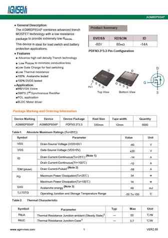
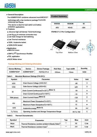
AGM60P85AP General Description Product Summary The AGM60P85AP combines advanced trench MOSFET technology with a low resistance to provide extremely low R . BVDSS RDSON ID package DS(ON) This device is ideal for load switch and battery -60V 80m -14A protection applications. PDFN3.3*3.3 Pin Configuration Features Advance high cell density Trench technology R to minimize
9.41. Size:1169K cn agmsemi
agm6014ap.pdf

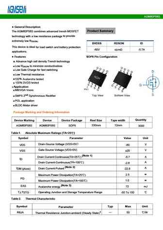
AGM6014AP General Description The AGM6014AP combines advanced trench MOSFET technology with a low resistance package Product Summary to provide extremely low R . DS(ON) device is ideal This for load switch and battery protection applications. BVDSS RDSON ID Features 60V 4.3m 72A Advance high cell density Trench technology Low R to minimize conductive loss DS(ON)
9.42. Size:1299K cn agmsemi
agm608c.pdf

AGM608C General Description Product Summary The AGM608C combines advanced trenchMOSFET to provide technology with a low resistance package extremely low R . DS(ON) BVDSS RDSON ID This device is ideal for load switch and battery protection applications. 60V 4.8m 90A Features Advance high cell density Trench technology TO-220 Pin Configuration Low R to minimize
9.43. Size:1162K cn agmsemi
agm60p40d.pdf
AGM60P40D Typical Characteristics 30 12 ID=-12A 10 28 VGS=-10V 8 VGS=-7V 26 VGS=-5V 6 VGS=-4.5V 24 4 22 VGS=-3V 2 0 20 0 0.25 0.5 0.75 1 2 4 6 8 10 -VDS Drain-to-Source Voltage (V) -VGS (V) Fig.1 Typical Output Characteristics Fig.2 On-Resistance v.s Gate-Source 12 10 VDS=-20V ID=-12A 10 8 8 6 6 TJ=150 TJ=25 4 4 2 2 0 0 0 20 40 60 0.2 0.4 0.6 0.
9.44. Size:1208K cn agmsemi
agm605q.pdf

AGM605Q Table 3. Electrical Characteristics (TJ=25 unless otherwise noted) Symbol Parameter Conditions Min Typ Max Unit On/Off States BVDSS Drain-Source Breakdown Voltage V =0V I =250 A 60 -- -- V GS D Zero Gate Voltage Drain Current V =60V,V =0V -- -- 1 A DS GS I DSS Gate-Body Leakage Current V = 20V,V =0V -- -- nA GS DS I GSS 100 V Gate Threshold Voltage V =V ,I =25
Otros transistores... AGM603C, AGM603D, AGM603F, AGM605A, AGM605C, AGM605F, AGM605Q, AGM606S, P55NF06, AGM6080C, AGM6080D, AGM608C, AGM412D, AGM412MAP, AGM412MPA, AGM412S, AGM414MBP
