CEM3115 Datasheet. Equivalente. Reemplazo. Hoja de especificaciones. Principales características
Número de Parte: CEM3115 📄📄
Tipo de FET: MOSFET
Polaridad de transistor: P
ESPECIFICACIONES MÁXIMAS
Pdⓘ - Máxima disipación de potencia: 2.5 W
|Vds|ⓘ - Voltaje máximo drenador-fuente: 30 V
|Vgs|ⓘ - Voltaje máximo fuente-puerta: 20 V
|Id|ⓘ - Corriente continua de drenaje: 12 A
Tjⓘ - Temperatura máxima de unión: 150 °C
CARACTERÍSTICAS ELÉCTRICAS
trⓘ - Tiempo de subida: 8 nS
Cossⓘ - Capacitancia de salida: 370 pF
RDSonⓘ - Resistencia estado encendido drenaje a fuente: 0.012 Ohm
Encapsulados: SO8
📄📄 Copiar
Búsqueda de reemplazo de CEM3115 MOSFET
- Selecciónⓘ de transistores por parámetros
CEM3115 datasheet
cem3115.pdf
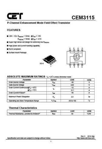
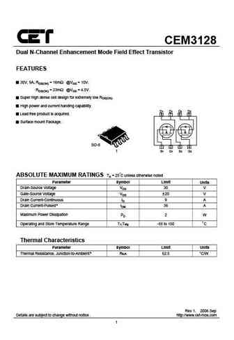
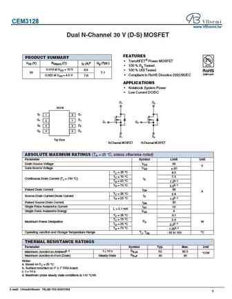
CEM3115 P-Channel Enhancement Mode Field Effect Transistor FEATURES -30V, -12A, RDS(ON) = 12m @VGS = -10V. RDS(ON) = 16m @VGS = -4.5V. Super high dense cell design for extremely low RDS(ON). High power and current handing capability. D D D D RoHS compliant. 8 7 6 5 Surface mount Package. SO-8 1 2 3 4 1 S S S G ABSOLUTE MAXIMUM RATINGS TA = 25 C unless otherwise noted Par
cem3138.pdf
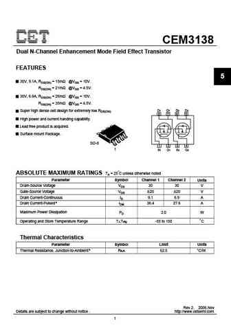
CEM3138 Dual N-Channel Enhancement Mode Field Effect Transistor FEATURES 5 30V, 9.1A, RDS(ON) = 15m @VGS = 10V. RDS(ON) = 21m @VGS = 4.5V. 30V, 6.9A, RDS(ON) = 26m @VGS = 10V. RDS(ON) = 35m @VGS = 4.5V. D1 D1 D2 D2 Super high dense cell design for extremely low RDS(ON). 8 7 6 5 High power and current handing capability. Lead free product is acquired. Surface mount Pac
cem3139.pdf
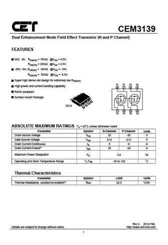
CEM3139 Dual Enhancement Mode Field Effect Transistor (N and P Channel) FEATURES 20V, 9A, RDS(ON) = 16m @VGS = 4.5V. RDS(ON) = 20m @VGS = 2.5V. -30V, -6A, RDS(ON) = 34m @VGS = -10V. RDS(ON) = 52m @VGS = -4.5V. Super high dense cell design for extremely low RDS(ON). D1 D1 D2 D2 High power and current handing capability. 8 7 6 5 RoHS compliant. Surface mount Package. S
cem3109.pdf
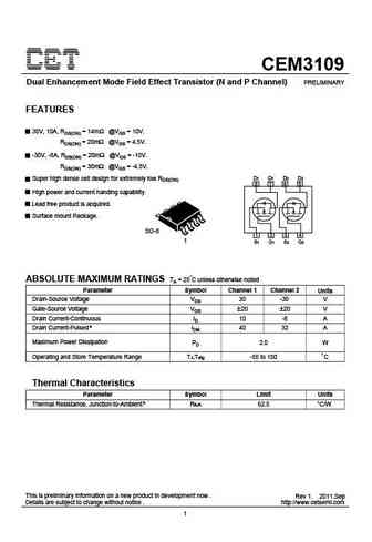
CEM3109 Dual Enhancement Mode Field Effect Transistor (N and P Channel) PRELIMINARY FEATURES 30V, 10A, RDS(ON) = 14m @VGS = 10V. RDS(ON) = 20m @VGS = 4.5V. -30V, -8A, RDS(ON) = 20m @VGS = -10V. RDS(ON) = 30m @VGS = -4.5V. D1 D1 D2 D2 Super high dense cell design for extremely low RDS(ON). 8 7 6 5 High power and current handing capability. Lead free product is acquired.
Otros transistores... BC2302T-2.8A, BC2302W, BC3134K, BC3134KT, CEB100N10L, CEC2533, CEC3257, CED3133, K3569
Parámetros del MOSFET. Cómo se afectan entre sí.
🌐 : EN ES РУ

Liste
Recientemente añadidas las descripciónes de los transistores:
MOSFET: CEM3139 | CEM3133 | CEM3115 | CED3133 | CEC3257 | CEC2533 | CEB100N10L | BC3134KT | BC3134K | BC2302W | BC2302T-2.8A | BC2302-2.8A | BC2301W | BC2301T-2.8A | CB3139KTB | CB2301DW
Popular searches
2n3904 equivalent | ksa1220 | s9015 | mje3055t datasheet | a733 | irf9630 | mj2955 | mje15030