IXTA15P15T Datasheet. Equivalente. Reemplazo. Hoja de especificaciones. Principales características
Número de Parte: IXTA15P15T
Tipo de FET: MOSFET
Polaridad de transistor: P
ESPECIFICACIONES MÁXIMAS
Pdⓘ - Máxima disipación de potencia: 150 W
|Vds|ⓘ - Voltaje máximo drenador-fuente: 150 V
|Vgs|ⓘ - Voltaje máximo fuente-puerta: 15 V
|Id|ⓘ - Corriente continua de drenaje: 15 A
Tjⓘ - Temperatura máxima de unión: 150 °C
CARACTERÍSTICAS ELÉCTRICAS
trⓘ - Tiempo de subida: 116 nS
RDSonⓘ - Resistencia estado encendido drenaje a fuente: 0.24 Ohm
Encapsulados: TO263
Búsqueda de reemplazo de IXTA15P15T MOSFET
- Selecciónⓘ de transistores por parámetros
IXTA15P15T datasheet
ixta152n085t ixtp152n085t.pdf
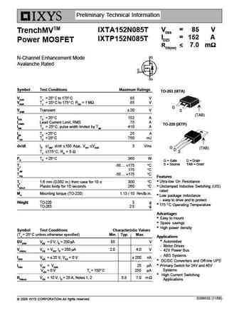
Preliminary Technical Information VDSS = 85 V IXTA152N085T TrenchMVTM ID25 = 152 A IXTP152N085T Power MOSFET RDS(on) 7.0 m N-Channel Enhancement Mode Avalanche Rated Symbol Test Conditions Maximum Ratings TO-263 (IXTA) VDSS TJ = 25 C to 175 C85 V VDGR TJ = 25 C to 175 C; RGS = 1 M 85 V G VGSM Transient 20 V S (TAB) ID25
ixta15n50l2.pdf
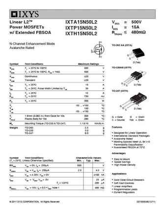
Linear L2TM VDSS = 500V IXTA15N50L2 Power MOSFETs ID25 = 15A IXTP15N50L2 RDS(on) 480m w/ Extended FBSOA IXTH15N50L2 N-Channel Enhancement Mode TO-263 AA (IXTA) Avalanche Rated G S D (Tab) Symbol Test Conditions Maximum Ratings TO-220AB (IXTP) VDSS TJ = 25 C to 150 C 500 V VDGR TJ = 25 C to 150 C, RGS = 1M 500 V VGSS Continuous 20 V
ixta152n085t7.pdf
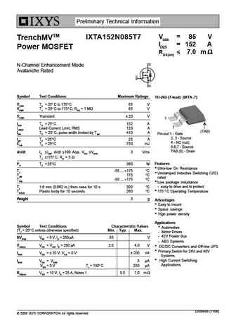
Preliminary Technical Information VDSS = 85 V IXTA152N085T7 TrenchMVTM ID25 = 152 A Power MOSFET RDS(on) 7.0 m N-Channel Enhancement Mode Avalanche Rated Symbol Test Conditions Maximum Ratings TO-263 (7-lead) (IXTA..7) VDSS TJ = 25 C to 175 C85 V VDGR TJ = 25 C to 175 C; RGS = 1 M 85 V VGSM Transient 20 V 1 ID25 TC = 25
ixta152n085t.pdf
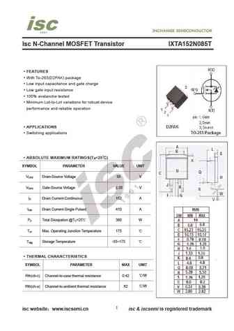
Isc N-Channel MOSFET Transistor IXTA152N085T FEATURES With To-263(D2PAK) package Low input capacitance and gate charge Low gate input resistance 100% avalanche tested Minimum Lot-to-Lot variations for robust device performance and reliable operation APPLICATIONS Switching applications ABSOLUTE MAXIMUM RATINGS(T =25 ) a SYMBOL PARAMETER VALUE UNIT V Drain-Source
Otros transistores... IXTA130N065T2, IXTA130N10T, IXTA130N10T7, IXTA140N055T2, IXTA140P05T, IXTA14N60P, IXTA152N085T, IXTA152N085T7, 4N60, IXTA160N04T2, IXTA160N075T, IXTA160N075T7, IXTA160N085T, IXTA160N10T, IXTA160N10T7, IXTA16N50P, IXTA170N075T2
🌐 : EN ES РУ

Liste
Recientemente añadidas las descripciónes de los transistores:
MOSFET: ASDM40N60KQ | ASDM40N40E | ASDM40N100P | ASDM40DN20E | ASDM3416EZA | ASDM3415ZA | ASDM3401ZA | ASDM3401 | ASDM3400ZA | ASDM30P30BE | RM50P30DF | CRTT095N12N | CRSS028N10N | CRST030N10N | CRJQ80N65F | ASDM20N20KQ
Popular searches
2sd424 | 2sc828 | 2n4125 | tip42c transistor | c1815 transistor datasheet | mj15003 | 2sa1015 | ksc3503