am3413p.pdf Principales características:
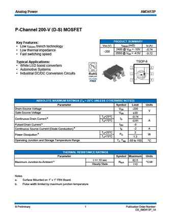
Analog Power AM3413P P-Channel 200-V (D-S) MOSFET PRODUCT SUMMARY Key Features rDS(on) (m ) VDS (V) ID (A) Low r trench technology DS(on) 2400 @ VGS = -10V -0.74 Low thermal impedance -200 2550 @ VGS = -4.5V -0.72 Fast switching speed TSOP-6 Typical Applications White LED boost converters Automotive Systems Industrial DC/DC Conversion Circuits ABSOLUTE MAXIMUM RATINGS (TA = 25 C UNLESS OTHERWISE NOTED) Parameter Symbol Limit Units Drain-Source Voltage VDS -200 V Gate-Source Voltage VGS 20 TA=25 C -0.74 ID Continuous Drain Current a TA=70 C A -0.61 Pulsed Drain Current b IDM -5 IS -2 A Continuous Source Current (Diode Conduction) a TA=25 C 2 PD W Power Dissipation a TA=70 C 1.3 Operating Junction and Storage Temperature Range TJ, Tstg -55 to 150 C THERMAL RESISTANCE RATINGS Parameter Symbol Maximum
Keywords - ALL TRANSISTORS. Principales características
am3413p.pdf Design, MOSFET, Power
am3413p.pdf RoHS Compliant, Service, Triacs, Semiconductor
am3413p.pdf Database, Innovation, IC, Electricity
Parámetros del transistor bipolar y su interrelación.
🌐 : EN ES РУ

Liste
Recientemente añadidas las descripciónes de los transistores:
BJT: ZDT6705 | GA1L4Z | GA1A4M | SBT42 | 2SA200-Y | 2SA200-O | 2SD882-Q | 2SD882-P | 2SD882-E | 2SC945-L | 2SC945-H | 2SC4226-R23 | 2SC3357-F | 2SC3357-E | 2SC3356-R26 | 2SC3356-R24 | 2SC3356-R23 | 2SB772-Q | 2SB772-P | 2SB772-E | 2SA1015-L
Popular searches
irfz44n | irf3205 | irfz44n datasheet | 2n4401 | bc547 transistor | bd139 | 2n4401 datasheet