j271.pdf Principales características:
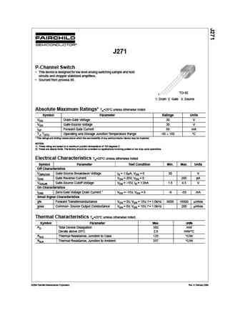
J271 P-Channel Switch This device is designed for low level analog switching sample and hold circuits and chopper stabilized amplifiers. Sourced from process 88. TO-92 1 1. Drain 2. Gate 3. Source Absolute Maximum Ratings* Ta=25 C unless otherwise noted Symbol Parameter Ratings Units VDG Drain-Gate Voltage 30 V VGS Gate-Source Voltage 30 V IGF Forward Gate Current 50 mA TJ, TSTG Operating and Storage Junction Temperature Range -55 150 C * This ratings are limiting values above which the serviceability of any semiconductor device may be impaired. NOTES 1) These rating are based on a maximum junction temperature of 150 degrees C. 2) These are steady limits. The factory should be consulted on applications involving pulsed or low duty cycle operations. Electrical Characteristics Ta=25 C unless otherwise noted Symbol Parameter Test Condition Min. Max. U
Keywords - ALL TRANSISTORS. Principales características
j271.pdf Design, MOSFET, Power
j271.pdf RoHS Compliant, Service, Triacs, Semiconductor
j271.pdf Database, Innovation, IC, Electricity
Parámetros del transistor bipolar y su interrelación.
🌐 : EN ES РУ

Liste
Recientemente añadidas las descripciónes de los transistores:
BJT: ZDT6705 | GA1L4Z | GA1A4M | SBT42 | 2SA200-Y | 2SA200-O | 2SD882-Q | 2SD882-P | 2SD882-E | 2SC945-L | 2SC945-H | 2SC4226-R23 | 2SC3357-F | 2SC3357-E | 2SC3356-R26 | 2SC3356-R24 | 2SC3356-R23 | 2SB772-Q | 2SB772-P | 2SB772-E | 2SA1015-L
Popular searches
irfz44n | irf3205 | irfz44n datasheet | 2n4401 | bc547 transistor | bd139 | 2n4401 datasheet