xp151a13comr.pdf Principales características:
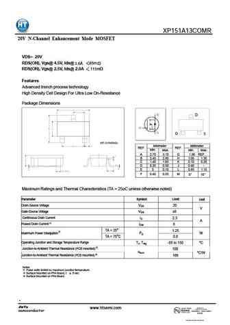
XP151A13COMR 20V N-Channel Enhancement Mode MOSFET VDS= 20V RDS(ON), Vgs@ 4.5V, Ids@ 3.6A 85m RDS(ON), Vgs@ 2.5V, Ids@ 2.0A 115m Features Advanced trench process technology High Density Cell Design For Ultra Low On-Resistance Package Dimensions D G S SOT-23(PACKAGE) Millimeter Millimeter REF. REF. Min. Max. Min. Max. A 2.70 3.10 G 1.90 REF. B 2.40 2.80 H 1.00 1.30 C 1.40 1.60 K 0.10 0.20 D 0.35 0.50 J 0.40 - E 0 0.10 L 0.85 1.15 F 0.45 0.55 M 0 10 Maximum Ratings and Thermal Characteristics (TA = 25oC unless otherwise noted) Parameter Symbol Limit Unit Drain-Source Voltage VDS 20 V Gate-Source Voltage VGS 8 Continuous Drain Current 2.3 ID A Pulsed Drain Current 1) IDM 8 TA = 25o 1.25 2) Maximum Power Dissipation PD W TA = 75oC 0.8 o Operating Junction and Storage Temperature Range TJ, Tstg -55 to 150 C Juncti... MOSTRAR MÁS ⇒
Keywords - ALL TRANSISTORS. Principales características
xp151a13comr.pdf Design, MOSFET, Power
xp151a13comr.pdf RoHS Compliant, Service, Triacs, Semiconductor
xp151a13comr.pdf Database, Innovation, IC, Electricity
Parámetros del transistor bipolar y su interrelación.
🌐 : EN ES РУ

Liste
Recientemente añadidas las descripciónes de los transistores:
BJT: ZDT6705 | GA1L4Z | GA1A4M | SBT42 | 2SA200-Y | 2SA200-O | 2SD882-Q | 2SD882-P | 2SD882-E | 2SC945-L | 2SC945-H | 2SC4226-R23 | 2SC3357-F | 2SC3357-E | 2SC3356-R26 | 2SC3356-R24 | 2SC3356-R23 | 2SB772-Q | 2SB772-P | 2SB772-E | 2SA1015-L
Popular searches
irfz44n | irf3205 | irfz44n datasheet | 2n4401 | bc547 transistor | bd139 | 2n4401 datasheet