ixta180n085t7.pdf Principales características:
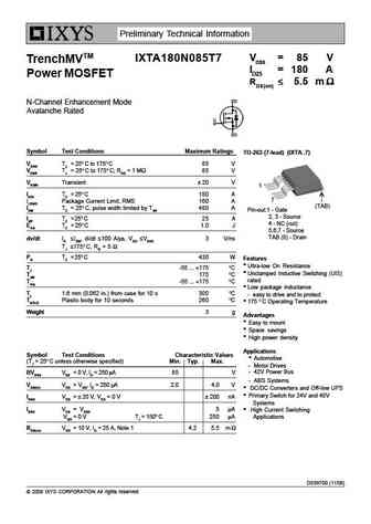
Preliminary Technical Information VDSS = 85 V IXTA180N085T7 TrenchMVTM ID25 = 180 A Power MOSFET RDS(on) 5.5 m N-Channel Enhancement Mode Avalanche Rated Symbol Test Conditions Maximum Ratings TO-263 (7-lead) (IXTA..7) VDSS TJ = 25 C to 175 C85 V VDGR TJ = 25 C to 175 C; RGS = 1 M 85 V VGSM Transient 20 V 1 ID25 TC = 25 C 180 A 7 ILRMS Package Current Limit, RMS 160 A (TAB) IDM TC = 25 C, pulse width limited by TJM 480 A Pin-out 1 - Gate 2, 3 - Source IAR TC = 25 C25 A 4 - NC (cut) EAS TC = 25 C 1.0 J 5,6,7 - Source TAB (8) - Drain dv/dt IS IDM, di/dt 100 A/ s, VDD VDSS 3 V/ns TJ 175 C, RG = 5 PD TC = 25 C 430 W Features Ultra-low On Resistance TJ -55 ... +175 C Unclamped Inductive Switching (UIS) TJM 175 C rated Tstg -55 ... +175 C Low package ind
Keywords - ALL TRANSISTORS. Principales características
ixta180n085t7.pdf Design, MOSFET, Power
ixta180n085t7.pdf RoHS Compliant, Service, Triacs, Semiconductor
ixta180n085t7.pdf Database, Innovation, IC, Electricity
Parámetros del transistor bipolar y su interrelación.
🌐 : EN ES РУ

Liste
Recientemente añadidas las descripciónes de los transistores:
BJT: ZDT6705 | GA1L4Z | GA1A4M | SBT42 | 2SA200-Y | 2SA200-O | 2SD882-Q | 2SD882-P | 2SD882-E | 2SC945-L | 2SC945-H | 2SC4226-R23 | 2SC3357-F | 2SC3357-E | 2SC3356-R26 | 2SC3356-R24 | 2SC3356-R23 | 2SB772-Q | 2SB772-P | 2SB772-E | 2SA1015-L
Popular searches
irfz44n | irf3205 | irfz44n datasheet | 2n4401 | bc547 transistor | bd139 | 2n4401 datasheet