kdb15n50.pdf Principales características:
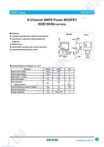
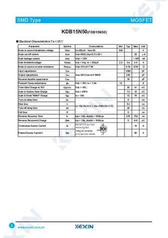
SMD Type MOSFET N-Channel SMPS Power MOSFET KDB15N50(FDB15N50) Features TO-263 Unit mm Low Gate Charge Qg results in Simple Drive Requirement +0.2 4.57-0.2 +0.1 Improved Gate, Avalanche and High Reapplied dv/dt 1.27-0.1 Ruggedness Reduced rDS(ON) Reduced Miller Capacitance and Low Input Capacitance +0.1 0.1max 1.27-0.1 Improved Switching Speed with Low EMI +0.1 0.81-0.1 2.54 1Gate +0.2 2Drain 2.54-0.2 +0.1 +0.2 5.08-0.1 0.4-0.2 3 Source Absolute Maximum Ratings Ta = 25 Parameter Symbol Rating Unit Drain to source voltage VDSS 500 V Gate to source voltage VGSS 30 V Drain current TC=25 ID 15 A Drain current-pulsed Idp 60 A Power dissipation 300 W PD Derate above 25 2 W/ Thermal Resistance Junction to Ambient R JA 62 /W Channel temperature Tch 175 Storage temperature Tstg -55to+175 1 www.kexin.com.cn +0.1 1.27 -0.1 5.60 +0.2 8.7 15.25 -0.
Keywords - ALL TRANSISTORS. Principales características
kdb15n50.pdf Design, MOSFET, Power
kdb15n50.pdf RoHS Compliant, Service, Triacs, Semiconductor
kdb15n50.pdf Database, Innovation, IC, Electricity
Parámetros del transistor bipolar y su interrelación.
🌐 : EN ES РУ

Liste
Recientemente añadidas las descripciónes de los transistores:
BJT: ZDT6705 | GA1L4Z | GA1A4M | SBT42 | 2SA200-Y | 2SA200-O | 2SD882-Q | 2SD882-P | 2SD882-E | 2SC945-L | 2SC945-H | 2SC4226-R23 | 2SC3357-F | 2SC3357-E | 2SC3356-R26 | 2SC3356-R24 | 2SC3356-R23 | 2SB772-Q | 2SB772-P | 2SB772-E | 2SA1015-L
Popular searches
irfz44n | irf3205 | irfz44n datasheet | 2n4401 | bc547 transistor | bd139 | 2n4401 datasheet