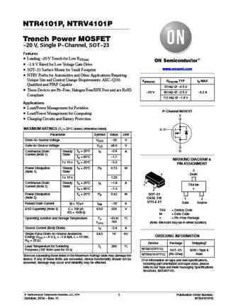
410 Equivalente. Reemplazo. Hoja de especificaciones. Principales características
Número de Parte: 410
Material: Si
Polaridad de transistor: NPN
ESPECIFICACIONES MÁXIMAS
Disipación total del dispositivo (Pc): 125 W
Tensión colector-base (Vcb): 200 V
Tensión colector-emisor (Vce): 200 V
Tensión emisor-base (Veb): 5 V
Corriente del colector DC máxima (Ic): 7 A
Temperatura operativa máxima (Tj): 150 °C
CARACTERÍSTICAS ELÉCTRICAS
Transición de frecuencia (ft): 4 MHz
Ganancia de corriente contínua (hfe): 10
Paquete / Cubierta: TO3
Búsqueda de reemplazo de 410
410 datasheet
aon7410.pdf
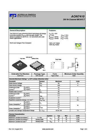
AON7410 30V N-Channel MOSFET General Description Features The AON7410 uses advanced trench technology and design VDS (V) = 30V to provide excellent RDS(ON) with low gate charge. This ID = 24A (VGS = 10V) device is suitable for use in DC - DC converters and Load RDS(ON)
ntmfs5c410nt3g.pdf
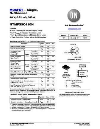
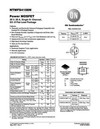
MOSFET Single, N-Channel 40 V, 0.92 mW, 300 A NTMFS5C410N Features www.onsemi.com Small Footprint (5x6 mm) for Compact Design Low RDS(on) to Minimize Conduction Losses Low QG and Capacitance to Minimize Driver Losses V(BR)DSS RDS(ON) MAX ID MAX These Devices are Pb-Free and are RoHS Compliant 40 V 0.92 mW @ 10 V 300 A MAXIMUM RATINGS (TJ = 25 C unless otherwise
me4410ad.pdf
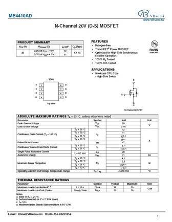
ME4410AD www.VBsemi.tw N-Channel 20V (D-S) MOSFET FEATURES PRODUCT SUMMARY Halogen-free VDS (V) RDS(on) ( ) ID (A)a Qg (Typ.) TrenchFET Power MOSFET 0.012 at VGS = 10 V 12 20 6.1 nC Optimized for High-Side Synchronous 0.015 at VGS = 4.5 V 11 Rectifier Operation 100 % Rg Tested 100 % UIS Tested APPLICATIONS Notebook CPU Core - High-Side Switch SO
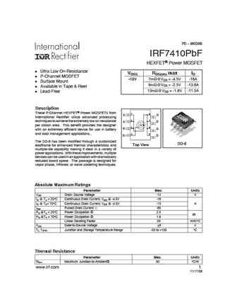
irfr410 irfu410.pdf
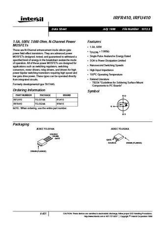
IRFR410, IRFU410 Data Sheet July 1999 File Number 3372.2 1.5A, 500V, 7.000 Ohm, N-Channel Power Features MOSFETs 1.5A, 500V These are N-Channel enhancement mode silicon gate rDS(ON) = 7.000 power field effect transistors. They are advanced power Single Pulse Avalanche Energy Rated MOSFETs designed, tested, and guaranteed to withstand a specified level of energy in the b
2sk2410.pdf
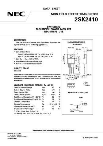
DATA SHEET MOS FIELD EFFECT TRANSISTOR 2SK2410 SWITCHING N-CHANNEL POWER MOS FET INDUSTRIAL USE DESCRIPTION PACKAGE DIMENSIONS The 2SK2410 is N-Channel MOS Field Effect Transistor de- (in millimeters) signed for high speed switching applications. 10.0 0.3 4.5 0.2 3.2 0.2 FEATURES 2.7 0.2 Low On-Resistance RDS(on)1 = 40 m MAX. (@ VGS = 10 V, ID = 15 A) RDS(on)2 =
me4410a.pdf
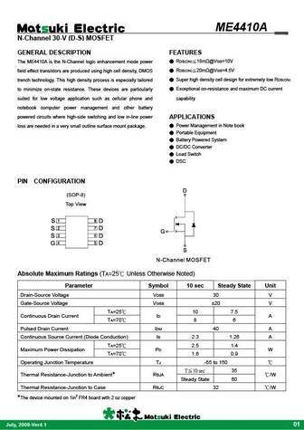
ME4410A N-Channel 30-V (D-S) MOSFET GENERAL DESCRIPTION FEATURES RDS(ON) 18m @VGS=10V The ME4410A is the N-Channel logic enhancement mode power RDS(ON) 20m @VGS=4.5V field effect transistors are produced using high cell density, DMOS Super high density cell design for extremely low RDS(ON) trench technology. This high density process is especially tailored
jsm7410.pdf
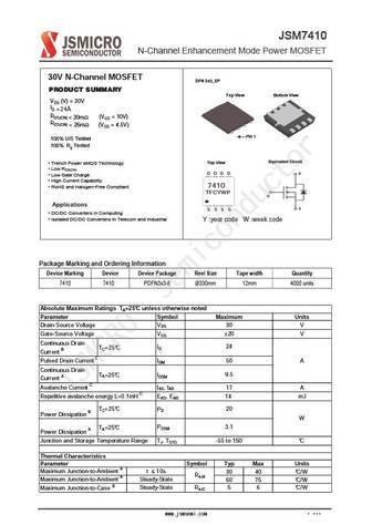
JSM7410 N-Channel Enhancement Mode Power MOSFET 30V N-Channel MOSFET DFN 3x3_EP PRODUCT SUMMARY Top View Bottom View VDS (V) = 30V ID =24A RDS(ON)
hy3410.pdf
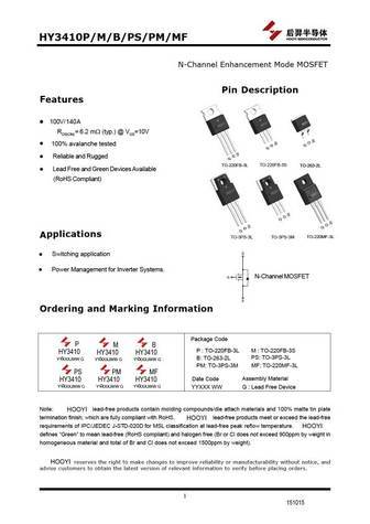
HY3410P/M/B/PS/PM/MF Absolute Maximum Ratings Symbol Parameter Rating Unit Common Ratings (TC=25 C Unless Otherwise Noted) VDSS Drain-Source Voltage 100 V VGSS Gate-Source Voltage 25 TJ Maximum Junction Temperature 175 C TSTG Storage Temperature Range -55 to 175 C IS Diode Continuous Forward Current TC=25 C 140 A Mounted on Large Heat Sink IDM Pulsed Drain Current *
vn2410l.rev1.pdf

MOTOROLA Order this document SEMICONDUCTOR TECHNICAL DATA by VN2410L/D TMOS FET Transistor VN2410L 3 DRAIN N Channel Enhancement 2 GATE 1 SOURCE MAXIMUM RATINGS Rating Symbol Value Unit 1 Drain Source Voltage VDSS 240 Vdc 2 3 Drain Gate Voltage VDGR 60 Vdc Gate Source Voltage CASE 29 04, STYLE 22 Continuous VGS 20 Vdc TO 92 (TO 226AA) Non rep
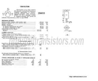
2n4410re.pdf
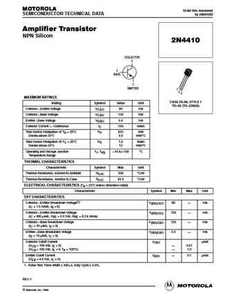
MOTOROLA Order this document SEMICONDUCTOR TECHNICAL DATA by 2N4410/D Amplifier Transistor NPN Silicon 2N4410 COLLECTOR 3 2 BASE 1 EMITTER 1 2 3 MAXIMUM RATINGS CASE 29 04, STYLE 1 Rating Symbol Value Unit TO 92 (TO 226AA) Collector Emitter Voltage VCEO 80 Vdc Collector Base Voltage VCBO 120 Vdc Emitter Base Voltage VEBO 5.0 Vdc Collector Current Continuou
mj410rev.pdf
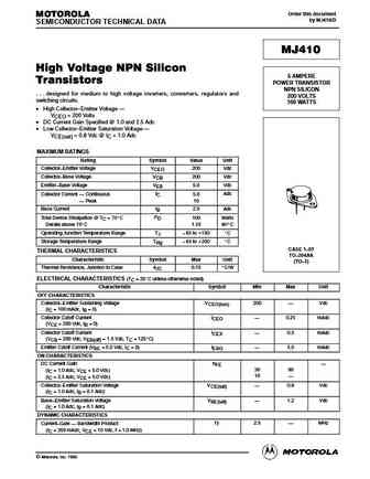
Order this document MOTOROLA by MJ410/D SEMICONDUCTOR TECHNICAL DATA MJ410 High Voltage NPN Silicon 5 AMPERE Transistors POWER TRANSISTOR NPN SILICON . . . designed for medium to high voltage inverters, converters, regulators and 200 VOLTS switching circuits. 100 WATTS High Collector Emitter Voltage VCEO = 200 Volts DC Current Gain Specified @ 1.0 and 2.5 Adc
vn2410l.pdf
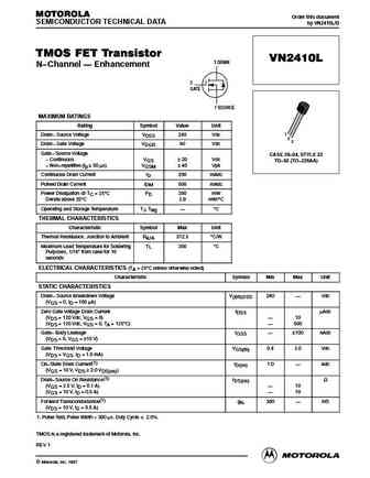
MOTOROLA Order this document SEMICONDUCTOR TECHNICAL DATA by VN2410L/D TMOS FET Transistor VN2410L 3 DRAIN N Channel Enhancement 2 GATE 1 SOURCE MAXIMUM RATINGS Rating Symbol Value Unit 1 Drain Source Voltage VDSS 240 Vdc 2 3 Drain Gate Voltage VDGR 60 Vdc Gate Source Voltage CASE 29 04, STYLE 22 Continuous VGS 20 Vdc TO 92 (TO 226AA) Non rep
mmjt9410.pdf
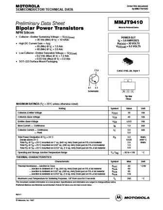
Order this document MOTOROLA by MMJT9410/D SEMICONDUCTOR TECHNICAL DATA MMJT9410 Preliminary Data Sheet Motorola Preferred Device Bipolar Power Transistors NPN Silicon Collector Emitter Sustaining Voltage VCEO(sus) POWER BJT = 30 Vdc (Min) @ IC = 10 mAdc IC = 3.0 AMPERES High DC Current Gain hFE BVCEO = 30 VOLTS = 85 (Min) @ IC = 1.0 Adc VCE(sat) = 0.2 VOLTS =
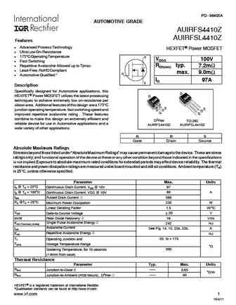
auirlr3410trl.pdf
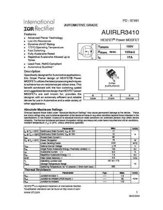
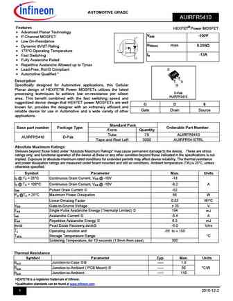
PD - 97491 AUTOMOTIVE GRADE AUIRLR3410 Features Advanced Planar Technology HEXFET Power MOSFET Low On-Resistance Dynamic dV/dT Rating D V(BR)DSS 100V 175 C Operating Temperature Fast Switching RDS(on) max. 105m G Fully Avalanche Rated Repetitive Avalanche Allowed up to ID 17A S Tjmax Lead-Free, RoHS Compliant Automotive Qualified * D Description Specifica
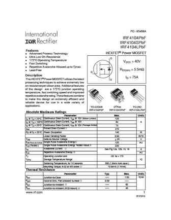
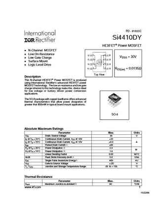
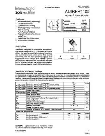
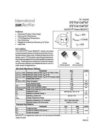
irf4104l.pdf
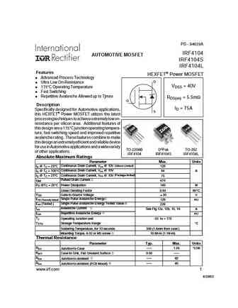
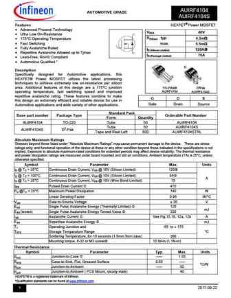
PD - 94639A IRF4104 AUTOMOTIVE MOSFET IRF4104S IRF4104L Features HEXFET Power MOSFET Advanced Process Technology D Ultra Low On-Resistance VDSS = 40V 175 C Operating Temperature Fast Switching Repetitive Avalanche Allowed up to Tjmax RDS(on) = 5.5m G Description ID = 75A Specifically designed for Automotive applications, S this HEXFET Power MOSFET
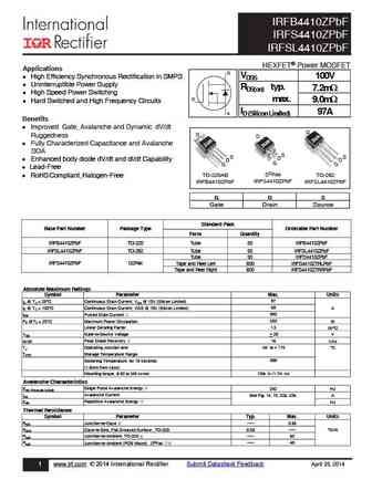
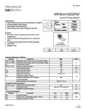
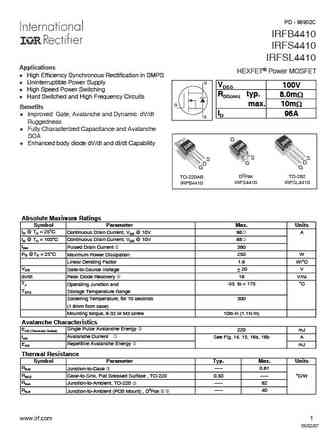
irfb4410pbf irfs4410pbf irfsl4410pbf.pdf
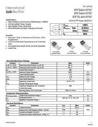
PD - 95707E IRFB4410PbF IRFS4410PbF IRFSL4410PbF Applications HEXFET Power MOSFET l High Efficiency Synchronous Rectification in SMPS l Uninterruptible Power Supply D VDSS 100V l High Speed Power Switching RDS(on) typ. 8.0m l Hard Switched and High Frequency Circuits G max. 10m ID S 88A Benefits l Improved Gate, Avalanche and Dynamic dV/dt Ruggedness l Fully Characterized
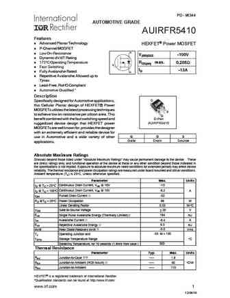
irfr4105zpbf irfu4105zpbf.pdf
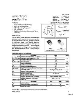
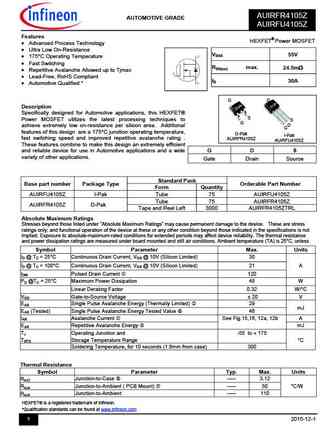
PD - 95374B IRFR4105ZPbF IRFU4105ZPbF Features HEXFET Power MOSFET Advanced Process Technology D Ultra Low On-Resistance VDSS = 55V 175 C Operating Temperature Fast Switching RDS(on) = 24.5m Repetitive Avalanche Allowed up to Tjmax G Lead-Free ID = 30A Description S This HEXFET Power MOSFET utilizes the latest processing techniques to achieve extremely low on-re
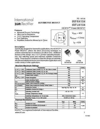
auirfr4104tr.pdf
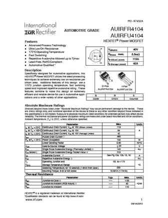
PD - 97452A AUIRFR4104 AUTOMOTIVE GRADE AUIRFU4104 HEXFET Power MOSFET Features Advanced Process Technology D Ultra Low On-Resistance V(BR)DSS 40V 175 C Operating Temperature RDS(on) max. 5.5m Fast Switching G Repetitive Avalanche Allowed up to Tjmax ID (Silicon Limited) 119A Lead-Free, RoHS Compliant S ID (Package Limited) 42A Automotive Q
auirfb4410.pdf
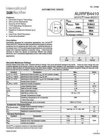
PD - 97598 AUTOMOTIVE GRADE AUIRFB4410 HEXFET Power MOSFET Features Advanced Process Technology D VDSS 100V Ultra Low On-Resistance Dynamic dV/dT Rating RDS(on) typ. 8.0m 175 C Operating Temperature max. 10m Fast Switching G Repetitive Avalanche Allowed up to ID (Silicon Limited) 88A Tjmax Lead-Free, RoHS Compliant ID (Package Limited)
irfp2410.pdf
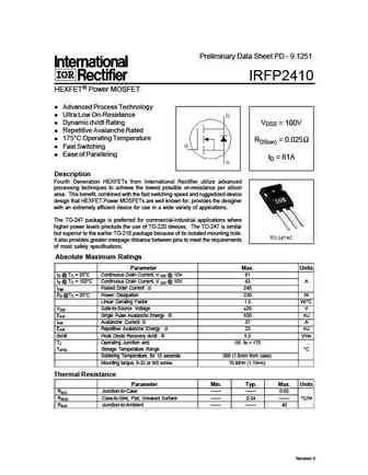
Preliminary Data Sheet PD - 9.1251 IRFP2410 HEXFET Power MOSFET Advanced Process Technology Ultra Low On-Resistance Dynamic dv/dt Rating VDSS = 100V Repetitive Avalanche Rated 175 C Operating Temperature RDS(on) = 0.025 Fast Switching Ease of Paralleling ID = 61A Description Fourth Generation HEXFETs from International Rectifier utilize advanced processing techniques to achi
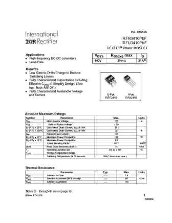
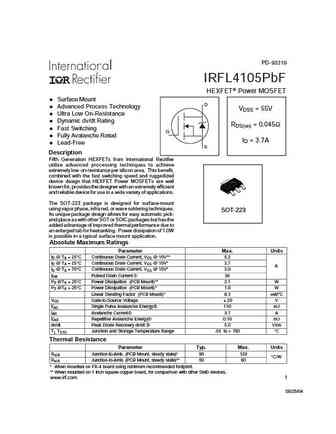
irfr3410.pdf
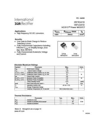
PD - 94505 IRFR3410 IRFU3410 HEXFET Power MOSFET Applications VDSS RDS(on) max ID l High frequency DC-DC converters 100V 39m 31A Benefits l Low Gate-to-Drain Charge to Reduce Switching Losses l Fully Characterized Capacitance Including Effective COSS to Simplify Design, (See App. Note AN1001) l Fully Characterized Avalanche Voltage D-Pak I-Pak and Current IRFR3410 IRFU
irfi4410zpbf.pdf
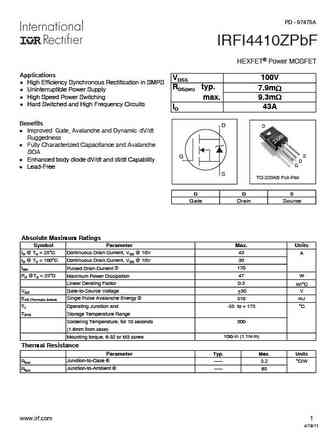
PD - 97475A IRFI4410ZPbF HEXFET Power MOSFET Applications VDSS 100V l High Efficiency Synchronous Rectification in SMPS RDS(on) typ. 7.9m l Uninterruptible Power Supply l High Speed Power Switching max. 9.3m l Hard Switched and High Frequency Circuits ID 43A Benefits D D l Improved Gate, Avalanche and Dynamic dV/dt Ruggedness l Fully Characterized Capacitance and Avala
irf9410.pdf
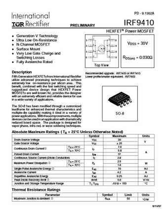
PD - 9.1562A IRF9410 PRELIMINARY HEXFET Power MOSFET Generation V Technology A A 1 8 S D Ultra Low On-Resistance VDSS = 30V 2 7 N-Channel MOSFET S D Surface Mount 3 6 S D Very Low Gate Charge and 4 5 G D Switching Losses RDS(on) = 0.030 Fully Avalanche Rated Top View Description Recommended upgrade IRF7403 or IRF7413 Fifth Generation HEXFETs from Internationa
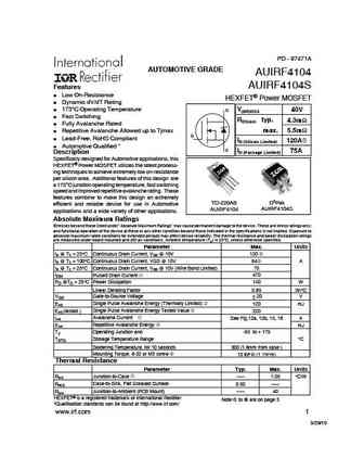
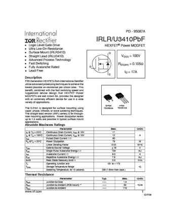
irlr3410pbf irlu3410pbf.pdf

PD - 95087A IRLR/U3410PbF l Logic Level Gate Drive HEXFET Power MOSFET l Ultra Low On-Resistance l Surface Mount (IRLR3410) D l Straight Lead (IRLU3410) VDSS = 100V l Advanced Process Technology l Fast Switching RDS(on) = 0.105 G l Fully Avalanche Rated l Lead-Free ID = 17A S Description Fifth Generation HEXFETs from International Rectifier utilize advanced processing tec
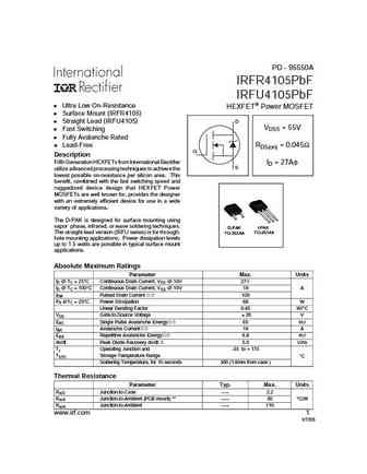
irfr5410pbf irfu5410pbf.pdf

PD -95314A IRFR5410PbF IRFU5410PbF HEXFET Power MOSFET l Ultra Low On-Resistance l P-Channel D VDSS = -100V l Surface Mount (IRFR5410) l Straight Lead (IRFU5410) l Advanced Process Technology RDS(on) = 0.205 G l Fast Switching l Fully Avalanche Rated ID = -13A S l Lead-Free Description Fifth Generation HEXFETs from International Rectifier utilize advanced processing tech
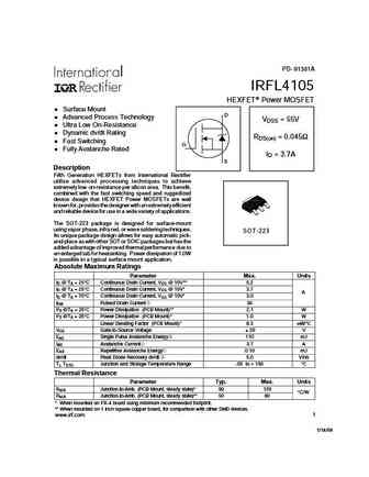
irf7410pbf-1.pdf
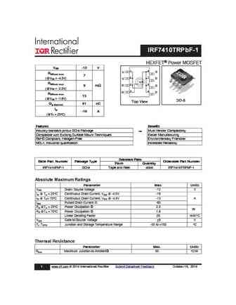
IRF7410TRPbF-1 HEXFET Power MOSFET VDS -12 V A 1 8 S D RDS(on) max 7 2 7 (@V = -4.5V) D GS S RDS(on) max 3 6 S 9 m D (@V = -2.5V) GS 4 5 G D RDS(on) max 13 (@V = -1.8V) GS SO-8 Top View Qg (typical) 91 nC ID -16 A (@T = 25 C) A Features Benefits Industry-standard pinout SO-8 Package Multi-Vendor Compatibility Compatible with Existing Surface Mount T
irf4104lpbf irf4104pbf irf4104spbf.pdf

PD - 95468A IRF4104PbF IRF4104SPbF IRF4104LPbF Features HEXFET Power MOSFET Advanced Process Technology Ultra Low On-Resistance D 175 C Operating Temperature VDSS = 40V Fast Switching Repetitive Avalanche Allowed up to Tjmax RDS(on) = 5.5m Lead-Free G Description ID = 75A This HEXFET Power MOSFET utilizes the latest S processing techniques to achieve extremely
auirfs4410z auirfsl4410z.pdf
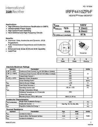
PD - 96405A AUTOMOTIVE GRADE AUIRFS4410Z AUIRFSL4410Z Features l Advanced Process Technology HEXFET Power MOSFET l Ultra Low On-Resistance l 175 C Operating Temperature D VDSS 100V l Fast Switching l Repetitive Avalanche Allowed up to Tjmax RDS(on) typ. 7.2m l Lead-Free, RoHS Compliant max. 9.0m G l Automotive Qualified * ID 97A S Description Specifically desig
irf4104pbf irf4104spbf irf4104lpbf.pdf
PD - 95468A IRF4104PbF IRF4104SPbF IRF4104LPbF Features HEXFET Power MOSFET Advanced Process Technology Ultra Low On-Resistance D 175 C Operating Temperature VDSS = 40V Fast Switching Repetitive Avalanche Allowed up to Tjmax RDS(on) = 5.5m Lead-Free G Description ID = 75A This HEXFET Power MOSFET utilizes the latest S processing techniques to achieve extremely
irf7410gpbf.pdf
PD - 96247 IRF7410GPbF HEXFET Power MOSFET l Ultra Low On-Resistance VDSS RDS(on) max ID l P-Channel MOSFET -12V 7m @VGS = -4.5V -16A l Surface Mount 9m @VGS = -2.5V -13.6A l Available in Tape & Reel 13m @VGS = -1.8V -11.5A l Lead-Free l Halogen-Free Description A These P-Channel HEXFET Power MOSFETs from 1 8 S D International Rectifier utilize advanced processing
irfb4410zpbf irfs4410zpbf irfsl4410zpbf.pdf
IRFB4410ZPbF IRFS4410ZPbF IRFSL4410ZPbF HEXFET Power MOSFET Applications D VDSS l High Efficiency Synchronous Rectification in SMPS 100V l Uninterruptible Power Supply RDS(on) typ. 7.2m l High Speed Power Switching G max. 9.0m l Hard Switched and High Frequency Circuits ID (Silicon Limited) 97A S Benefits l Improved Gate, Avalanche and Dynamic dV/dt D D Ruggedness D l
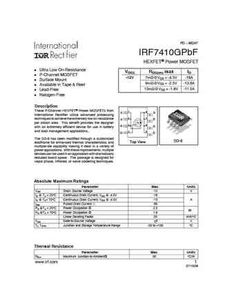
irf7410.pdf
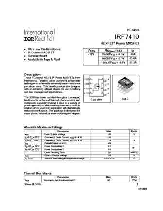
PD - 94025 IRF7410 HEXFET Power MOSFET Ultra Low On-Resistance VDSS RDS(on) max ID P-Channel MOSFET -12V 7m @VGS = -4.5V -16A Surface Mount 9m @VGS = -2.5V -13.6A Available in Tape & Reel 13m @VGS = -1.8V -11.5A Description A These P-Channel HEXFET Power MOSFETs from 1 8 S D International Rectifier utilize advanced processing 2 7 techniques to achieve the extrem
si4410dy.pdf
PD - 91853C Si4410DY HEXFET Power MOSFET N-Channel MOSFET A A Low On-Resistance 1 8 S D VDSS = 30V Low Gate Charge 2 7 S D Surface Mount 3 6 S D Logic Level Drive 4 5 G D RDS(on) = 0.0135 Top View Description This N-channel HEXFET Power MOSFET is produced using International Rectifier's advanced HEXFET power MOSFET technology. The low on-resistance and low gat
auirf4104strl.pdf
PD - 97471A AUTOMOTIVE GRADE AUIRF4104 AUIRF4104S Features Low On-Resistance HEXFET Power MOSFET Dynamic dV/dT Rating 175 C Operating Temperature D V(BR)DSS 40V Fast Switching RDS(on) typ. 4.3m Fully Avalanche Rated Repetitive Avalanche Allowed up to Tjmax max. 5.5m G Lead-Free, RoHS Compliant ID (Silicon Limited) 120A Automotive Qualified * S ID (Package Li
irlr3410.pdf
PD - 91607B IRLR/U3410 HEXFET Power MOSFET Logic Level Gate Drive D Ultra Low On-Resistance VDSS = 100V Surface Mount (IRLR3410) Straight Lead (IRLU3410) RDS(on) = 0.105 Advanced Process Technology G Fast Switching ID = 17A Fully Avalanche Rated S Description Fifth Generation HEXFETs from International Rectifier utilize advanced processing techniques to achieve the
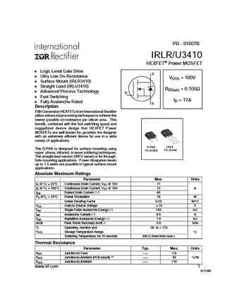
irfl4105.pdf
PD- 91381A IRFL4105 HEXFET Power MOSFET Surface Mount D Advanced Process Technology VDSS = 55V Ultra Low On-Resistance Dynamic dv/dt Rating RDS(on) = 0.045 Fast Switching G Fully Avalanche Rated ID = 3.7A S Description Fifth Generation HEXFETs from International Rectifier utilize advanced processing techniques to achieve extremely low on-resistance per silicon area.
irf9410pbf.pdf
PD - 95260 IRF9410PbF HEXFET Power MOSFET l Generation V Technology A l Ultra Low On-Resistance A 1 8 S D l N-Channel MOSFET VDSS = 30V 2 7 l Surface Mount S D l Very Low Gate Charge and 3 6 S D Switching Losses 4 5 G D RDS(on) = 0.030 l Fully Avalanche Rated l Lead-Free Top View Description Recommended upgrade IRF7403 or IRF7413 Fifth Generation HEXFETs from Int
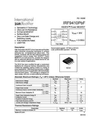
auirfr4105ztr.pdf
PD - 97544 AUTOMOTIVE GRADE AUIRFR4105Z AUIRFU4105Z HEXFET Power MOSFET Features D Advanced Process Technology V(BR)DSS 55V Ultra Low On-Resistance 175 C Operating Temperature RDS(on) max. 24.5m G Fast Switching Repetitive Avalanche Allowed up to Tjmax ID S 30A Lead-Free, RoHS Compliant Automotive Qualified * Description D Specifically de
irfr4105.pdf
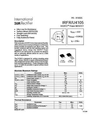
PD - 91302C IRFR/U4105 HEXFET Power MOSFET Ultra Low On-Resistance D Surface Mount (IRFR4105) VDSS = 55V Straight Lead (IRFU4105) Fast Switching RDS(on) = 0.045 Fully Avalanche Rated G Description ID = 27A S Fifth Generation HEXFETs from International Rectifier utilize advanced processing techniques to achieve the lowest possible on-resistance per silicon area. This
irfb4410.pdf

PD - 96902C IRFB4410 IRFS4410 IRFSL4410 Applications HEXFET Power MOSFET l High Efficiency Synchronous Rectification in SMPS l Uninterruptible Power Supply D VDSS 100V l High Speed Power Switching RDS(on) typ. 8.0m l Hard Switched and High Frequency Circuits G max. 10m Benefits ID 96A l Improved Gate, Avalanche and Dynamic dV/dt S Ruggedness l Fully Characterized Capacita
irfi4410zgpbf.pdf
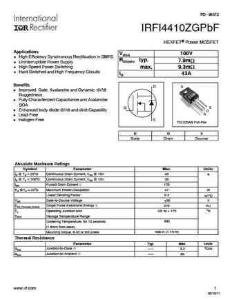
PD - 96372 IRFI4410ZGPbF HEXFET Power MOSFET Applications VDSS 100V l High Efficiency Synchronous Rectification in SMPS RDS(on) typ. 7.9m l Uninterruptible Power Supply l High Speed Power Switching max. 9.3m l Hard Switched and High Frequency Circuits ID 43A Benefits D D l Improved Gate, Avalanche and Dynamic dV/dt Ruggedness l Fully Characterized Capacitance and Avalanche
auirfr4105tr.pdf
PD - 97597A AUTOMOTIVE GRADE AUIRFR4105 HEXFET Power MOSFET Features D V(BR)DSS 55V Advanced Planar Technology Low On-Resistance RDS(on) max. 45m Dynamic dV/dT Rating G ID (Silicon Limited) 27A 175 C Operating Temperature Fast Switching ID (Package Limited) 20A S Fully Avalanche Rated Repetitive Avalanche Allowed up toTjmax Lead-Free,
irfr5410.pdf
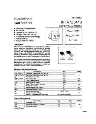
PD - 9.1533A IRFR/U5410 HEXFET Power MOSFET l Ultra Low On-Resistance D l P-Channel VDSS = -100V l Surface Mount (IRFR5410) l Straight Lead (IRFU5410) RDS(on) = 0.205W l Advanced Process Technology G l Fast Switching ID = -13A l Fully Avalanche Rated S Description Fifth Generation HEXFETs from International Rectifier utilize advanced processing techniques to achieve extreme
irfu4104.pdf
PD - 94728 IRFR4104 AUTOMOTIVE MOSFET IRFU4104 HEXFET Power MOSFET Features D Advanced Process Technology VDSS = 40V Ultra Low On-Resistance 175 C Operating Temperature RDS(on) = 5.5m Fast Switching G Repetitive Avalanche Allowed up to Tjmax ID = 42A S Description Specifically designed for Automotive applications, this HEXFET Power MOSFET utilizes
irfr4104pbf irfu4104pbf.pdf
PD - 95425B IRFR4104PbF IRFU4104PbF HEXFET Power MOSFET Features D l Advanced Process Technology VDSS = 40V l Ultra Low On-Resistance l 175 C Operating Temperature RDS(on) = 5.5m l Fast Switching G l Repetitive Avalanche Allowed up to Tjmax l Lead-Free ID = 42A S Description This HEXFET Power MOSFET utilizes the latest processing techniques to achieve extremely low on
irfr3410pbf irfu3410pbf.pdf
PD - 95514A IRFR3410PbF IRFU3410PbF HEXFET Power MOSFET Applications VDSS RDS(on) max ID l High frequency DC-DC converters 100V 39m 31A l Lead-Free Benefits l Low Gate-to-Drain Charge to Reduce Switching Losses l Fully Characterized Capacitance Including Effective COSS to Simplify Design, (See App. Note AN1001) l Fully Characterized Avalanche Voltage D-Pak I-Pak and Cu
irf7410pbf.pdf
PD - 96028B IRF7410PbF HEXFET Power MOSFET l Ultra Low On-Resistance VDSS RDS(on) max ID l P-Channel MOSFET -12V 7m @VGS = -4.5V -16A l Surface Mount 9m @VGS = -2.5V -13.6A l Available in Tape & Reel 13m @VGS = -1.8V -11.5A l Lead-Free Description A These P-Channel HEXFET Power MOSFETs from 1 8 S D International Rectifier utilize advanced processing 2 7 techniques
irfp4410zpbf.pdf
PD - 97309A IRFP4410ZPbF HEXFET Power MOSFET Applications VDSS 100V l High Efficiency Synchronous Rectification in SMPS RDS(on) typ. l Uninterruptible Power Supply 7.2m l High Speed Power Switching max. 9.0m l Hard Switched and High Frequency Circuits ID (Silicon Limited) 97A Benefits l Improved Gate, Avalanche and Dynamic dV/dt D D Ruggedness l Fully Characterized Cap
irlu3410pbf irlr3410pbf.pdf
PD - 95087A IRLR/U3410PbF l Logic Level Gate Drive HEXFET Power MOSFET l Ultra Low On-Resistance l Surface Mount (IRLR3410) D l Straight Lead (IRLU3410) VDSS = 100V l Advanced Process Technology l Fast Switching RDS(on) = 0.105 G l Fully Avalanche Rated l Lead-Free ID = 17A S Description Fifth Generation HEXFETs from International Rectifier utilize advanced processing tec
irfr4105pbf irfu4105pbf.pdf
PD - 95550A IRFR4105PbF IRFU4105PbF l Ultra Low On-Resistance HEXFET Power MOSFET l Surface Mount (IRFR4105) l Straight Lead (IRFU4105) D VDSS = 55V l Fast Switching l Fully Avalanche Rated l Lead-Free RDS(on) = 0.045 G Description Fifth Generation HEXFETs from International Rectifier ID = 27A S utilize advanced processing techniques to achieve the lowest possible on-r
irfs4410pbf irfsl4410pbf.pdf

PD - 95707E IRFB4410PbF IRFS4410PbF IRFSL4410PbF Applications HEXFET Power MOSFET l High Efficiency Synchronous Rectification in SMPS l Uninterruptible Power Supply D VDSS 100V l High Speed Power Switching RDS(on) typ. 8.0m l Hard Switched and High Frequency Circuits G max. 10m ID S 88A Benefits l Improved Gate, Avalanche and Dynamic dV/dt Ruggedness l Fully Characterized
irfb4410zgpbf.pdf
PD - 96213 IRFB4410ZGPbF HEXFET Power MOSFET D Applications VDSS 100V l High Efficiency Synchronous Rectification in SMPS RDS(on) typ. l Uninterruptible Power Supply 7.2m l High Speed Power Switching G max. 9.0m l Hard Switched and High Frequency Circuits ID (Silicon Limited) 97A S Benefits D l Improved Gate, Avalanche and Dynamic dV/dt Ruggedness l Fully Characterized C
irfl4105pbf.pdf
PD- 95319 IRFL4105PbF HEXFET Power MOSFET Surface Mount D Advanced Process Technology VDSS = 55V Ultra Low On-Resistance Dynamic dv/dt Rating RDS(on) = 0.045 Fast Switching G Fully Avalanche Rated ID = 3.7A Lead-Free S Description Fifth Generation HEXFETs from International Rectifier utilize advanced processing techniques to achieve extremely low on-resistance per
irfb4410 irfs4410 irfsl4410.pdf
PD - 96902C IRFB4410 IRFS4410 IRFSL4410 Applications HEXFET Power MOSFET l High Efficiency Synchronous Rectification in SMPS l Uninterruptible Power Supply D VDSS 100V l High Speed Power Switching RDS(on) typ. 8.0m l Hard Switched and High Frequency Circuits G max. 10m Benefits ID 96A l Improved Gate, Avalanche and Dynamic dV/dt S Ruggedness l Fully Characterized Capacita
bf410a 410b 410c 410d.pdf
DISCRETE SEMICONDUCTORS DATA SHEET BF410A to D N-channel silicon field-effect transistors December 1990 Product specification File under Discrete Semiconductors, SC07 Philips Semiconductors Product specification N-channel silicon field-effect transistors BF410A to D DESCRIPTION PINNING - TO-92 VARIANT Asymmetrical N-channel planar 1 = drain epitaxial junction field-effect 2 = sou
bfg410w.pdf
DISCRETE SEMICONDUCTORS DATA SHEET BFG410W NPN 22 GHz wideband transistor Product specification 1998 Mar 11 Supersedes data of 1997 Oct 29 NXP Semiconductors Product specification NPN 22 GHz wideband transistor BFG410W FEATURES PINNING Very high power gain PIN DESCRIPTION Low noise figure 1emitter High transition frequency 2 base Emitter is thermal lead 3emitt
pbss9410pa.pdf
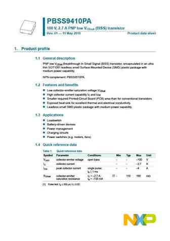
PBSS9410PA 100 V, 2.7 A PNP low VCEsat (BISS) transistor Rev. 01 11 May 2010 Product data sheet 1. Product profile 1.1 General description PNP low VCEsat Breakthrough In Small Signal (BISS) transistor, encapsulated in an ultra thin SOT1061 leadless small Surface-Mounted Device (SMD) plastic package with medium power capability. NPN complement PBSS8510PA. 1.2 Features and benefit
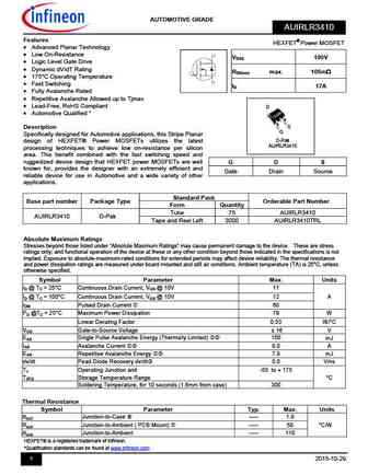
sd4100.pdf
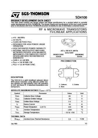
SD4100 PRODUCT DEVELOPMENT DATA SHEET This data sheet contains the design criteria and target specifications for a product which is currently under development by SGS-THOMSON. The design criteria and specifications of this item could change prior to introduction and SGS-THOMSON assumes no liability for use of information contained herein. RF & MICROWAVE TRANSISTORS TV/LINEAR APPLICATIONS
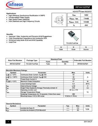
buf410a.pdf
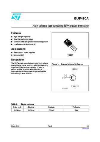
BUF410A High voltage fast-switching NPN power transistor Features High voltage capability Very high switching speed Minimum lot-to-lot spread for reliable operation Low base-drive requirements Applications 3 2 1 Switch mode power supplies TO-247 Motor control Description The BUF410A is manufactured using high voltage Figure 1. Internal schematic diagram
buf410.pdf
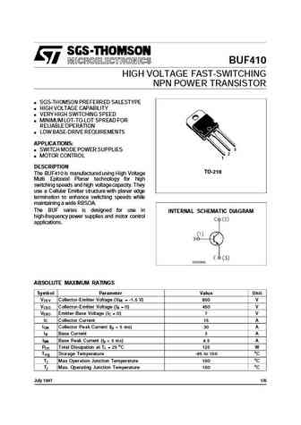
BUF410 HIGH VOLTAGE FAST-SWITCHING NPN POWER TRANSISTOR SGS-THOMSON PREFERRED SALESTYPE HIGH VOLTAGE CAPABILITY VERY HIGH SWITCHING SPEED MINIMUM LOT-TO-LOT SPREAD FOR RELIABLE OPERATION LOW BASE-DRIVE REQUIREMENTS APPLICATIONS 3 SWITCH MODE POWER SUPPLIES 2 MOTOR CONTROL 1 DESCRIPTION TO-218 The BUF410 is manufactured using High Voltage Multi Epitaxial Planar technolo
sth410n4f7-2ag sth410n4f7-6ag.pdf
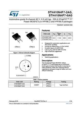
STH410N4F7-2AG, STH410N4F7-6AG Automotive-grade N-channel 40 V, 0.8 m typ., 200 A STripFET F7 Power MOSFETs in H PAK-2 and H PAK-6 packages Datasheet - production data Features R DS(on) Order code VDS ID PTOT max. STH410N4F7-2AG 40 V 1.1 m 200 A 365 W STH410N4F7-6AG Designed for automotive applications and AEC-Q101 qualified Among the lowest RDS(on)
rn1410 rn1411.pdf
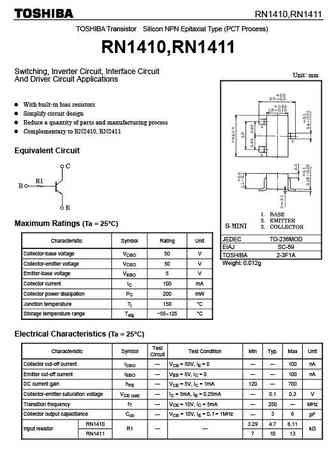
RN1410,RN1411 TOSHIBA Transistor Silicon NPN Epitaxial Type (PCT Process) RN1410,RN1411 Switching, Inverter Circuit, Interface Circuit Unit mm And Driver Circuit Applications With built-in bias resistors Simplify circuit design Reduce a quantity of parts and manufacturing process Complementary to RN2410, RN2411 Equivalent Circuit Maximum Ratings (Ta = 25 C) JED
mp4104.pdf
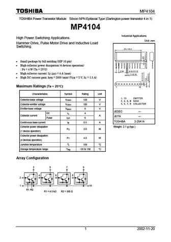
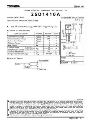
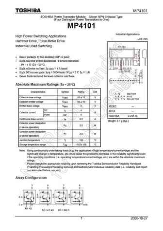
MP4104 TOSHIBA Power Transistor Module Silicon NPN Epitaxial Type (Darlington power transistor 4 in 1) MP4104 Industrial Applications High Power Switching Applications. Unit mm Hammer Drive, Pulse Motor Drive and Inductive Load Switching. Small package by full molding (SIP 10 pin) High collector power dissipation (4 devices operation) P = 4 W (Ta = 25 C) T
ssm6j410tu.pdf
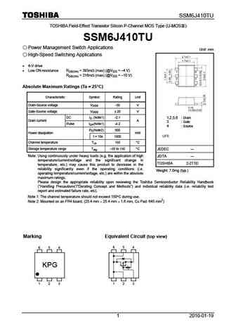
SSM6J410TU TOSHIBA Field-Effect Transistor Silicon P-Channel MOS Type (U-MOS ) SSM6J410TU Power Management Switch Applications Unit mm High-Speed Switching Applications 4-V drive Low ON-resistance RDS(ON) = 393m (max) (@VGS = 4 V) RDS(ON) = 216m (max) (@VGS = 10 V) Absolute Maximum Ratings (Ta = 25 C) Characteristic Symbol Rating Unit Drain-Sou
mp4410 .pdf
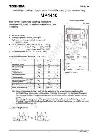
MP4410 TOSHIBA Power MOS FET Module Silicon N Channel MOS Type (Four L2- -MOSV in One) MP4410 Industrial Applications High Power, High Speed Switching Applications Unit mm Hammer Drive, Pulse Motor Drive and Inductive Load Switching 4-V gate drivability Small package by full molding (SIP 12 pin) High drain power dissipation (4-device operation) PT = 28 W (T
2sk4104.pdf
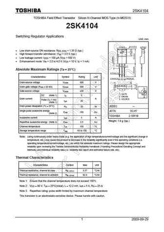
2SK4104 TOSHIBA Field Effect Transistor Silicon N Channel MOS Type ( -MOSVI) 2SK4104 Switching Regulator Applications Unit mm Low drain-source ON resistance RDS (ON) = 1.35 (typ.) High forward transfer admittance Yfs = 3.5 S (typ.) Low leakage current IDSS = 100 A (VDS = 500 V) Enhancement mode Vth = 2.0 to 4.0 V (VDS = 10 V, ID = 1 mA) Absolute M
rn2410-rn2411.pdf
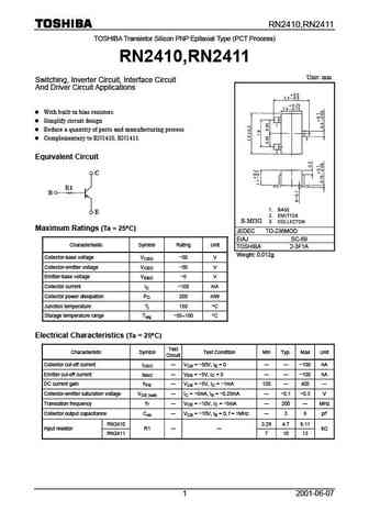
RN2410,RN2411 TOSHIBA Transistor Silicon PNP Epitaxial Type (PCT Process) RN2410,RN2411 Unit mm Switching, Inverter Circuit, Interface Circuit And Driver Circuit Applications With built-in bias resistors Simplify circuit design Reduce a quantity of parts and manufacturing process Complementary to RN1410, RN1411 Equivalent Circuit Maximum Ratings (Ta = 25 C)
2sk4106.pdf

2SK4106 TOSHIBA Field Effect Transistor Silicon N Channel MOS Type ( -MOSVI) 2SK4106 Switching Regulator Applications Unit mm Low drain-source ON resistance RDS (ON) = 0.4 (typ.) High forward transfer admittance Yfs = 8.5 S (typ.) Low leakage current IDSS = 100 A (max) (VDS = 500 V) Enhancement mode Vth = 2.0 to 4.0 V (VDS = 10 V, ID = 1 mA) Absol
2sk4105.pdf
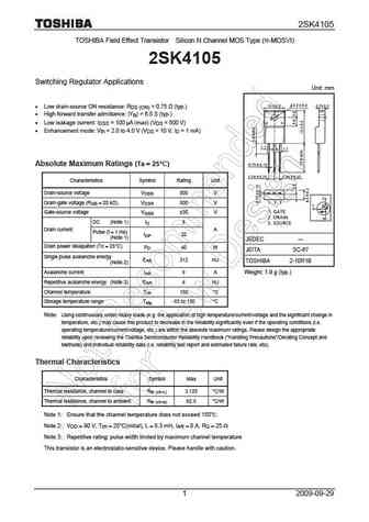
2SK4105 TOSHIBA Field Effect Transistor Silicon N Channel MOS Type ( -MOSVI) 2SK4105 Switching Regulator Applications Unit mm Low drain-source ON resistance RDS (ON) = 0.75 (typ.) High forward transfer admittance Yfs = 6.5 S (typ.) Low leakage current IDSS = 100 A (max) (VDS = 500 V) Enhancement mode Vth = 2.0 to 4.0 V (VDS = 10 V, ID = 1 mA) Abso
mp4410.pdf
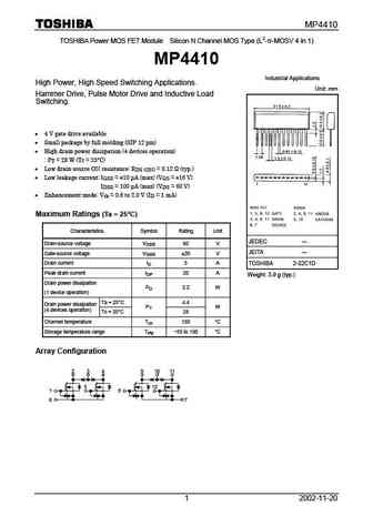
MP4410 TOSHIBA Power MOS FET Module Silicon N Channel MOS Type (L2- -MOSV 4 in 1) MP4410 Industrial Applications High Power, High Speed Switching Applications. Unit mm Hammer Drive, Pulse Motor Drive and Inductive Load Switching. 4 V gate drive available Small package by full molding (SIP 12 pin) High drain power dissipation (4 devices operation) PT = 28 W
mp4104 .pdf

MP4104 TOSHIBA Power Transistor Module Silicon NPN Epitaxial Type (Four Darlington Power Transistors in One) MP4104 Industrial Applications High Power Switching Applications Unit mm Hammer Drive, Pulse Motor Drive and Inductive Load Switching Small package by full molding (SIP 10 pins) High collector power dissipation (4-device operation) PT = 4 W (Ta = 25 C)
2sk4108.pdf
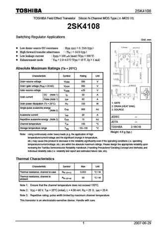
2SK4108 TOSHIBA Field Effect Transistor Silicon N-Channel MOS Type ( -MOS VI) 2SK4108 Switching Regulator Applications Unit mm Low drain-source ON resistance RDS (ON) = 0. 21 (typ.) High forward transfer admittance Yfs = 14 S (typ.) Low leakage current IDSS = 100 A (max) (VDS = 500 V) Enhancement mode Vth = 2.0 4.0 V (VDS = 10 V, ID = 1 mA) Absolute Max
mp4101.pdf
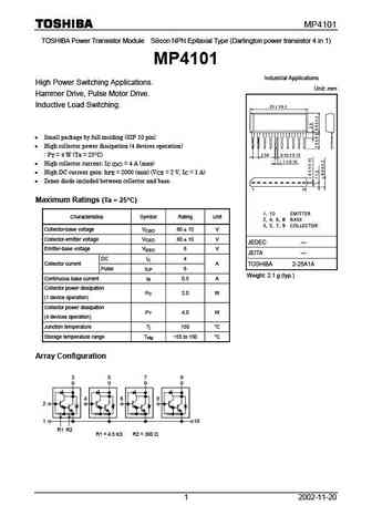
MP4101 TOSHIBA Power Transistor Module Silicon NPN Epitaxial Type (Darlington power transistor 4 in 1) MP4101 Industrial Applications High Power Switching Applications. Unit mm Hammer Drive, Pulse Motor Drive. Inductive Load Switching. Small package by full molding (SIP 10 pin) High collector power dissipation (4 devices operation) P = 4 W (Ta = 25 C) T Hi
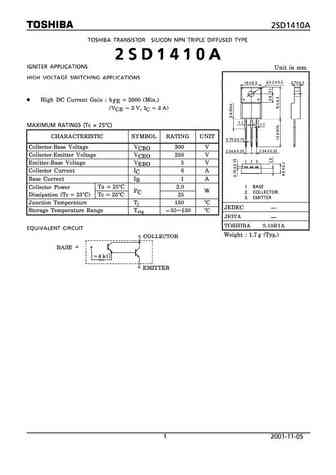
ttd1410b.pdf
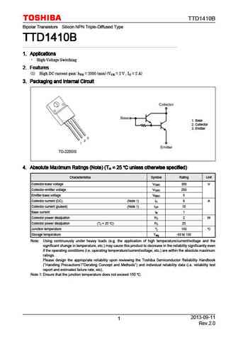
TTD1410B Bipolar Transistors Silicon NPN Triple-Diffused Type TTD1410B TTD1410B TTD1410B TTD1410B 1. Applications 1. Applications 1. Applications 1. Applications High-Voltage Switching 2. Features 2. Features 2. Features 2. Features (1) High DC current gain hFE = 2000 (min) (VCE = 2 V , IC = 2 A) 3. Packaging and Internal Circuit 3. Packaging and Internal Circuit 3. Packa
2sk4103.pdf
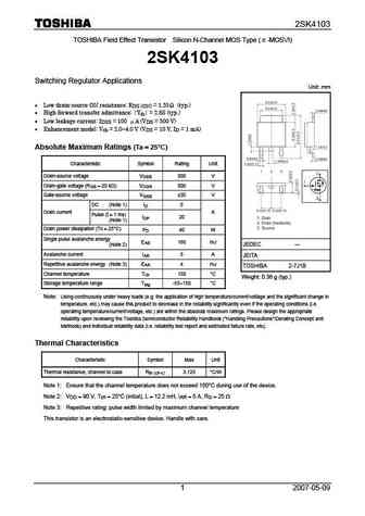
2SK4103 TOSHIBA Field Effect Transistor Silicon N-Channel MOS Type ( -MOSVI) 2SK4103 Switching Regulator Applications Unit mm Low drain-source ON resistance RDS (ON) = 1.35 (typ.) High forward transfer admittance Yfs = 2.8S (typ.) Low leakage current IDSS = 100 A (VDS = 500 V) Enhancement model Vth = 2.0 4.0 V (VDS = 10 V, ID = 1 mA) Absolute Maximu
2sk4107.pdf
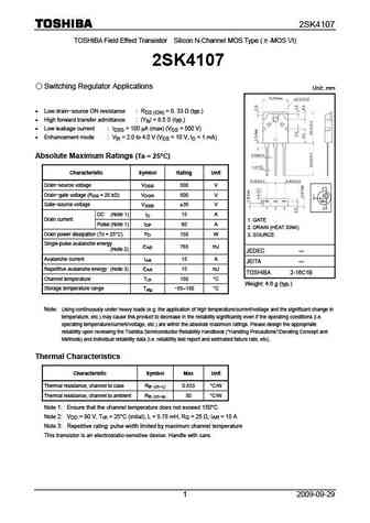
2SK4107 TOSHIBA Field Effect Transistor Silicon N-Channel MOS Type ( -MOS VI) 2SK4107 Switching Regulator Applications Unit mm Low drain-source ON resistance RDS (ON) = 0. 33 (typ.) High forward transfer admittance Yfs = 8.5 S (typ.) Low leakage current IDSS = 100 A (max) (VDS = 500 V) Enhancement mode Vth = 2.0 to 4.0 V (VDS = 10 V, ID = 1
mp4101 .pdf
MP4101 TOSHIBA Power Transistor Module Silicon NPN Epitaxial Type (Four Darlington Power Transistors in One) MP4101 Industrial Applications High Power Switching Applications Unit mm Hammer Drive, Pulse Motor Drive Inductive Load Switching Small package by full molding (SIP 10 pins) High collector power dissipation (4-device operation) PT = 4 W (Ta = 25 C)
ech8410.pdf
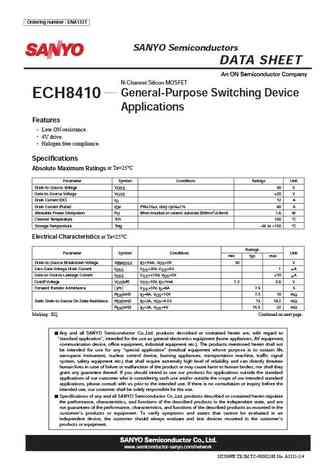
ECH8410 Ordering number ENA1331 SANYO Semiconductors DATA SHEET N-Channel Silicon MOSFET General-Purpose Switching Device ECH8410 Applications Features Low ON-resistance. 4V drive. Halogen free compliance. Specifications at Ta=25 C Absolute Maximum Ratings Parameter Symbol Conditions Ratings Unit Drain-to-Source Voltage VDSS 30 V Gate-to-Source Voltage VGSS 20
2sa1580 2sc4104.pdf
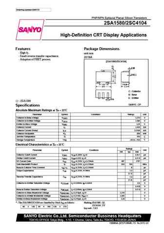
Ordering number EN3172 PNP/NPN Epitaxial Planar Silicon Transistors 2SA1580/2SC4104 High-Definition CRT Display Applications Features Package Dimensions High fT. unit mm Small reverse transfer capacitance. 2018A Adoption of FBET process. [2SA1580/2SC4104] C Collector B Base E Emitter ( ) 2SA1580 SANYO CP Specifications Absolute Maximum Ratings at Ta = 25
2sk4101ls.pdf
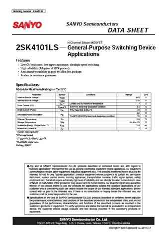
Ordering number ENA0745 2SK4101LS SANYO Semiconductors DATA SHEET N-Channel Silicon MOSFET General-Purpose Switching Device 2SK4101LS Applications Features Low ON-resistance, low input capacitance, ultrahigh-speed switching. High reliability (Adoption of HVP process). Attachment workability is good by Mica-less package. Avalanche resistance guarantee. Specification
2sc4106.pdf

Ordering number EN2471A NPN Triple Diffused Planar Silicon Transistor 2SC4106 400V/7A Switching Regulator Applications Features Package Dimensions High breakdown voltage and high reliability. unit mm Fast switching speed. 2010C Wide ASO. [2SC4106] Adoption of MBIT process. 10.2 4.5 3.6 5.1 1.3 1.2 1 Base 0.8 0.4 2 Collector 1 2 3 3 Emitter JEDEC T
mch3410.pdf
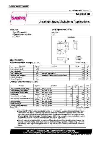
Ordering number ENN6864 MCH3410 N-Channel Silicon MOSFET MCH3410 Ultrahigh-Speed Switching Applications Features Package Dimensions Low ON-resistance. unit mm Ultrahigh-speed switching. 2167 4V drive. [MCH3410] 0.3 0.15 3 1 2 0.65 2.0 1 Gate 2 Source 3 Drain Specifications SANYO MCPH3 Absolute Maximum Ratings at Ta=25 C Parameter Symbol Conditions R
2sc4108.pdf

Ordering number EN2473A NPN Triple Diffused Planar Silicon Transistor 2SC4108 400V/12A Switching Regulator Applications Features Package Dimensions High breakdown voltage and high reliability. unit mm Fast switching speed. 2022A Wide ASO. [2SC4108] Adoption of MBIT process. 15.6 3.2 4.8 14.0 2.0 1.6 1.4 2.0 0.6 1.0 1 2 3 1 Base 0.6 2 Collector 3 E
2sc4107.pdf

Ordering number EN2472A NPN Triple Diffused Planar Silicon Transistor 2SC4107 400V/10A Switching Regulator Applications Features Package Dimensions High breakdown voltage and high reliability. unit mm Fast switching speed. 2010C Wide ASO. [2SC4107] Adoption of MBIT process. 10.2 4.5 3.6 5.1 1.3 1.2 1 Base 0.8 0.4 2 Collector 1 2 3 3 Emitter JEDEC
2sc4109.pdf
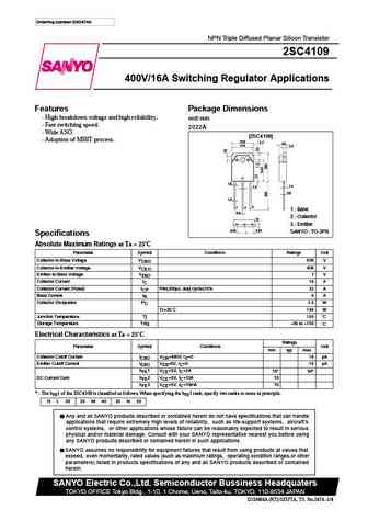
Ordering number EN2474A NPN Triple Diffused Planar Silicon Transistor 2SC4109 400V/16A Switching Regulator Applications Features Package Dimensions High breakdown voltage and high reliability. unit mm Fast switching speed. 2022A Wide ASO. [2SC4109] Adoption of MBIT process. 15.6 3.2 4.8 14.0 2.0 1.6 1.4 2.0 0.6 1.0 1 2 3 1 Base 0.6 2 Collector 3 E
2sk4100ls.pdf
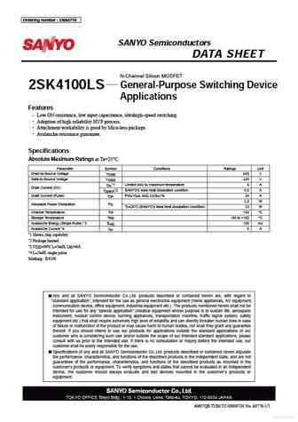
www.DataSheet4U.com Ordering number ENA0778 2SK4100LS SANYO Semiconductors DATA SHEET N-Channel Silicon MOSFET General-Purpose Switching Device 2SK4100LS Applications Features Low ON-resistance, low input capacitance, ultrahigh-speed switching. Adoption of high reliability HVP process. Attachment workability is good by Mica-less package. Avalanche resistance guaran
2sc4105.pdf

Ordering number EN2470A NPN Triple Diffused Planar Silicon Transistor 2SC4105 400V/4A Switching Regulator Applications Features Package Dimensions High breakdown voltage and high reliability. unit mm Fast switching speed. 2010C Wide ASO. [2SC4105] Adoption of MBIT process. 10.2 4.5 3.6 5.1 1.3 1.2 0.8 1 Base 0.4 2 Collector 1 2 3 3 Emitter JEDEC TO
tf410.pdf
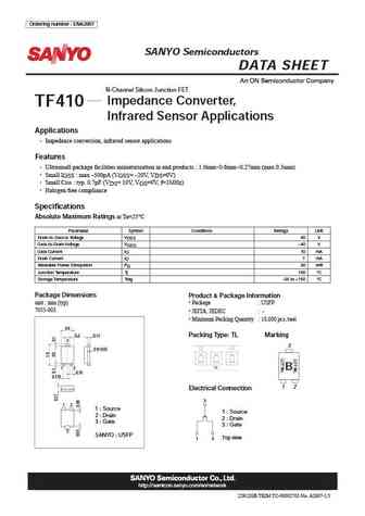
TF410 Ordering number ENA2007 SANYO Semiconductors DATA SHEET N-Channel Silicon Junction FET Impedance Converter, TF410 Infrared Sensor Applications Applications Impedance conversion, infrared sensor applications Features Ultrasmall package facilities miniaturization in end products 1.0mm 0.6mm 0.27mm (max 0.3mm) Small IGSS max --500pA (VGSS= --20V, VDS=0V)
cph3410.pdf
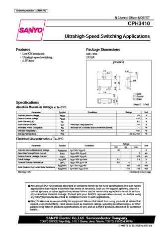
Ordering number ENN6777 CPH3410 N-Channel Silicon MOSFET CPH3410 Ultrahigh-Speed Switching Applications Features Package Dimensions Low ON-resistance. unit mm Ultrahigh-speed switching. 2152A 2.5V drive. [CPH3410] 2.9 0.15 0.4 3 0.05 1 2 1.9 1 Gate 2 Source 3 Drain Specifications SANYO CPH3 Absolute Maximum Ratings at Ta=25 C Parameter Symbol Cond
2sj410.pdf
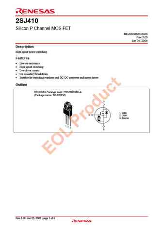
2SJ410 Silicon P Channel MOS FET REJ03G0863-0300 Rev.3.00 Jun 05, 2006 Description High speed power switching Features Low on-resistance High speed switching Low drive current No secondary breakdown Suitable for switching regulator and DC-DC converter and motor driver Outline RENESAS Package code PRSS0003AD-A (Package name TO-220FM) D 1. Gate G
fjv4109r.pdf
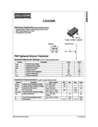
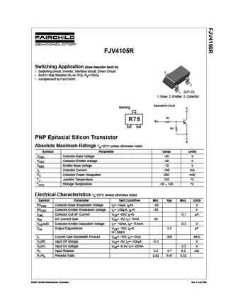
FJV4109R Switching Application (Bias Resistor Built In) Switching circuit, Inverter, Interface circuit, Driver Circuit 3 Built in bias Resistor (R=4.7K ) Complement to FJV3109R 2 SOT-23 1 1. Base 2. Emitter 3. Collector Equivalent Circuit Marking C R79 R B PNP Epitaxial Silicon Transistor E Absolute Maximum Ratings Ta=25 C unless otherwise noted Symbol Parame
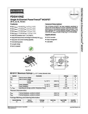
fds4410.pdf
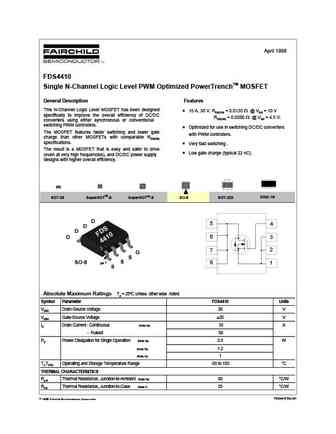
April 1998 FDS4410 Single N-Channel Logic Level PWM Optimized PowerTrenchTM MOSFET General Description Features This N-Channel Logic Level MOSFET has been designed 10 A, 30 V. RDS(ON) = 0.0135 @ VGS = 10 V specifically to improve the overall efficiency of DC/DC RDS(ON) = 0.0200 @ VGS = 4.5 V. converters using either synchronous or conventional switching PWM controllers. O
fdma410nz.pdf

April 2009 FDMA410NZ Single N-Channel 1.5 V Specified PowerTrench MOSFET 20 V, 9.5 A, 23 m Features General Description Max rDS(on) = 23 m at VGS = 4.5 V, ID = 9.5 A This Single N-Channel MOSFET has been designed using Fairchild Semiconductor s advanced Power Trench process to Max rDS(on) = 29 m at VGS = 2.5 V, ID = 8.0 A optimize the rDS(ON) @ VGS = 1.5 V on special M
hp4410dy.pdf
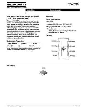
HP4410DY Data Sheet December 2001 10A, 30V, 0.0135 Ohm, Single N-Channel, Features Logic Level Power MOSFET Logic Level Gate Drive This power MOSFET is manufactured using an innovative 10A, 30V process. This advanced process technology achieves the rDS(ON) = 0.0135 at ID = 10A, VGS = 10V lowest possible on-resistance per silicon area, resulting in outstanding perform
fds4410a.pdf
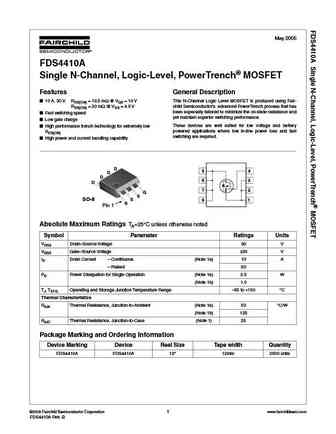
May 2005 FDS4410A Single N-Channel, Logic-Level, PowerTrench MOSFET Features General Description 10 A, 30 V. RDS(ON) = 13.5 m @ VGS = 10 V This N-Channel Logic Level MOSFET is produced using Fair- RDS(ON) = 20 m @ VGS = 4.5 V child Semiconductor s advanced PowerTrench process that has been especially tailored to minimize the on-state resistance and Fast switching speed
fnb41060.pdf

January 2010 TM Motion-SPM FNB41060 Smart Power Module Features General Description It is an advanced motion-smart power module (Motion-SPMTM) 600V-10A 3-phase IGBT inverter bridge including control ICs that Fairchild has newly developed and designed to provide for gate driving and protection very compact and high performance ac motor drives mainly tar- Easy PCB layout due t
fjv4107r.pdf

FJV4107R Switching Application (Bias Resistor Built In) Switching circuit, Inverter, Interface circuit, Driver Circuit 3 Built in bias Resistor (R1=22K , R2=47K ) Complement to FJV3107R 2 SOT-23 1 1. Base 2. Emitter 3. Collector Equivalent Circuit Marking C R1 R77 B R2 PNP Epitaxial Silicon Transistor E Absolute Maximum Ratings Ta=25 C unless otherwise note
nds8410.pdf
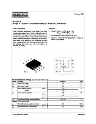
February 1996 NDS8410 Single N-Channel Enhancement Mode Field Effect Transistor General Description Features 10A, 30V. RDS(ON) = 0.015 @ VGS = 10V These N-Channel enhancement mode power field effect RDS(ON) = 0.020 @ VGS = 4.5V. transistors are produced using Fairchild's proprietary, high cell density, DMOS technology. This very high density process is High density cell design
nds9410a.pdf
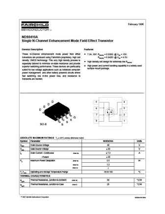
February 1996 NDS9410A Single N-Channel Enhancement Mode Field Effect Transistor General Description Features These N-Channel enhancement mode power field effect 7.3A, 30V. RDS(ON) = 0.028 @ VGS = 10V. transistors are produced using Fairchild's proprietary, high cell RDS(ON) = 0.042 @ VGS = 4.5V. density, DMOS technology. This very high density process is High density cell design
fqs4410tf.pdf
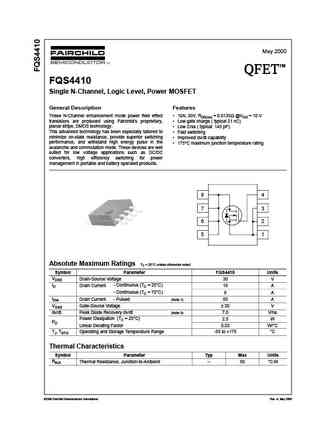
May 2000 TM QFET QFET QFET QFET FQS4410 Single N-Channel, Logic Level, Power MOSFET General Description Features These N-Channel enhancement mode power field effect 10A, 30V, RDS(on) = 0.0135 @VGS = 10 V transistors are produced using Fairchild s proprietary, Low gate charge ( typical 21 nC) planar stripe, DMOS technology. Low Crss ( typical 145 pF) This advanced t
nds8410a.pdf
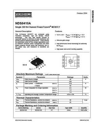
October 2004 NDS8410A Single 30V N-Channel PowerTrench MOSFET General Description Features This N-Channel MOSFET are produced using 10.8 A, 30 V RDS(ON) = 12 m @ VGS = 10 V Fairchild s proprietary, high cell density, DMOS RDS(ON) = 17 m @ VGS = 4.5 V technology. This very high density process is especially tailored to minimize on-state resistance and Ultra-low gate ch
fdmd84100.pdf
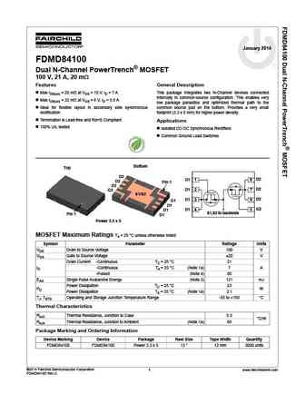
January 2014 FDMD84100 Dual N-Channel PowerTrench MOSFET 100 V, 21 A, 20 m Features General Description Max rDS(on) = 20 m at VGS = 10 V, ID = 7 A This package integrates two N-Channel devices connected internally in common-source configuration. This enables very Max rDS(on) = 32 m at VGS = 6 V, ID = 5.5 A low package parasitics and optimized thermal path to the Ideal fo
fna41060.pdf
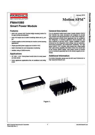
January 2010 TM Motion-SPM FNA41060 Smart Power Module Features General Description It is an advanced motion-smart power module (Motion-SPMTM) 600V-10A 3-phase IGBT inverter bridge including control ICs that Fairchild has newly developed and designed to provide for gate driving and protection very compact and high performance ac motor drives mainly tar- Easy PCB layout due t
ndb410ae ndb410b ndb410be ndp410ae ndp410b vndp410be.pdf
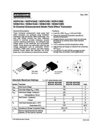
May 1994 NDP410A / NDP410AE / NDP410B / NDP410BE NDB410A / NDB410AE / NDB410B / NDB410BE N-Channel Enhancement Mode Field Effect Transistor General Description Features These N-channel enhancement mode power field 9 and 8A, 100V. RDS(ON) = 0.25 and 0.30 . effect transistors are produced using Fairchild's Critical DC electrical parameters specified at proprietary, high cell density
fjv4103r.pdf

FJV4103R Switching Application (Bias Resistor Built In) Switching circuit, Inverter, Interface circuit, Driver Circuit 3 Built in bias Resistor (R1=22K , R2=22K ) Complement to FJV3103R 2 SOT-23 1 1. Base 2. Emitter 3. Collector Equivalent Circuit C Marking R1 B R73 R2 PNP Epitaxial Silicon Transistor E Absolute Maximum Ratings Ta=25 C unless otherwise noted
fdg410nz.pdf
March 2009 FDG410NZ Single N-Channel PowerTrench MOSFET 20 V, 2.2 A, 70 m Features General Description This N-Channel MOSFET has been designed specifically to Max rDS(on) = 70 m at VGS = 4.5 V, ID = 2.2 A improve the overall efficiency of DC/DC converters using either Max rDS(on) = 77 m at VGS = 2.5 V, ID = 2.0 A synchronous or conventional switching PWM controllers. It
2n4410.pdf

Discrete POWER & Signal Technologies 2N4410 C TO-92 B E NPN General Purpose Amplifier This device is designed for use as general purpose amplifiers and switches requiring collector currents to 50 mA. Sourced from Process 16. See 2N5551 for characteristics. Absolute Maximum Ratings* TA = 25 C unless otherwise noted Symbol Parameter Value Units VCEO Collector-Emitter Voltage 80 V V
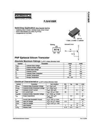
fjv4106r.pdf
FJV4106R Switching Application (Bias Resistor Built In) Switching circuit, Inverter, Interface circuit, Driver Circuit 3 Built in bias Resistor (R1=10K , R2=47K ) Complement to FJV3106R 2 SOT-23 1 1. Base 2. Emitter 3. Collector Equivalent Circuit Marking C R1 R76 B R2 PNP Epitaxial Silicon Transistor E Absolute Maximum Ratings Ta=25 C unless otherwise note
fjv4108r.pdf

FJV4108R Switching Application (Bias Resistor Built In) Switching circuit, Inverter, Interface circuit, Driver Circuit 3 Built in bias Resistor (R1=47K , R2=22K ) Complement to FJV3108R 2 SOT-23 1 1. Base 2. Emitter 3. Collector Equivalent Circuit C Marking R1 B R78 R2 PNP Epitaxial Silicon Transistor E Absolute Maximum Ratings Ta=25 C unless otherwise note
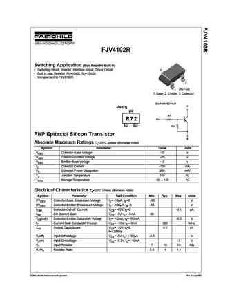
fjv4102r.pdf
FJV4102R Switching Application (Bias Resistor Built In) Switching circuit, Inverter, Interface circuit, Driver Circuit 3 Built in bias Resistor (R1=10K , R2=10K ) Complement to FJV3102R 2 SOT-23 1 1. Base 2. Emitter 3. Collector Equivalent Circuit C Marking R1 B R72 R2 PNP Epitaxial Silicon Transistor E Absolute Maximum Ratings Ta=25 C unless otherwise noted
fjv4105r.pdf
FJV4105R Switching Application (Bias Resistor Built In) Switching circuit, Inverter, Interface circuit, Driver Circuit 3 Built in bias Resistor (R1=4.7K , R2=10K ) Complement to FJV3105R 2 SOT-23 1 1. Base 2. Emitter 3. Collector Equivalent Circuit Marking C R1 R75 B R2 PNP Epitaxial Silicon Transistor E Absolute Maximum Ratings Ta=25 C unless otherwise not
fdme410nzt.pdf
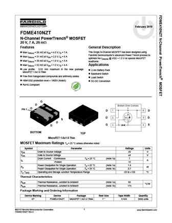
February 2010 FDME410NZT N-Channel PowerTrench MOSFET 20 V, 7 A, 26 m Features General Description This Single N-Channel MOSFET has been designed using Max rDS(on) = 26 m at VGS = 4.5 V, ID = 7 A Fairchild Semiconductor s advanced Power Trench process to Max rDS(on) = 31 m at VGS = 2.5 V, ID = 6 A optimize the rDS(ON) @ VGS = 1.5 V on special MicroFET Max rDS(on) = 39
fdr4410.pdf
April 1998 FDR4410 N-Channel Enhancement Mode Field Effect Transistor General Description Features The FDR4410 has been designed as a smaller, low cost 9.3 A, 30 V. RDS(ON) = 0.013 @ VGS = 10 V alternative to the popular Si4410DY. RDS(ON) = 0.020 @ VGS = 4.5 V. High density cell design for extremely low RDS(ON). The SuperSOTTM-8 package is 40% smaller than the SO-8 package
fdd9410 f085.pdf
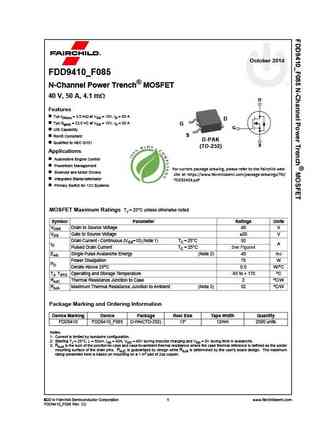
October 2014 FDD9410_F085 N-Channel Power Trench MOSFET 40 V, 50 A, 4.1 m D Features Typ rDS(on) = 3.5 m at VGS = 10V, ID = 50 A D Typ Qg(tot) = 23.5 nC at VGS = 10V, ID = 50 A G G UIS Capability S RoHS Compliant D-PAK TO-252 Qualified to AEC Q101 S (TO-252) Applications Automotive Engine Control Powertrain Management For current package drawing, plea
fjv4104r.pdf

FJV4104R Switching Application (Bias Resistor Built In) Switching circuit, Inverter, Interface circuit, Driver Circuit 3 Built in bias Resistor (R1=47K , R2=47K ) Complement to FJV3104R 2 SOT-23 1 1. Base 2. Emitter 3. Collector Equivalent Circuit C Marking R1 B R74 R2 PNP Epitaxial Silicon Transistor E Absolute Maximum Ratings Ta=25 C unless otherwise note
fjv4101r.pdf

FJV4101R Switching Application (Bias Resistor Built In) Switching circuit, Inverter, Interface circuit, Driver Circuit 3 Built in bias Resistor (R1=4.7K , R2=4.7K ) Complement to FJV3101R 2 SOT-23 1 1. Base 2. Emitter 3. Collector Equivalent Circuit C Marking R1 B R71 R2 PNP Epitaxial Silicon Transistor E Absolute Maximum Ratings Ta=25 C unless otherwise no
ne55410gr.pdf
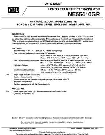
DATA SHEET LDMOS FIELD EFFECT TRANSISTOR NE55410GR N-CHANNEL SILICON POWER LDMOS FET FOR 2 W + 10 W VHF to L-BAND SINGLE-END POWER AMPLIFIER DESCRIPTION The NE55410GR is an N-channel enhancement-mode LDMOS FET designed for driver 0.1 to 2.6 GHz PA, such as, cellular base station amplifier, analog/digital TV-transmitters, and the other PA s. This product has two different FET's on one
pbss9410pa.pdf

Important notice Dear Customer, On 7 February 2017 the former NXP Standard Product business became a new company with the tradename Nexperia. Nexperia is an industry leading supplier of Discrete, Logic and PowerMOS semiconductors with its focus on the automotive, industrial, computing, consumer and wearable application markets In data sheets and application notes which still contain
phpt60410ny.pdf
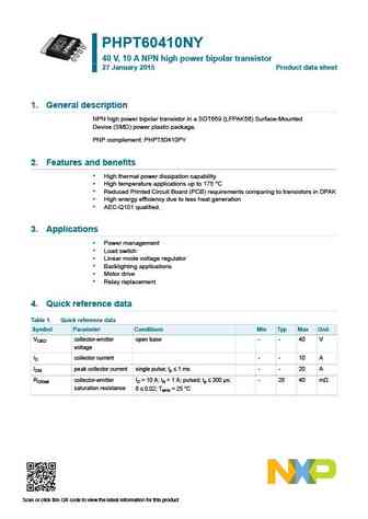
PHPT60410NY 40 V, 10 A NPN high power bipolar transistor 27 January 2015 Product data sheet 1. General description NPN high power bipolar transistor in a SOT669 (LFPAK56) Surface-Mounted Device (SMD) power plastic package. PNP complement PHPT60410PY 2. Features and benefits High thermal power dissipation capability High temperature applications up to 175 C Reduced Print
phpt60410py.pdf
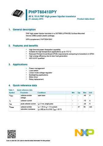
PHPT60410PY 40 V, 10 A PNP high power bipolar transistor 21 January 2015 Product data sheet 1. General description PNP high power bipolar transistor in a SOT669 (LFPAK56) Surface-Mounted Device (SMD) power plastic package. NPN complement PHPT60410NY 2. Features and benefits High thermal power dissipation capability Suitable for high temperature applications up to 175 C
irfu410a.pdf
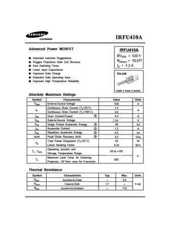
Advanced Power MOSFET IRFU410A BVDSS = 520 V Improved Inductive Ruggedness RDS(on) = 10.0 Rugged Polysilicon Gate Cell Structure Fast Switching Times ID = 1.2 A Lower Input Capacitance Improved Gate Charge Extended Safe Operating Area Improved High Temperature Reliability 1.Gate 2. Drain 3. Source Absolute Maximum Ratings Symbol Characteristic Value Units VDSS Drain-to-
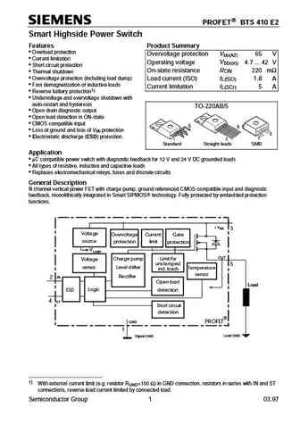
bts410h2.pdf
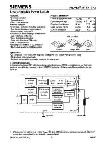
PROFET BTS 410 H2 Smart Highside Power Switch Features Product Summary Overload protection Overvoltage protection Vbb(AZ) 65 V Current limitation V 4.7 ... 42 V Operating voltage bb(on) Short circuit protection On-state resistance R 220 Thermal shutdown ON m Overvoltage protection (including load dump) Load current (ISO) I 1.8 A L(ISO) Fast demagnetiza
bts410f2.pdf
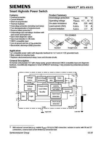
PROFET BTS 410 F2 Smart Highside Power Switch Features Product Summary Overload protection Overvoltage protection Vbb(AZ) 65 V Current limitation V 4.7 ... 42 V Operating voltage bb(on) Short circuit protection On-state resistance R 220 Thermal shutdown ON m Overvoltage protection (including load dump) Load current (ISO) I 1.8 A L(ISO) Fast demagnetiza
bts410g2.pdf
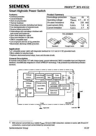
PROFET BTS 410 G2 Smart Highside Power Switch Features Product Summary Overload protection Overvoltage protection Vbb(AZ) 65 V Current limitation V 4.7 ... 42 V Operating voltage bb(on) Short circuit protection On-state resistance R 220 Thermal shutdown ON m Overvoltage protection (including load dump) Load current (ISO) I 1.8 A L(ISO) Fast demagnetiza
bts410d2.pdf

PROFET BTS 410 D2 Smart Highside Power Switch Features Product Summary Overload protection Overvoltage protection Vbb(AZ) 65 V Current limitation V 4.7 ... 42 V Operating voltage bb(on) Short circuit protection On-state resistance R 220 Thermal shutdown ON m Overvoltage protection (including load dump) Load current (ISO) I 1.8 A L(ISO) Fast demagnetiza
bup410d.pdf
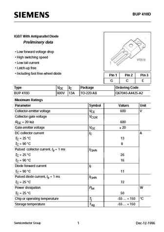
BUP 410D IGBT With Antiparallel Diode Preliminary data Low forward voltage drop High switching speed Low tail current Latch-up free Including fast free-wheel diode Pin 1 Pin 2 Pin 3 G C E Type VCE IC Package Ordering Code BUP 410D 600V 13A TO-220 AB Q67040-A4425-A2 Maximum Ratings Parameter Symbol Values Unit Collector-emitter voltage VCE 600 V Collector-gate
bts410e2.pdf
PROFET BTS 410 E2 Smart Highside Power Switch Features Product Summary Overload protection Overvoltage protection Vbb(AZ) 65 V Current limitation V 4.7 ... 42 V Operating voltage bb(on) Short circuit protection On-state resistance R 220 Thermal shutdown ON m Overvoltage protection (including load dump) Load current (ISO) I 1.8 A L(ISO) Fast demagnetiza
2sc4102 2sc3906k.pdf
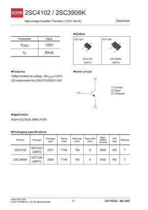
2SC4102 / 2SC3906K Datasheet High-voltage Amplifier Transistor (120V, 50mA) lOutline l Parameter Value SOT-323 SOT-346 VCEO 120V IC 50mA 2SC4102 2SC3906K (UMT3) (SMT3) lFeatures lInner circuit l l 1)High breakdown voltage. (BVCEO=120V) 2)Complements the 2SA1579/2SA1514K.
2sc4102fra.pdf
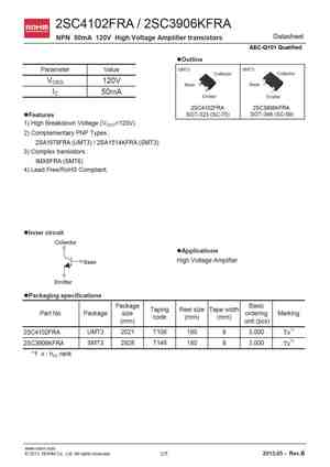
2SC4102 / 2SC3906K 2SC4102FRA / 2SC3906KFRA Datasheet NPN 50mA 120V High Voltage Amplifier transistors AEC-Q101 Qualified lOutline UMT3 SMT3 Parameter Value Collector Collector VCEO 120V Base Base IC 50mA Emitter Emitter 2SC3906K 2SC4102FRA 2SC3906KFRA 2SC4102 SOT-346 (SC-59) SOT-323 (SC-70) lFeatures 1) High Breakdown Voltage (VCEO=120V). 2) Complementary PNP Types 2
2sc4102 2sc3906k 2sc2389s.pdf
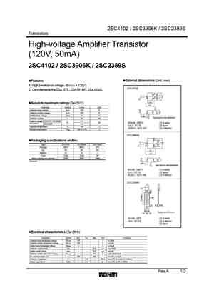
2SC4102 / 2SC3906K / 2SC2389S Transistors High-voltage Amplifier Transistor (120V, 50mA) 2SC4102 / 2SC3906K / 2SC2389S External dimensions (Unit mm) Features 1) High breakdown voltage. (BVCEO = 120V) 2SC4102 2) Complements the 2SA1579 / 2SA1514K / 2SA1038S. 1.25 Absolute maximum ratings (Ta=25 C) 2.1 Parameter Symbol Limits Unit Collector-base voltage VCBO 120 V C
2sc4102.pdf
High-voltage Amplifier Transistor (120V, 50mA) 2SC4102 / 2SC3906K Features Dimensions (Unit mm) 1) High breakdown voltage. (BVCEO = 120V) 2SC4102 2) Complements the 2SA1579 / 2SA1514K 1.25 Absolute maximum ratings (Ta=25 C) 2.1 Parameter Symbol Limits Unit Collector-base voltage VCBO 120 V Collector-emitter voltage VCEO 120 V 0.1Min. Emitter-base voltage VEBO 5 V
tn2410l vn2406d-l vn2410l-ls.pdf
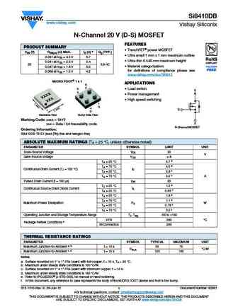
TN2410L, VN2406D/L, VN2410L/LS Vishay Siliconix N-Channel 240-V (D-S) MOSFETs PRODUCT SUMMARY Part Number V(BR)DSS Min (V) rDS(on) Max (W) VGS(th) (V) ID (A) TN2410L 10 @ VGS = 4.5 V 0.5 to 1.8 0.18 VN2406D 6 @ VGS = 10 V 0.8 to 2 1.12 VN2406L 240 6 @ VGS = 10 V 0.8 to 2 0.18 VN2410L 10 @ VGS = 10 V 0.8 to 2 0.18 VN2410LS 10 @ VGS = 10 V 0.8 to 2 0.19 FEATURES BENEFITS APPLICATIONS D
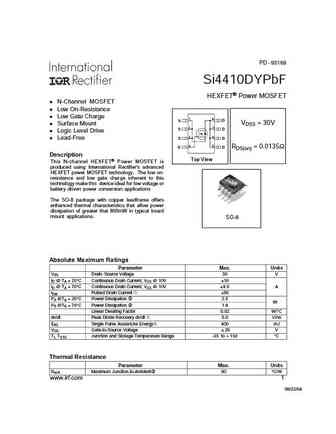
si4410bdy.pdf
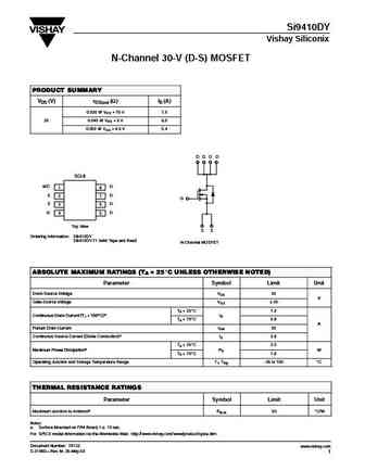
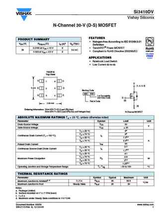
Si4410BDY Vishay Siliconix N-Channel 30-V (D-S) MOSFET FEATURES PRODUCT SUMMARY Halogen-free According to IEC 61249-2-21 VDS (V) RDS(on) ( )ID (A) Definition 0.0135 at VGS = 10 V 10 TrenchFET Power MOSFET 30 0.020 at VGS = 4.5 V 8 100 % Rg Tested Compliant to RoHS Directive 2002/95/EC APPLICATIONS Battery Switch Load Switch SO-8 D S D 1
si4410dypbf si4410dytrpbf.pdf

PD - 95168 Si4410DYPbF HEXFET Power MOSFET l N-Channel MOSFET l Low On-Resistance A l Low Gate Charge A 1 8 S D VDSS = 30V l Surface Mount 2 7 S D l Logic Level Drive 3 6 l Lead-Free S D 4 5 G D RDS(on) = 0.0135 Description Top View This N-channel HEXFET Power MOSFET is produced using International Rectifier's advanced HEXFET power MOSFET technology. The low on- re
si1410edh.pdf
Si1410EDH Vishay Siliconix N-Channel 20 V (D-S) MOSFET FEATURES PRODUCT SUMMARY Halogen-free According to IEC 61249-2-21 VDS (V) RDS(on) ( )ID (A) Definition 0.070 at VGS = 4.5 V 3.7 TrenchFET Power MOSFETs 1.8 V Rated 20 0.080 at VGS = 2.5 V 3.4 ESD Protected 2000 V Thermally Enhanced SC-70 Package 0.100 at VGS = 1.8 V 3.0 Compliant to RoHS Direc
si4102dy.pdf
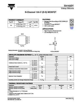
Si4102DY Vishay Siliconix N-Channel 100-V (D-S) MOSFET FEATURES PRODUCT SUMMARY Halogen-free According to IEC 61249-2-21 VDS (V) RDS(on) ( ) ID (A)d Qg (Typ.) Available 0.158 at VGS = 10 V 3.8 TrenchFET Power MOSFET 100 4.6 nC 100 % UIS Tested 0.175 at VGS = 6 V 3.6 APPLICATIONS High Frequency Boost Converter LED Backlight for LCD TV SO-8 S D
sir410dp.pdf
SiR410DP Vishay Siliconix N-Channel 20-V (D-S) MOSFET FEATURES PRODUCT SUMMARY Halogen-free VDS (V) RDS(on) ( ) ID (A)a Qg (Typ.) TrenchFET Power MOSFET 0.0048 at VGS = 10 V 35 100 % Rg Tested 20 12.7 nC 100 % UIS Tested 0.0063 at VGS = 4.5 V 35 APPLICATIONS PowerPAK SO-8 DC/DC Converter - Notebook - POL S 6.15 mm 5.15 mm 1 D S 2 S 3
si4108dy.pdf
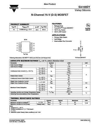
New Product Si4108DY Vishay Siliconix N-Channel 75-V (D-S) MOSFET FEATURES PRODUCT SUMMARY Halogen-free VDS (V) RDS(on) ( ) ID (A)a Qg (Typ.) TrenchFET Power MOSFET RoHS 0.0098 at VGS = 10 V 75 36 nC 20.5 100 % Rg Tested COMPLIANT 100 % UIS Tested APPLICATIONS Primary Side Switch Half Bridge SO-8 Intermediate Bus Converter D S 1
sqj410ep.pdf
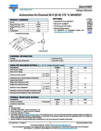
SQJ410EP www.vishay.com Vishay Siliconix Automotive N-Channel 30 V (D-S) 175 C MOSFET FEATURES PRODUCT SUMMARY TrenchFET Power MOSFET VDS (V) 30 AEC-Q101 Qualifiedd RDS(on) ( ) at VGS = 10 V 0.0039 100 % Rg and UIS Tested RDS(on) ( ) at VGS = 4.5 V 0.0042 Material categorization ID (A) 32 For definitions of compliance please see Configuration Single www.
sis410dn.pdf
SiS410DN Vishay Siliconix N-Channel 20 V (D-S) MOSFET FEATURES PRODUCT SUMMARY Halogen-free According to IEC 61249-2-21 VDS (V) RDS(on) ( ) ID (A)a Qg (Typ.) Definition TrenchFET Power MOSFET 0.0048 at VGS = 10 V 35 20 12.7 nC 100 % Rg and UIS Tested 0.0063 at VGS = 4.5 V 35 Compliant to RoHS Directive 2002/95/EC PowerPAK 1212-8 APPLICATIONS DC
sir410d.pdf

SiR410DP Vishay Siliconix N-Channel 20-V (D-S) MOSFET FEATURES PRODUCT SUMMARY Halogen-free VDS (V) RDS(on) ( ) ID (A)a Qg (Typ.) TrenchFET Power MOSFET 0.0048 at VGS = 10 V 35 100 % Rg Tested 20 12.7 nC 100 % UIS Tested 0.0063 at VGS = 4.5 V 35 APPLICATIONS PowerPAK SO-8 DC/DC Converter - Notebook - POL S 6.15 mm 5.15 mm 1 D S 2 S 3
tn2410l vn2406d vn2406l vn2410ls.pdf

TN2410L, VN2406D/L, VN2410L/LS Vishay Siliconix N-Channel 240-V (D-S) MOSFETs PRODUCT SUMMARY Part Number V(BR)DSS Min (V) rDS(on) Max (W) VGS(th) (V) ID (A) TN2410L 10 @ VGS = 4.5 V 0.5 to 1.8 0.18 VN2406D 6 @ VGS = 10 V 0.8 to 2 1.12 VN2406L 240 6 @ VGS = 10 V 0.8 to 2 0.18 VN2410L 10 @ VGS = 10 V 0.8 to 2 0.18 VN2410LS 10 @ VGS = 10 V 0.8 to 2 0.19 FEATURES BENEFITS APPLICATIONS D
si4410dy.pdf
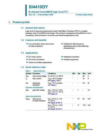
SI4410DY N-channel TrenchMOS logic level FET Rev. 03 4 December 2009 Product data sheet 1. Product profile 1.1 General description Logic level N-channel enhancement mode Field-Effect Transistor (FET) in a plastic package using TrenchMOS technology. This product is designed and qualified for use in computing, communications, consumer and industrial applications only. 1.2 Features a
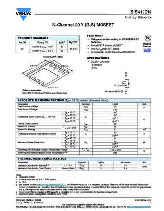
si6410dq.pdf
Si6410DQ Vishay Siliconix N-Channel 30-V (D-S) MOSFET FEATURES PRODUCT SUMMARY Halogen-free VDS (V) RDS(on) ( )ID (A) TrenchFET Power MOSFETs 0.014 at VGS = 10 V 7.8 30 RoHS 0.021 at VGS = 4.5 V 6.3 COMPLIANT D TSSOP-8 * Source Pins 2, 3, 6 and 7 must be tied common. G D D 1 8 S S 2 7 Si6410DQ S S 3 6 G D 4 5 Top View S* Ordering Information
sqa410ej.pdf
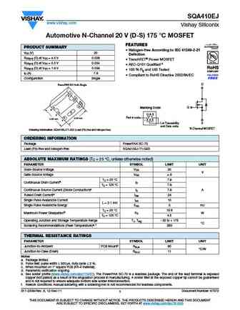
SQA410EJ www.vishay.com Vishay Siliconix Automotive N-Channel 20 V (D-S) 175 C MOSFET FEATURES PRODUCT SUMMARY Halogen-free According to IEC 61249-2-21 VDS (V) 20 Definition RDS(on) ( ) at VGS = 4.5 V 0.028 TrenchFET Power MOSFET RDS(on) ( ) at VGS = 2.5 V 0.034 AEC-Q101 Qualified d RDS(on) ( ) at VGS = 1.8 V 0.038 100 % Rg and UIS Tested ID (A) 7.8
si4101dy.pdf
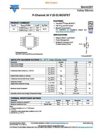
New Product Si4101DY Vishay Siliconix P-Channel 30 V (D-S) MOSFET FEATURES PRODUCT SUMMARY TrenchFET Power MOSFET VDS (V) RDS(on) ( ) Max. ID (A)d Qg (Typ.) 100 % Rg and UIS Tested 0.0060 at VGS = - 10 V - 25.7 Material categorization - 30 65 nC For definitions of compliance please see 0.0080 at VGS = - 4.5 V - 22.3 www.vishay.com/doc?99912 SO-8 APPLICATIONS
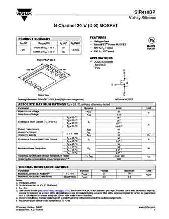
si4100dy.pdf

Si4100DY Vishay Siliconix N-Channel 100-V (D-S) MOSFET FEATURES PRODUCT SUMMARY Halogen-free According to IEC 61249-2-21 VDS (V) RDS(on) ( ) ID (A)d Qg (Typ.) Available 0.063 at VGS = 10 V 6.8 TrenchFET Power MOSFET 100 9 nC 100 % UIS Tested 0.084 at VGS = 6 V 5.8 APPLICATIONS High Frequency Boost Converter LED Backlight for LCD TV SO-8 S D
si4104dy.pdf
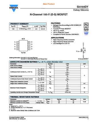
New Product Si4104DY Vishay Siliconix N-Channel 100-V (D-S) MOSFET FEATURES PRODUCT SUMMARY Halogen-free According to IEC 61249-2-21 VDS (V) RDS(on) ( ) ID (A)a Qg (Typ.) Definition 0.105 at VGS = 10 V TrenchET Power MOSFET 100 4.6 8.5 nC 100 % Rg Tested 100 % Avalanche Tested Compliant to RoHS Directive 2002/95/EC APPLICATIONS SO-8 High Freque
sq4410ey.pdf
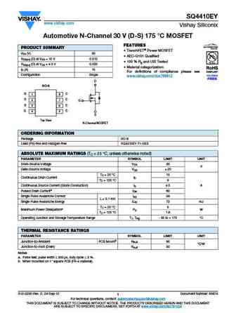
SQ4410EY www.vishay.com Vishay Siliconix Automotive N-Channel 30 V (D-S) 175 C MOSFET FEATURES PRODUCT SUMMARY TrenchFET Power MOSFET VDS (V) 30 AEC-Q101 Qualified RDS(on) ( ) at VGS = 10 V 0.012 100 % Rg and UIS Tested RDS(on) ( ) at VGS = 4.5 V 0.020 Material categorization ID (A) 15 For definitions of compliance please see Configuration Single www
si3410dv.pdf
Si3410DV Vishay Siliconix N-Channel 30-V (D-S) MOSFET FEATURES PRODUCT SUMMARY Halogen-free According to IEC 61249-2-21 VDS (V) RDS(on) ( ) ID (A)a Qg (Typ.) Definition 0.0195 at VGS = 10 V 8 TrenchFET Power MOSFET 30 9.2 nC Compliant to RoHS Directive 2002/95/EC 0.023 at VGS = 4.5 V 8 APPLICATIONS Notebook Load Switch Low Current dc-to-dc TSOP-6 T
sis410n.pdf

SiS410DN Vishay Siliconix N-Channel 20-V (D-S) MOSFET FEATURES PRODUCT SUMMARY Halogen-free VDS (V) RDS(on) ( ) ID (A)a Qg (Typ.) TrenchFET Power MOSFET RoHS 0.0048 at VGS = 10 V 35 100 % Rg Tested COMPLIANT 20 12.7 nC 100 % UIS Tested 0.0063 at VGS = 4.5 V 35 APPLICATIONS PowerPAK 1212-8 DC/DC Converter - Notebook S - POL 3.30 mm 3.30 m
sib410dk.pdf
New Product SiB410DK Vishay Siliconix N-Channel 30 V (D-S) MOSFET FEATURES PRODUCT SUMMARY Halogen-free According to IEC 61249-2-21 VDS (V) RDS(on) ( ) ID (A)a Qg (Typ.) Definition 0.042 at VGS = 4.5 V TrenchFET Power MOSFET 9 100 % Rg Tested 0.046 at VGS = 2.5 V 30 9 5.7 nC Compliant to RoHS Directive 2002/95/EC 0.052 at VGS = 1.8 V 9 APPLICATIONS P
si5410du.pdf
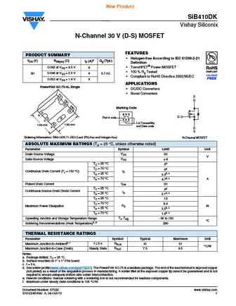
New Product Si5410DU Vishay Siliconix N-Channel 40-V (D-S) MOSFET FEATURES PRODUCT SUMMARY Halogen-free VDS (V) RDS(on) ( ) ID (A)a Qg (Typ.) TrenchFET Power MOSFET 0.018 at VGS = 10 V 12 New Thermally Enhanced PowerPAK RoHS 40 10 nC 0.021 at VGS = 4.5 V 12 COMPLIANT ChipFET Package - Small Footprint Area PowerPAK ChipFET Single - Low On-Resistance
vp2410l.pdf
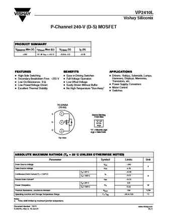
VP2410L Vishay Siliconix P-Channel 240-V (D-S) MOSFET PRODUCT SUMMARY V(BR)DSS Min (V) rDS(on) Max (W) VGS(th) (V) ID (A) 240 10 @ VGS = 4.5 V 0.8 to 2.5 0.18 FEATURES BENEFITS APPLICATIONS D High-Side Switching D Ease in Driving Switches D Drivers Relays, Solenoids, Lamps, Hammers, Displays, Memories, D Secondary Breakdown Free 255 V D Full-Voltage Operation Trans
sq3410ev.pdf
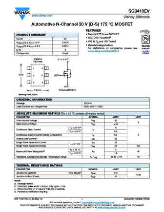
SQ3410EV www.vishay.com Vishay Siliconix Automotive N-Channel 30 V (D-S) 175 C MOSFET FEATURES TrenchFET Power MOSFET PRODUCT SUMMARY AEC-Q101 Qualifiedd VDS (V) 30 100 % Rg and UIS Tested RDS(on) ( ) at VGS = 10 V 0.0175 Material categorization RDS(on) ( ) at VGS = 4.5 V 0.0213 For definitions of compliance please see ID (A) 8 www.vishay.com/doc?99912
ctlm3410-ctlm7410-ctlm3474-m832d.pdf
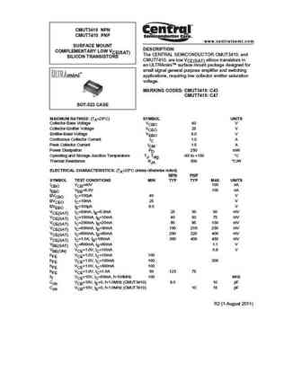
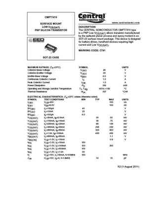
CTLM3410-M832D CTLM7410-M832D CTLM3474-M832D www.centralsemi.com SURFACE MOUNT DESCRIPTION DUAL, LOW VCE (SAT) The CENTRAL SEMICONDUCTOR CTLM3410-M832D SILICON TRANSISTORS (Dual NPN), CTLM7410-M832D (Dual PNP), and CTLM3474-M832D (Complementary NPN & PNP) are Low VCE(SAT) Transistors packaged in the small, thermally efficient, 3x2mm Tiny Leadless Module (TLM ) surface mount
cmut3410.pdf

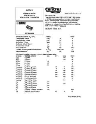
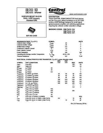
CMUT3410 NPN CMUT7410 PNP www.centralsemi.com SURFACE MOUNT DESCRIPTION COMPLEMENTARY LOW VCE(SAT) The CENTRAL SEMICONDUCTOR CMUT3410, and SILICON TRANSISTORS CMUT7410, are low VCE(SAT) silicon transistors in an ULTRAmini surface mount package designed for small signal general purpose amplifier and switching applications, requiring low collector emitter saturation voltage.
cmst3410.pdf
CMST3410 NPN CMST7410 PNP www.centralsemi.com SURFACE MOUNT COMPLEMENTARY LOW VCE(SAT) DESCRIPTION The CENTRAL SEMICONDUCTOR CMST3410, SILICON TRANSISTORS CMST7410 types are complementary silicon transistors manufactured by the epitaxial planar process, epoxy molded in a SUPERmini surface mount package, designed for battery driven, handheld devices requiring high current and
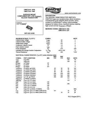
cmpt3410.pdf
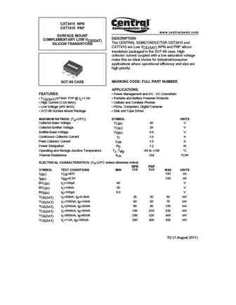
CMPT3410 www.centralsemi.com SURFACE MOUNT LOW VCE(SAT) DESCRIPTION NPN SILICON TRANSISTOR The CENTRAL SEMICONDUCTOR CMPT3410 type is a NPN Low VCE(SAT) silicon transistor manufactured by the epitaxial planar process and epoxy molded in an SOT-23 surface mount package. This device is designed for battery driven, handheld devices requiring high current and Low VCE(SAT). MARKING
ctlm3410 ctlm7410 ctlm3474-m832d.pdf
CTLM3410-M832D CTLM7410-M832D CTLM3474-M832D www.centralsemi.com SURFACE MOUNT DESCRIPTION DUAL, LOW VCE (SAT) The CENTRAL SEMICONDUCTOR CTLM3410- SILICON TRANSISTORS M832D (Dual NPN), CTLM7410-M832D (Dual PNP), and CTLM3474-M832D (Complementary NPN & PNP) are Low VCE(SAT) Transistors packaged in the small, thermally efficient, 3x2mm Tiny Leadless Module (TLM ) surface mount
cmut7410.pdf
CMUT3410 NPN CMUT7410 PNP www.centralsemi.com SURFACE MOUNT DESCRIPTION COMPLEMENTARY LOW VCE(SAT) The CENTRAL SEMICONDUCTOR CMUT3410, and SILICON TRANSISTORS CMUT7410, are low VCE(SAT) silicon transistors in an ULTRAmini surface mount package designed for small signal general purpose amplifier and switching applications, requiring low collector emitter saturation voltage.
cmpt7410.pdf
CMPT7410 www.centralsemi.com SURFACE MOUNT LOW VCE(SAT) DESCRIPTION The CENTRAL SEMICONDUCTOR CMPT7410 type PNP SILICON TRANSISTOR is a PNP Low VCE(SAT) silicon transistor manufactured by the epitaxial planar process and epoxy molded in an SOT-23 surface mount package. This device is designed for battery driven, handheld devices requiring high current and Low VCE(SAT). MARKING
cmst7410.pdf

CMST3410 NPN CMST7410 PNP www.centralsemi.com SURFACE MOUNT COMPLEMENTARY LOW VCE(SAT) DESCRIPTION The CENTRAL SEMICONDUCTOR CMST3410, SILICON TRANSISTORS CMST7410 types are complementary silicon transistors manufactured by the epitaxial planar process, epoxy molded in a SUPERmini surface mount package, designed for battery driven, handheld devices requiring high current and
cmlt7410.pdf
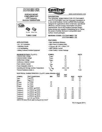
CMLT3410 NPN CMLT7410 PNP CMLT3474 NPN/PNP www.centralsemi.com SURFACE MOUNT SILICON DESCRIPTION DUAL, LOW VCE(SAT) These CENTRAL SEMICONDUCTOR dual devices TRANSISTORS are low VCE(SAT) silicon transistors in an SOT-563 surface mount package designed for small signal general purpose amplifier and switching applications requiring low collector emitter saturation voltage. MARKIN
ctlt3410-ctlt7410-m621.pdf
CTLT3410-M621 (NPN) CTLT7410-M621 (PNP) www.centralsemi.com SURFACE MOUNT COMPLEMENTARY DESCRIPTION LOW VCE(SAT) The CENTRAL SEMICONDUCTOR CTLT3410-M621 SILICON TRANSISTORS and CTLT7410-M621 are Low VCE(SAT) transistors in a very small leadless 1x2mm surface mount package, designed for applications where small size, operational efficiency, and low energy consumption are prime
cxt3410 cxt7410.pdf
CXT3410 NPN CXT7410 PNP www.centralsemi.com SURFACE MOUNT COMPLEMENTARY LOW VCE(SAT) DESCRIPTION The CENTRAL SEMICONDUCTOR CXT3410 and SILICON TRANSISTORS CXT7410 are Low VCE(SAT) NPN and PNP silicon transistors packaged in the SOT-89 case. High collector current coupled with a low saturation voltage make this an ideal choice for industrial/consumer applications where operation
cmlt3410.pdf

CMLT3410 NPN CMLT7410 PNP CMLT3474 NPN/PNP www.centralsemi.com SURFACE MOUNT SILICON DESCRIPTION DUAL, LOW VCE(SAT) These CENTRAL SEMICONDUCTOR dual devices TRANSISTORS are low VCE(SAT) silicon transistors in an SOT-563 surface mount package designed for small signal general purpose amplifier and switching applications requiring low collector emitter saturation voltage. MARKIN
zvp4105astoa zvp4105astob zvp4105astz.pdf
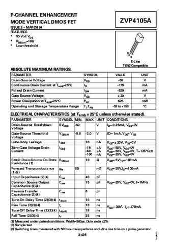
P-CHANNEL ENHANCEMENT ZVP4105A MODE VERTICAL DMOS FET ISSUE 2 MARCH 94 T V I VD D I D E-Line TO92 Compatible ABSOLUTE MAXIMUM RATINGS. T V IT D i V I VD V i D i T ID I D i ID V I V V Di i i T i T T T ELECTRICAL CHARACTERISTICS (at Tamb = 25 C unless otherwise stated). T I IT DITI D i VD V ID V V V I T I V 8 V ID VD V V I I
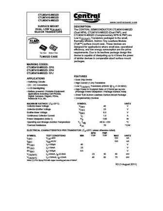
bcp54ta bcp5410ta bcp5416ta bcp5416qta bcp55ta bcp5510ta bcp5516ta bcp56ta bcp5610ta bcp5616ta bcp5616tc bcp5616qta bcp5616qtc.pdf
BCP 54/ 55/ 56 NPN MEDIUM POWER TRANSISTORS IN SOT223 Features Mechanical Data BVCEO > 45V, 60V & 80V Case SOT223 IC = 1A High Continuous Collector Current Case Material Molded Plastic. Green Molding Compound; ICM = 2A Peak Pulse Current UL Flammability Rating 94V-0 2W Power Dissipation Moisture Sensitivity Level 1 per J-STD-020 Low Saturat
zvn4106f.pdf
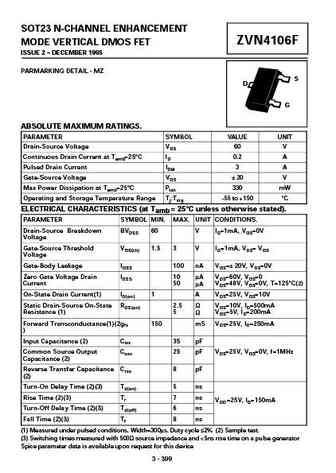
SOT23 N-CHANNEL ENHANCEMENT ZVN4106F MODE VERTICAL DMOS FET ISSUE 2 DECEMBER 1995 PARMARKING DETAIL - MZ S D G ABSOLUTE MAXIMUM RATINGS. PARAMETER SYMBOL VALUE UNIT V Drain-Source Voltage VDS 60 V Continuous Drain Current at Tamb=25 C ID 0.2 A 10 Pulsed Drain Current IDM 3A Gate-Source Voltage VGS 20 V Max Power Dissipation at Tamb=25 C Ptot 330 mW ent Operating and St
zvn4106fta zvn4106ftc.pdf
A Product Line of Diodes Incorporated ZVN4106F 60V N-CHANNEL ENHANCEMENT MODE VERTICAL DMOSFET IN SOT23 Features Mechanical Data BVDSS > 60V Case SOT23 Case Material Molded Plastic, Green Molding Compound. UL RDS(on) 2.5 @ VGS = 10V Flammability Classification Rating 94V-0 Maximum continuous drain current ID = 200mA Moisture Sensitivity Lev
dmg7410sfg.pdf
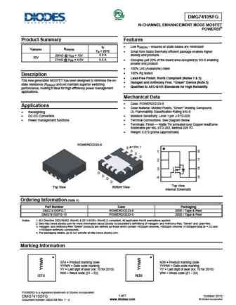
DMG7410SFG Green N-CHANNEL ENHANCEMENT MODE MOSFET POWERDI Product Summary Features Low RDS(ON) ensures on state losses are minimized ID V(BR)DSS RDS(ON) TA = 25 C Small form factor thermally efficient package enables higher 20m @ VGS = 10V 8.0 A density end products 30V 27m @ VGS = 4.5V 6.5 A Occupies just 33% of the board area occupied by SO-8
zvp4105a.pdf

P-CHANNEL ENHANCEMENT ZVP4105A MODE VERTICAL DMOS FET ISSUE 2 MARCH 94 T V I VD D I D E-Line TO92 Compatible ABSOLUTE MAXIMUM RATINGS. T V IT D i V I VD V i D i T ID I D i ID V I V V Di i i T i T T T ELECTRICAL CHARACTERISTICS (at Tamb = 25 C unless otherwise stated). T I IT DITI D i VD V ID V V V I T I V 8 V ID VD V V I I
bcx54ta bcx5410ta bcx5416ta bcx5416-13r bcx55ta bcx5510ta bcx5516ta bcx56ta bcx5610ta bcx5616ta bcx5616tc bcx5410tc bcx5416tc bcx54tc bcx5510tc bcx5516tc bcx55tc bcx5610tc bcx56tc bcx5616qta.pdf
BCX54 /55 /56 NPN MEDIUM POWER TRANSISTORS IN SOT89 Features Mechanical Data BVCEO > 45V, 60V & 80V Case SOT89 Ic = 1A Continuous Collector Current Case Material Molded Plastic, Green Molding Compound; ICM = 2A Peak Pulse Current UL Flammability Rating 94V-0 Low Saturation Voltage VCE(sat)
auirlr3410.pdf
AUTOMOTIVE GRADE AUIRLR3410 Features HEXFET Power MOSFET Advanced Planar Technology Low On-Resistance VDSS 100V Logic Level Gate Drive Dynamic dV/dT Rating RDS(on) max. 105m 175 C Operating Temperature Fast Switching ID 17A Fully Avalanche Rated Repetitive Avalanche Allowed up to Tjmax Lead-Free, RoHS Compliant D
irfi4410zpbf.pdf
IRFI4410ZPbF HEXFET Power MOSFET Applications VDSS 100V High Efficiency Synchronous Rectification in SMPS Uninterruptible Power Supply RDS(on) typ. 7.9m High Speed Power Switching Hard Switched and High Frequency Circuits RDS(on) max. 9.3m ID 43A Benefits Improved Gate, Avalanche and Dynamic dV/dt Ruggedness Fully Characterized Capac
bfp410.pdf
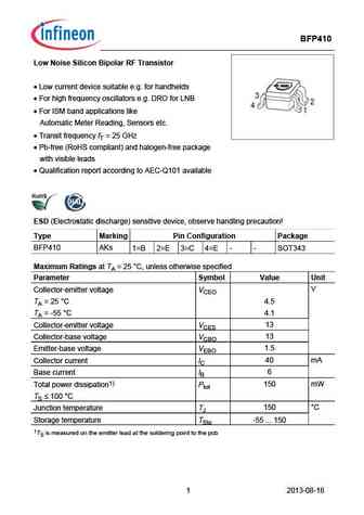
BFP410 Low Noise Silicon Bipolar RF Transistor Low current device suitable e.g. for handhelds 3 For high frequency oscillators e.g. DRO for LNB 2 4 1 For ISM band applications like Automatic Meter Reading, Sensors etc. Transit frequency fT = 25 GHz Pb-free (RoHS compliant) and halogen-free package with visible leads Qualification report according to AEC-Q1
auirfr5410.pdf
AUTOMOTIVE GRADE AUIRFR5410 Features HEXFET Power MOSFET Advanced Planar Technology VDSS -100V P-Channel MOSFET Low On-Resistance RDS(on) max. 0.205 Dynamic dV/dT Rating 175 C Operating Temperature ID -13A Fast Switching Fully Avalanche Rated Repetitive Avalanche Allowed up to Tjmax Lead-Free, RoHS Compliant D Aut
si4410dypbf.pdf
PD - 95168 Si4410DYPbF HEXFET Power MOSFET l N-Channel MOSFET l Low On-Resistance A l Low Gate Charge A 1 8 S D VDSS = 30V l Surface Mount 2 7 S D l Logic Level Drive 3 6 l Lead-Free S D 4 5 G D RDS(on) = 0.0135 Description Top View This N-channel HEXFET Power MOSFET is produced using International Rectifier's advanced HEXFET power MOSFET technology. The low on- re
ipp410n30n.pdf
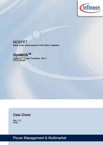
MOSFET Metal Oxide Semiconductor Field Effect Transistor OptiMOSTM OptiMOSTM Power-Transistor, 300 V IPP410N30N Data Sheet Rev. 2.0 Final Power Management & Multimarket OptiMOSTM Power-Transistor, 300 V IPP410N30N TO-220-3 1 Description tab Features N-channel, normal level Fast Diode with reduced Q rr Optimized for hard commutation ruggedness Very low on-resi
auirf4104 auirf4104s.pdf
AUIRF4104 AUTOMOTIVE GRADE AUIRF4104S Features HEXFET Power MOSFET Advanced Process Technology VDSS 40V Ultra Low On-Resistance RDS(on) typ. 4.3m 175 C Operating Temperature Fast Switching max. 5.5m Fully Avalanche Rated ID (Silicon Limited) 120A Repetitive Avalanche Allowed up to Tjmax ID (Package Limited) 75A L
auirfr4104 auirfu4104.pdf

AUIRFR4104 AUTOMOTIVE GRADE AUIRFU4104 Features HEXFET Power MOSFET Advanced Process Technology Low On-Resistance VDSS 40V 175 C Operating Temperature RDS(on) max. 5.5m Fast Switching Repetitive Avalanche Allowed up to Tjmax ID (Silicon Limited) 119A Lead-Free, RoHS Compliant Automotive Qualified * ID (Package Limited) 42A D
auirfr4105z auirfu4105z.pdf
AUIRFR4105Z AUTOMOTIVE GRADE AUIRFU4105Z Features HEXFET Power MOSFET Advanced Process Technology Ultra Low On-Resistance VDSS 55V 175 C Operating Temperature Fast Switching RDS(on) max. 24.5m Repetitive Avalanche Allowed up to Tjmax Lead-Free, RoHS Compliant ID 30A Automotive Qualified * D D Description Specifically designed
irfl4105pbf.pdf
IRFL4105PbF Surface Mount HEXFET Power MOSFET Advanced Process Technology Ultra Low On-Resistance VDSS 55V Dynamic dv/dt Rating RDS(on) 0.045 Fast Switching Fully Avalanche Rated ID 3.7A Lead-Free Description Fifth Generation HEXFETs from International Rectifier utilize advanced processing techniques to achieve extremely low on- resi
oms410.pdf
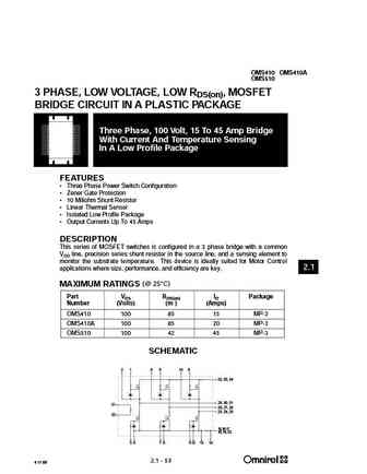
OMS410 OMS410A OMS510 3 PHASE, LOW VOLTAGE, LOW RDS(on), MOSFET BRIDGE CIRCUIT IN A PLASTIC PACKAGE Three Phase, 100 Volt, 15 To 45 Amp Bridge With Current And Temperature Sensing In A Low Profile Package FEATURES Three Phase Power Switch Configuration Zener Gate Protection 10 Miliohm Shunt Resistor Linear Thermal Sensor Isolated Low Profile Package Output C
nvb6410an.pdf
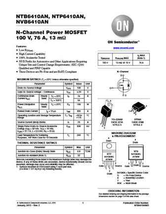
NTB6410AN, NTP6410AN, NVB6410AN N-Channel Power MOSFET 100 V, 76 A, 13 mW Features www.onsemi.com Low RDS(on) High Current Capability ID MAX 100% Avalanche Tested V(BR)DSS RDS(ON) MAX (Note 1) NVB Prefix for Automotive and Other Applications Requiring 100 V 13 mW @ 10 V 76 A Unique Site and Control Change Requirements; AEC-Q101 Qualified and PPAP Capable N-Channel
ntb6410ang ntp6410ang.pdf
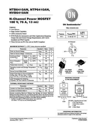
NTB6410AN, NTP6410AN, NVB6410AN N-Channel Power MOSFET 100 V, 76 A, 13 mW Features http //onsemi.com Low RDS(on) High Current Capability ID MAX 100% Avalanche Tested V(BR)DSS RDS(ON) MAX (Note 1) NVB Prefix for Automotive and Other Applications Requiring 100 V 13 mW @ 10 V 76 A Unique Site and Control Change Requirements; AEC-Q101 Qualified and PPAP Capable N-Chan
ntmfs4108n.pdf
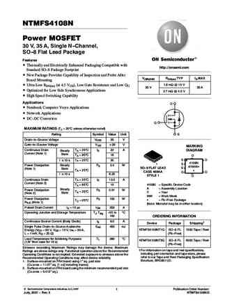
NTMFS4108N Power MOSFET 30 V, 35 A, Single N-Channel, SO-8 Flat Lead Package http //onsemi.com Features Thermally and Electrically Enhanced Packaging Compatible with http //onsemi.com Standard SO-8 Package Footprint New Package Provides Capability of Inspection and Probe After V(BR)DSS RDS(on) TYP ID MAX Board Mounting 1.8 mW @ 10 V Ultra Low RDS(on) (at 4.5 VGS), Low G
ntb6410an ntp6410an.pdf
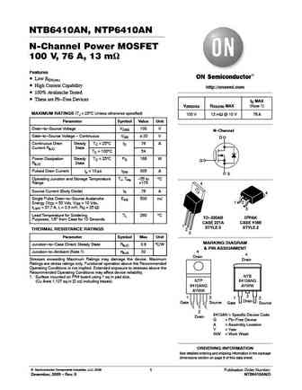
NTB6410AN, NTP6410AN N-Channel Power MOSFET 100 V, 76 A, 13 mW Features Low RDS(on) High Current Capability http //onsemi.com 100% Avalanche Tested These are Pb-Free Devices ID MAX V(BR)DSS RDS(ON) MAX (Note 1) MAXIMUM RATINGS (TJ = 25 C Unless otherwise specified) 100 V 13 mW @ 10 V 76 A Parameter Symbol Value Unit Drain-to-Source Voltage VDSS 100 V N-Channel G
ntms4107n-d ntms4107nr2g.pdf
NTMS4107N Power MOSFET 30 V, 18 A, Single N-Channel, SO-8 Features Ultra Low RDS(on) (at 4.5 VGS), Low Gate Resistance and Low QG Optimized for Low Side Synchronous Applications http //onsemi.com High Speed Switching Capability Pb-Free Package is Available V(BR)DSS RDS(on) TYP ID MAX 3.4 mW @ 10 V Applications 30 V 18 A Notebook Computer Vcore Applications 4.7
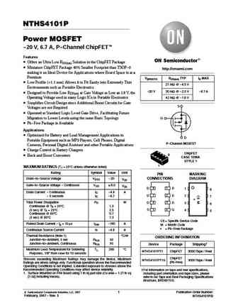
ntjd4105c.pdf
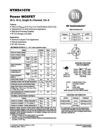
NTJD4105C Small Signal MOSFET 20 V / -8.0 V, Complementary, +0.63 A / -0.775 A, SC-88 Features Complementary N and P Channel Device Leading -8.0 V Trench for Low RDS(on) Performance http //onsemi.com ESD Protected Gate - ESD Rating Class 1 SC-88 Package for Small Footprint (2 x 2 mm) V(BR)DSS RDS(on) TYP ID Max Pb-Free Packages are Available 0.29 W @ 4.5 V N-Ch
ntb6410an ntp6410an nvb6410an.pdf

NTB6410AN, NTP6410AN, NVB6410AN N-Channel Power MOSFET 100 V, 76 A, 13 mW Features www.onsemi.com Low RDS(on) High Current Capability ID MAX 100% Avalanche Tested V(BR)DSS RDS(ON) MAX (Note 1) NVB Prefix for Automotive and Other Applications Requiring 100 V 13 mW @ 10 V 76 A Unique Site and Control Change Requirements; AEC-Q101 Qualified and PPAP Capable N-Channel
nts4101p.pdf

NTS4101P Power MOSFET -20 V, -1.37 A, Single P-Channel, SC-70 Features Leading -20 V Trench for Low RDS(on) http //onsemi.com -2.5 V Rated for Low Voltage Gate Drive V(BR)DSS RDS(on) Typ ID Max SC-70 Surface Mount for Small Footprint (2x2 mm) 83 mW @ -4.5 V Pb-Free Package is Available -20 V 88 mW @ -3.6 V -1.37 A Applications High Side Load Switch 104 mW @ -2.5
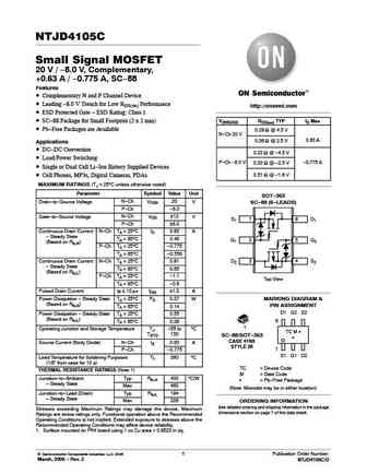
ntmfs5c410n.pdf

MOSFET Single, N-Channel 40 V, 0.92 mW, 300 A NTMFS5C410N Features www.onsemi.com Small Footprint (5x6 mm) for Compact Design Low RDS(on) to Minimize Conduction Losses Low QG and Capacitance to Minimize Driver Losses V(BR)DSS RDS(ON) MAX ID MAX These Devices are Pb-Free and are RoHS Compliant 40 V 0.92 mW @ 10 V 300 A MAXIMUM RATINGS (TJ = 25 C unless otherwise
nvmfs5c410nl.pdf
NVMFS5C410NL Power MOSFET 40 V, 0.9 mW, 315 A, Single N-Channel Features Small Footprint (5x6 mm) for Compact Design Low RDS(on) to Minimize Conduction Losses http //onsemi.com Low QG and Capacitance to Minimize Driver Losses NVMFS5C410NLWF - Wettable Flank Option for Enhanced Optical Inspection V(BR)DSS RDS(ON) MAX ID MAX AEC-Q101 Qualified and PPAP Capable 0.9
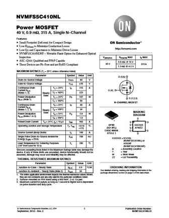
nths4101p-d.pdf
NTHS4101P Power MOSFET -20 V, 6.7 A, P-Channel ChipFETt Features Offers an Ultra Low RDS(on) Solution in the ChipFET Package Miniature ChipFET Package 40% Smaller Footprint than TSOP-6 http //onsemi.com making it an Ideal Device for Applications where Board Space is at a Premium V(BR)DSS RDS(on) TYP ID MAX Low Profile (
ntr4101pt1g.pdf
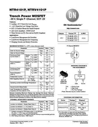
NTR4101P, NTRV4101P Trench Power MOSFET -20 V, Single P-Channel, SOT-23 Features Leading -20 V Trench for Low RDS(on) -1.8 V Rated for Low Voltage Gate Drive http //onsemi.com http //onsemi.com SOT-23 Surface Mount for Small Footprint AEC Q101 Qualified - NTRV4101P These Devices are Pb-Free and are RoHS Compliant V(BR)DSS RDS(ON) TYP ID MAX Applications 70 mW @
vn2410l.pdf
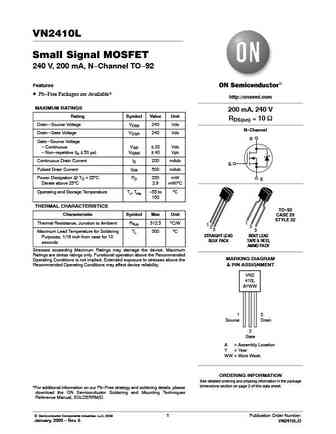
VN2410L Small Signal MOSFET 240 V, 200 mA, N-Channel TO-92 Features Pb-Free Packages are Available* http //onsemi.com MAXIMUM RATINGS 200 mA, 240 V Rating Symbol Value Unit RDS(on) = 10 Drain -Source Voltage VDSS 240 Vdc N-Channel Drain -Gate Voltage VDGR 240 Vdc D Gate-Source Voltage - Continuous VGS 20 Vdc - Non-repetitive (tp 50 s) VGSM 40 Vpk Continuous D
ntjd4105ct1g.pdf
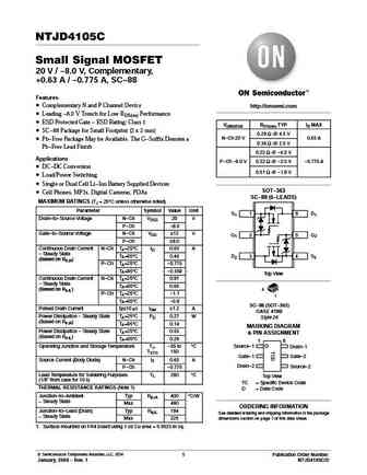
NTJD4105C Small Signal MOSFET 20 V / -8.0 V, Complementary, +0.63 A / -0.775 A, SC-88 Features Complementary N and P Channel Device http //onsemi.com Leading -8.0 V Trench for Low RDS(on) Performance ESD Protected Gate - ESD Rating Class 1 V(BR)DSS RDS(on) TYP ID MAX SC-88 Package for Small Footprint (2 x 2 mm) 0.29 W @ 4.5 V N-Ch 20 V 0.63 A Pb-Free Package M
nts4101pt1.pdf
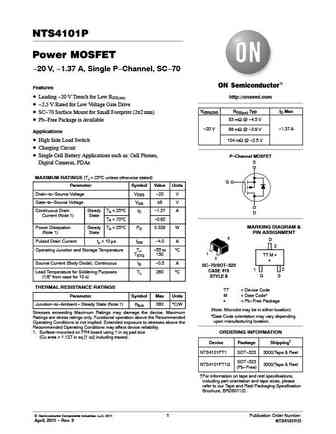
NTS4101P Power MOSFET -20 V, -1.37 A, Single P-Channel, SC-70 Features Leading -20 V Trench for Low RDS(on) http //onsemi.com -2.5 V Rated for Low Voltage Gate Drive V(BR)DSS RDS(on) Typ ID Max SC-70 Surface Mount for Small Footprint (2x2 mm) 83 mW @ -4.5 V Pb-Free Package is Available -20 V 88 mW @ -3.6 V -1.37 A Applications High Side Load Switch 104 mW @ -2.5
ntrv4101p.pdf
NTR4101P, NTRV4101P Trench Power MOSFET -20 V, Single P-Channel, SOT-23 Features Leading -20 V Trench for Low RDS(on) -1.8 V Rated for Low Voltage Gate Drive www.onsemi.com www.onsemi.com SOT-23 Surface Mount for Small Footprint NTRV Prefix for Automotive and Other Applications Requiring Unique Site and Control Change Requirements; AEC-Q101 V(BR)DSS RDS(ON) TYP ID MAX
mmjt9410-d.pdf
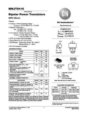
MMJT9410 Preferred Device Bipolar Power Transistors NPN Silicon Features Collector -Emitter Sustaining Voltage - VCEO(sus) = 30 Vdc (Min) @ IC = 10 mAdc http //onsemi.com High DC Current Gain - hFE = 85 (Min) @ IC = 0.8 Adc POWER BJT = 60 (Min) @ IC = 3.0 Adc IC = 3.0 AMPERES Low Collector -Emitter Saturation Voltage - BVCEO = 30 VOLTS VCE(sat) = 0.2 Vdc (Max) @ IC =
ntmfs4108nt1g.pdf
NTMFS4108N Power MOSFET 30 V, 35 A, Single N-Channel, SO-8 Flat Lead Package http //onsemi.com Features Thermally and Electrically Enhanced Packaging Compatible with http //onsemi.com Standard SO-8 Package Footprint New Package Provides Capability of Inspection and Probe After V(BR)DSS RDS(on) TYP ID MAX Board Mounting 1.8 mW @ 10 V Ultra Low RDS(on) (at 4.5 VGS), Low G
fdg410nz.pdf

Is Now Part of To learn more about ON Semiconductor, please visit our website at www.onsemi.com Please note As part of the Fairchild Semiconductor integration, some of the Fairchild orderable part numbers will need to change in order to meet ON Semiconductor s system requirements. Since the ON Semiconductor product management systems do not have the ability to manage part nomenclatur
ntmfs5c410nl.pdf
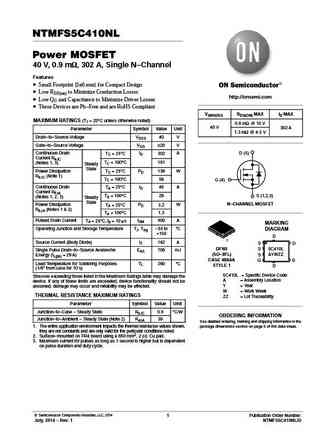
NTMFS5C410NL Power MOSFET 40 V, 0.9 mW, 302 A, Single N-Channel Features Small Footprint (5x6 mm) for Compact Design Low RDS(on) to Minimize Conduction Losses http //onsemi.com Low QG and Capacitance to Minimize Driver Losses These Devices are Pb-Free and are RoHS Compliant V(BR)DSS RDS(ON) MAX ID MAX MAXIMUM RATINGS (TJ = 25 C unless otherwise noted) 0.9 mW @ 10 V
ntr4101p.pdf
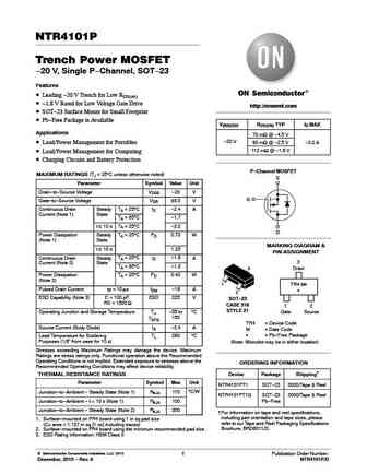
NTR4101P Trench Power MOSFET -20 V, Single P-Channel, SOT-23 Features Leading -20 V Trench for Low RDS(on) -1.8 V Rated for Low Voltage Gate Drive http //onsemi.com http //onsemi.com SOT-23 Surface Mount for Small Footprint Pb-Free Package is Available V(BR)DSS RDS(ON) TYP ID MAX Applications 70 mW @ -4.5 V -20 V Load/Power Management for Portables 90 mW @ -2.5
nths4101p.pdf
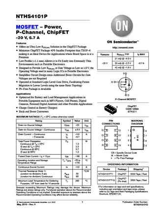
NTHS4101P MOSFET Power, P-Channel, ChipFET -20 V, 6.7 A Features Offers an Ultra Low RDS(on) Solution in the ChipFET Package http //onsemi.com Miniature ChipFET Package 40% Smaller Footprint than TSOP-6 making it an Ideal Device for Applications where Board Space is at a V(BR)DSS RDS(on) TYP ID MAX Premium 21 mW @ -4.5 V Low Profile (
fdd9410-f085.pdf
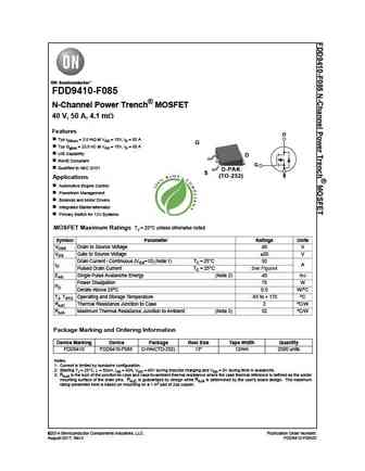
FDD9410-F085 N-Channel Power Trench MOSFET 40 V, 50 A, 4.1 m Features D Typ rDS(on) = 3.5 m at VGS = 10V, ID = 50 A G Typ Qg(tot) = 23.5 nC at VGS = 10V, ID = 50 A UIS Capability D RoHS Compliant G Qualified to AEC Q101 D-PAK TO-252 S S (TO-252) Applications Automotive Engine Control Powertrain Management Solenoid and Motor Drivers Integrated Starter/alt
ntr4101p ntrv4101p.pdf

NTR4101P, NTRV4101P Trench Power MOSFET -20 V, Single P-Channel, SOT-23 Features Leading -20 V Trench for Low RDS(on) -1.8 V Rated for Low Voltage Gate Drive www.onsemi.com www.onsemi.com SOT-23 Surface Mount for Small Footprint NTRV Prefix for Automotive and Other Applications Requiring Unique Site and Control Change Requirements; AEC-Q101 V(BR)DSS RDS(ON) TYP ID MAX
fdd9410l-f085.pdf
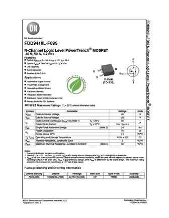
FDD9410L-F085 N-Channel Logic Level PowerTrench MOSFET 40 V, 50 A, 4.2 m Features D Typical RDS(on) = 3.3 m at VGS = 10V, ID = 50 A Typical Qg(tot) = 29 nC at VGS = 10V, ID = 50 A UIS Capability D RoHS Compliant G Qualified to AEC Q101 G S Applications D-PAK TO-252 Automotive Engine Control S (TO-252) PowerTrain Management Solenoid and Motor Drivers Elec
nvmfs5c410n.pdf
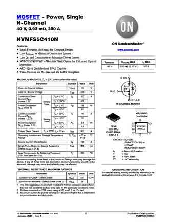
MOSFET - Power, Single N-Channel 40 V, 0.92 mW, 300 A NVMFS5C410N Features www.onsemi.com Small Footprint (5x6 mm) for Compact Design Low RDS(on) to Minimize Conduction Losses Low QG and Capacitance to Minimize Driver Losses NVMFS5C410NWF - Wettable Flank Option for Enhanced Optical V(BR)DSS RDS(ON) MAX ID MAX Inspection 40 V 0.92 mW @ 10 V 300 A AEC-Q101 Qualif
nthd4102p-d.pdf
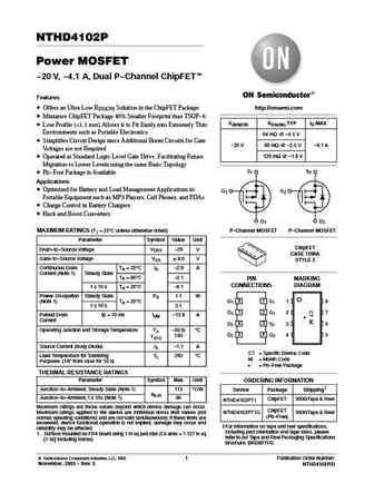
NTHD4102P Power MOSFET -20 V, -4.1 A, Dual P-Channel ChipFETt Features Offers an Ultra Low RDS(ON) Solution in the ChipFET Package http //onsemi.com Miniature ChipFET Package 40% Smaller Footprint than TSOP-6 V(BR)DSS RDS(ON) TYP ID MAX Low Profile (
nths4101pt1g.pdf
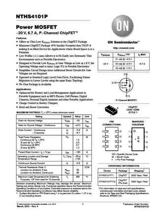
NTHS4101P Power MOSFET -20 V, 6.7 A, P-Channel ChipFETt Features Offers an Ultra Low RDS(on) Solution in the ChipFET Package Miniature ChipFET Package 40% Smaller Footprint than TSOP-6 http //onsemi.com making it an Ideal Device for Applications where Board Space is at a Premium V(BR)DSS RDS(on) TYP ID MAX Low Profile (
ntmfs5c410nlt.pdf
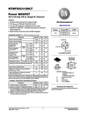
NTMFS5C410NLT Power MOSFET 40 V, 0.9 mW, 315 A, Single N-Channel Features Small Footprint (5x6 mm) for Compact Design Low RDS(on) to Minimize Conduction Losses www.onsemi.com Low QG and Capacitance to Minimize Driver Losses NTMFS5C410NLTWF - Wettable Flank Option for Enhanced Optical Inspection V(BR)DSS RDS(ON) MAX ID MAX These Devices are Pb-Free and are RoHS Com
ntms4101pr2.pdf
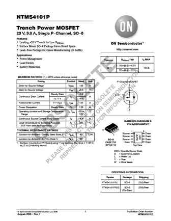
NTMS4101P Trench Power MOSFET 20 V, 9.0 A, Single P-Channel, SO-8 Features Leading -20 V Trench for Low RDS(on) Surface Mount SO-8 Package Saves Board Space http //onsemi.com Lead-Free Package for Green Manufacturing (G Suffix) Applications Power Management V(BR)DSS RDS(on) TYP ID MAX Load Switch 16 mW @ -4.5 V Battery Protection -20 V -9.0 A 22 mW @ -2.5
2sc4410.pdf
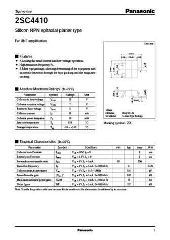
Transistor 2SC4410 Silicon NPN epitaxial planer type For UHF amplification Unit mm 2.1 0.1 Features 0.425 1.25 0.1 0.425 Allowing the small current and low voltage operation. High transition frequency fT. 1 S-Mini type package, allowing downsizing of the equipment and 3 automatic insertion through the tape packing and the magazine packing. 2 Absolute Maximum Ratings (Ta=25 C
mtm68410.pdf
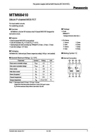
This product complies with the RoHS Directive (EU 2002/95/EC). MTM68410 Silicon P-channel MOS FET For load switch circuits For switching circuits Package Overview Code MTM68410 is the low ON resistance dual P-channel MOS FET designed for WMini8-F1 load switch circuits. Package dimension clicks here. Click! Features Pin Name Dual P-channel MOS FET in o
2sc4410 e.pdf

Transistor 2SC4410 Silicon NPN epitaxial planer type For UHF amplification Unit mm 2.1 0.1 Features 0.425 1.25 0.1 0.425 Allowing the small current and low voltage operation. High transition frequency fT. 1 S-Mini type package, allowing downsizing of the equipment and 3 automatic insertion through the tape packing and the magazine packing. 2 Absolute Maximum Ratings (Ta=25 C
vn2410.pdf
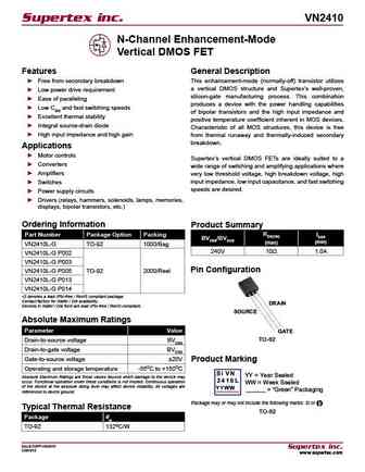
Supertex inc. VN2410 N-Channel Enhancement-Mode Vertical DMOS FET Features General Description Free from secondary breakdown This enhancement-mode (normally-off) transistor utilizes a vertical DMOS structure and Supertex s well-proven, Low power drive requirement silicon-gate manufacturing process. This combination Ease of paralleling produces a device with the power h
utd410.pdf
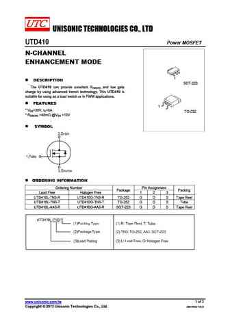
UNISONIC TECHNOLOGIES CO., LTD UTD410 Power MOSFET N-CHANNEL ENHANCEMENT MODE 1 DESCRIPTION SOT-223 The UTD410 can provide excellent RDS(ON) and low gate charge by using advanced trench technology. This UTD410 is suitable for using as a load switch or in PWM applications. FEATURES 1 * VDS=30V, ID=8A TO-252 * RDS(ON) =48m @VGS =10V SYMBOL ORDERING INFORMATI
ut4410.pdf
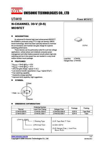
UNISONIC TECHNOLOGIES CO., LTD UT4410 Power MOSFET N-CHANNEL 30-V (D-S) MOSFET DESCRIPTION As advanced N-channel logic level enhancement MOSFET, the UT4410 is produced using UTC s high cell density, DMOS trench technology. which has been specially tailored to minimize the on-resistance and maintain low gate charge for superior switching performance. These devices can be
ut7410.pdf
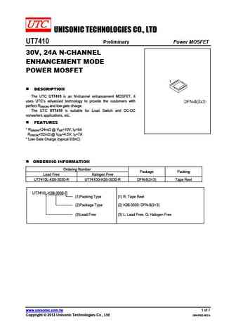
UNISONIC TECHNOLOGIES CO., LTD UT7410 Preliminary Power MOSFET 30V, 24A N-CHANNEL ENHANCEMENT MODE POWER MOSFET DESCRIPTION The UTC UT7410 is an N-channel enhancement MOSFET, it uses UTC s advanced technology to provide the customers with perfect RDS(ON) and low gate charge. The UTC UT7410 is suitable for Load Switch and DC-DC converters applications, etc. FEATURES
mcd3410.pdf
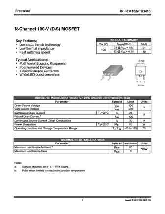
Freescale IRFR3410/ MCD3410 N-Channel 100-V (D-S) MOSFET PRODUCT SUMMARY Key Features rDS(on) (m ) VDS (V) ID(A) Low r trench technology DS(on) 78 @ VGS = 10V 21 Low thermal impedance 100 92 @ VGS = 4.5V 19 Fast switching speed Typical Applications PoE Power Sourcing Equipment PoE Powered Devices Telecom DC/DC converters White LED boost conve
itc14410.pdf
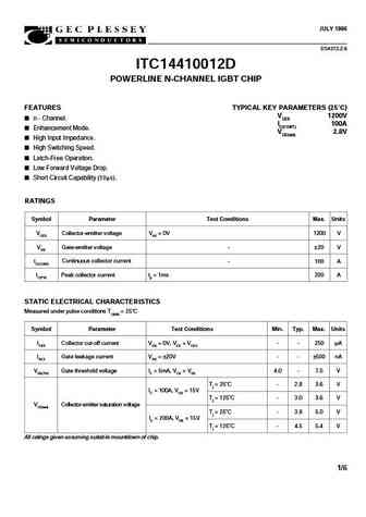
JULY 1996 IT14410012D PRELIMINARY DATA DS4372-2.6 ITC14410012D POWERLINE N-CHANNEL IGBT CHIP FEATURES TYPICAL KEY PARAMETERS (25 C) VCES 1200V n - Channel. IC(CONT) 100A Enhancement Mode. VCE(sat) 2.8V High Input Impedance. High Switching Speed. Latch-Free Operation. Low Forward Voltage Drop. Short Circuit Capability (10 s). RATINGS Symbol Parameter Test Conditions Ma
gf9410.pdf
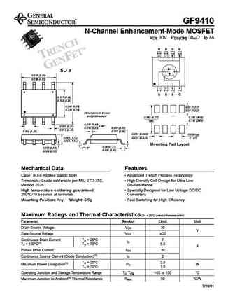
GF9410 N-Channel Enhancement-Mode MOSFET V 30V R 30 I 7A DS DS(ON) m D SO-8 0.197 (5.00) 0.189 (4.80) 8 5 0.157 (3.99) 0.150 (3.81) 0.244 (6.20) 0.05 (1.27) 0.228 (5.79) 0.04 (1.02) Dimensions in inches 1 4 and (millimeters) 0.245 (6.22) 0.165 (4.19) Min. 0.155 (3.94) 0.019 (0.48) x 45 0.020 (0.51) 0.010 (0.25) 0.009 (0.23) 0.013 (0.33) 0.050 (1.27) 0.007 (0.18)
2sk410.pdf
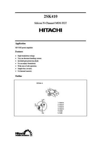
2SK410 Silicon N-Channel MOS FET Application HF/VHF power amplifier Features High breakdown voltage You can decrease handling current. Included gate protection diode No secondary breakdown Wide area of safe operation Simple bias circuitry No thermal runaway Outline 2SK410 Absolute Maximum Ratings (Ta = 25 C) Item Symbol Ratings Unit Drain to sourc
irfr410 irfu410.pdf

IRFR410, IRFU410 Data Sheet July 1999 File Number 3372.2 1.5A, 500V, 7.000 Ohm, N-Channel Power Features MOSFETs 1.5A, 500V These are N-Channel enhancement mode silicon gate rDS(ON) = 7.000 power field effect transistors. They are advanced power Single Pulse Avalanche Energy Rated MOSFETs designed, tested, and guaranteed to withstand a specified level of energy in the b
jansr2n7410.pdf
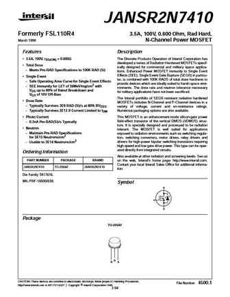
JANSR2N7410 Formerly FSL110R4 3.5A, 100V, 0.600 Ohm, Rad Hard, March 1998 N-Channel Power MOSFET Features Description 3.5A, 100V, rDS(ON) = 0.600 The Discrete Products Operation of Intersil Corporation has developed a series of Radiation Hardened MOSFETs specif- Total Dose ically designed for commercial and military space applica- - Meets Pre-RAD Specifications to 100K RAD (S
mg9410-r.pdf
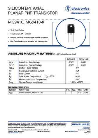
SILICON EPITAXIAL PLANAR PNP TRANSISTOR MG9410, MG9410-R TO-3P Plastic Package Complimentary NPN MG6330 Designed specifically for audio power amplifier applications High Current audio bipolar with wide Safe Operating Area ABSOLUTE MAXIMUM RATINGS (TA = 25 C unless otherwise stated) MG9410 MG9410-R VCBO Collector Base Voltage -230V -260V VCEO Col
2n4104.pdf
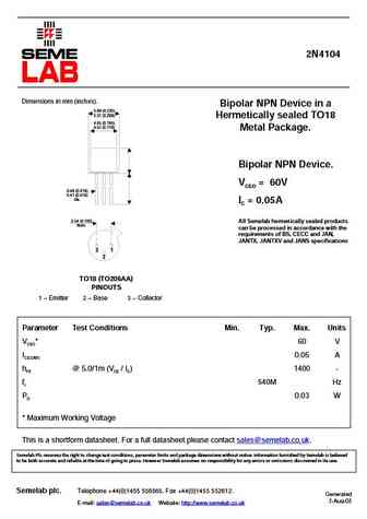
2N4104 Dimensions in mm (inches). Bipolar NPN Device in a 5.84 (0.230) 5.31 (0.209) Hermetically sealed TO18 4.95 (0.195) 4.52 (0.178) Metal Package. Bipolar NPN Device. VCEO = 60V 0.48 (0.019) 0.41 (0.016) dia. IC = 0.05A 2.54 (0.100) All Semelab hermetically sealed products Nom. can be processed in accordance with the requirements of BS, CECC and JAN, JANTX, JA
ssm0410.pdf
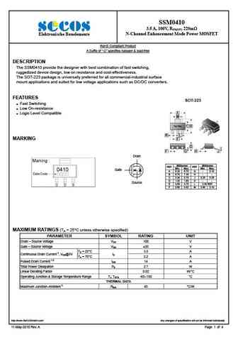
SSM0410 3.5 A, 100V, RDS(ON) 220m N-Channel Enhancement Mode Power MOSFET Elektronische Bauelemente RoHS Compliant Product A Suffix of -C specifies halogen & lead-free DESCRIPTION The SSM0410 provide the designer with best combination of fast switching, ruggedized device design, low on resistance and cost-effectiveness. The SOT-223 package is universally preferred for
sgm0410s.pdf
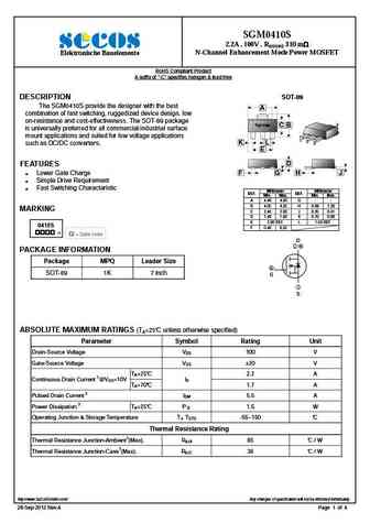
SGM0410S 2.2A , 100V , RDS(ON) 310 m N-Channel Enhancement Mode Power MOSFET Elektronische Bauelemente RoHS Compliant Product A suffix of -C specifies halogen & lead-free DESCRIPTION SOT-89 The SGM0410S provide the designer with the best A combination of fast switching, ruggedized device design, low on-resistance and cost-effectiveness. The SOT-89 pac
sgm0410.pdf
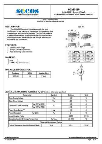
SGM0410 3.5A , 100V , RDS(ON) 170 m N-Channel Enhancement Mode Power MOSFET Elektronische Bauelemente RoHS Compliant Product A suffix of -C specifies halogen & lead-free DESCRIPTION SOT-89 The SGM0410 provide the designer with the best A combination of fast switching, ruggedized device design, low on-resistance and cost-effectiveness. The SOT-89 package 4 Top Vie
ssg4410n.pdf
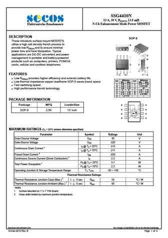
SSG4410N 13 A, 30 V, RDS(ON) 13.5 m N-Ch Enhancement Mode Power MOSFET Elektronische Bauelemente DESCRIPTION SOP-8 These miniature surface mount MOSFETs utilize a high cell density trench process to B provide low RDS(on) and to ensure minimal power loss and heat dissipation. Typical applications are DC-DC converters and power L D management in portable and battery-pow
ssg0410.pdf
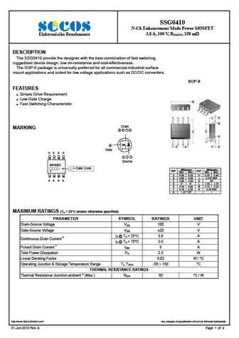
SSG0410 N-Ch Enhancement Mode Power MOSFET 3.8 A, 100 V, RDS(ON) 158 m Elektronische Bauelemente DESCRIPTION The SSG0410 provide the designer with the best combination of fast switching, ruggedized device design, low on-resistance and cost-effectiveness. The SOP-8 package is universally preferred for all commercial-industrial surface mount applications and suited for low volt
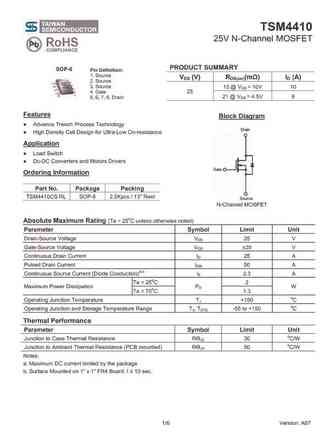
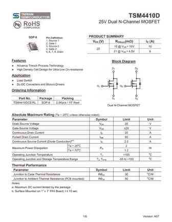
bd410.pdf
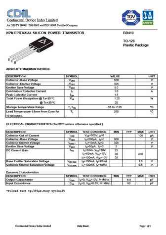
Continental Device India Limited An ISO/TS 16949, ISO 9001 and ISO 14001 Certified Company NPN EPITAXIAL SILICON POWER TRANSISTOR BD410 TO-126 Plastic Package E C B ABSOLUTE MAXIMUM RATINGS DESCRIPTION SYMBOL VALUE UNIT Collector -Base Voltage VCBO 500 V Collector -Emitter Voltage VCEO 325 V Emitter Base Voltage VEBO 5.0 V Continuous Collector Current IC 1.0 A Peak Collector Curr
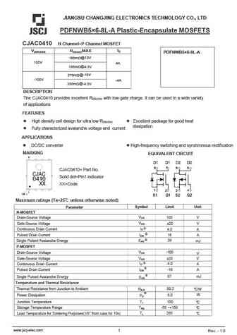
cjd4410.pdf
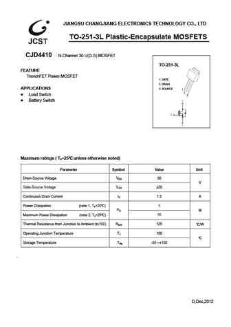
JIANGSU CHANGJIANG ELECTRONICS TECHNOLOGY CO., LTD TO-251-3L Plastic-Encapsulate MOSFETS CJD4410 N-Channel 30-V(D-S) MOSFET TO-2 51-3L FEATURE TrenchFET Power MOSFET 1. GATE 2. DRAIN APPLICATIONS 3. SOURCE Load Switch Battery Switch Maximum ratings ( Ta=25 unless otherwise noted) Parameter Symbol Value Unit Drain-Source Voltage VDS 30 V Gate-Source Voltage
cjq4410.pdf
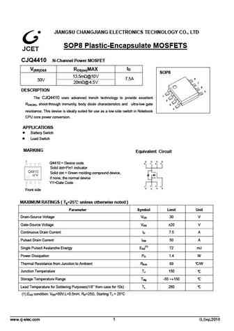
JIANGSU CHANGJIANG ELECTRONICS TECHNOLOGY CO., LTD SOP8 Plastic-Encapsulate MOSFETS CJQ4410 N-Channel Power MOSFET ID V(BR)DSS R DS(on) MAX SOP8 13.5 10 m @ V 7.5A 30V 20m @ 4.5V DESCRIPTION The CJQ4410 uses advanced trench technology to provide excellent RDS(ON), shoot-through immunity, body diode characteristics and ultra-low gate resistance. This device is ideall
krc410e-krc414e.pdf
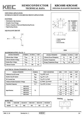
SEMICONDUCTOR KRC410E KRC414E EPITAXIAL PLANAR NPN TRANSISTOR TECHNICAL DATA SWITCHING APPLICATION. INTERFACE CIRCUIT AND DRIVER CIRCUIT APPLICATION. E FEATURES B DIM MILLIMETERS With Built-in Bias Resistors. _ + A 1.60 0.10 D Simplify Circuit Design. _ + 2 B 0.85 0.10 _ + C 0.70 0.10 Reduce a Quantity of Parts and Manufacturing Process. 3 1 D 0.27+0.10/-0.05 _
krc410-krc411-krc414.pdf
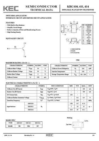
SEMICONDUCTOR KRC410, 411, 414 EPITAXIAL PLANAR NPN TRANSISTOR TECHNICAL DATA SWITCHING APPLICATION. INTERFACE CIRCUIT AND DRIVER CIRCUIT APPLICATION. E FEATURES M B M DIM MILLIMETERS With Built-in Bias Resistors. _ + A 2.00 0.20 D 2 _ Simplify Circuit Design. B 1.25 0.15 + _ + C 0.90 0.10 3 Reduce a Quantity of Parts and Manufacturing Process. 1 D 0.3+0.10/-0.05
krc410v-krc414v.pdf
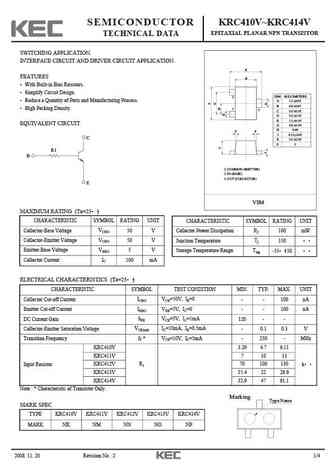
SEMICONDUCTOR KRC410V KRC414V EPITAXIAL PLANAR NPN TRANSISTOR TECHNICAL DATA SWITCHING APPLICATION. INTERFACE CIRCUIT AND DRIVER CIRCUIT APPLICATION. E FEATURES B With Built-in Bias Resistors. Simplify Circuit Design. DIM MILLIMETERS 2 _ Reduce a Quantity of Parts and Manufacturing Process. A 1.2 +0.05 _ B 0.8 +0.05 High Packing Density. 1 3 _ C 0.5 + 0.05 _ D 0.3
dki04103.pdf
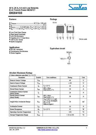
40 V, 29 A, 9.5 m Low RDS(ON) N ch Trench Power MOSFET DKI04103 Features Package TO-252 V(BR)DSS --------------------------------- 40 V (ID = 100 A) (4) ID ---------------------------------------------------------- 29 A D RDS(ON) -------- 11.8 m max. (VGS = 10 V, ID = 18.8 A) Qg ------- 5.1 nC (VGS = 4.5 V, VDS = 20 V, ID = 23.6 A) Low Total Gate
gki04101.pdf
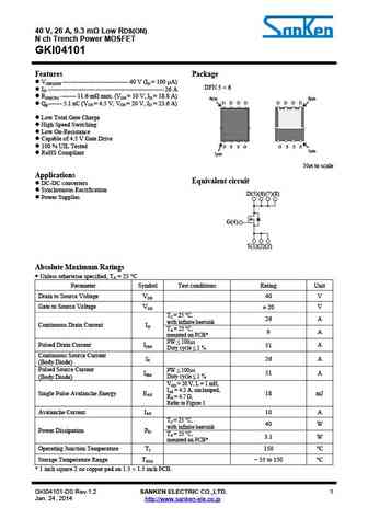
40 V, 26 A, 9.3 m Low RDS(ON) N ch Trench Power MOSFET GKI04101 Features Package V(BR)DSS --------------------------------- 40 V (ID = 100 A) DFN 5 6 ID ---------------------------------------------------------- 26 A RDS(ON) -------- 11.6 m max. (VGS = 10 V, ID = 18.8 A) 8pin 8pin D D D D D D D D Qg ------- 5.1 nC (VGS = 4.5 V, VDS = 20 V, ID = 23.


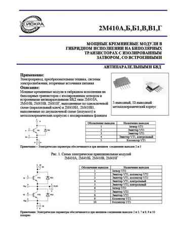
pt4410.pdf
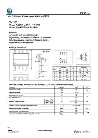
PT4410 30V N-Channel Enhancement Mode MOSFET VDS= 30V RDS(ON), Vgs@10V, Ids@12A = 10.5m RDS(ON), Vgs@4.5V, Ids@12A = 15m Features Advanced trench process technology High Density Cell Design For Ultra Low On-Resistance Fully Characterized Avalanche Voltage and Current Improved Shoot-Through FOM Package Dimensions D D D D 8 7 6 5 1 2 3 4 S S S G Millimeter Millimeter
2sc4102.pdf
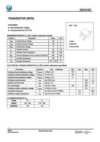
2SC4102 TRANSISTOR (NPN) FEATURES SOT 323 High Breakdown Voltage Complements the 2SA1579 MAXIMUM RATINGS (Ta=25 unless otherwise noted) Symbol Parameter Value Unit V Collector-Base Voltage 120 V CBO 1. BASE V Collector-Emitter Voltage 120 V 2. EMITTER CEO 3. COLLECTOR V Emitter-Base Voltage 5 V EBO I Collector Current 50 mA C P Collector Power Dissipat
cem0410.pdf
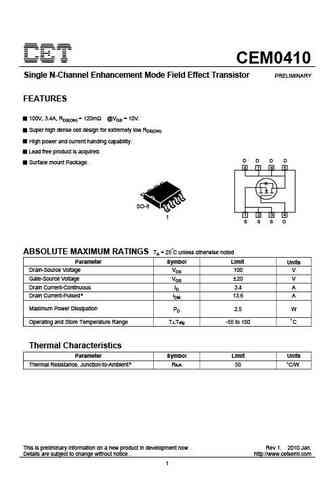
CEM0410 Single N-Channel Enhancement Mode Field Effect Transistor PRELIMINARY FEATURES 100V, 3.4A, RDS(ON) = 120m @VGS = 10V. Super high dense cell design for extremely low RDS(ON). High power and current handing capability. Lead free product is acquired. D D D D Surface mount Package. 8 7 6 5 SO-8 1 2 3 4 1 S S S G ABSOLUTE MAXIMUM RATINGS TA = 25 C unless otherwise noted Pa
wt4410m.pdf
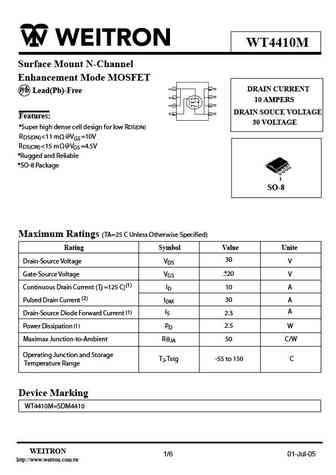
WT4410M Surface Mount N-Channel Enhancement Mode MOSFET DRAIN CURRENT P b Lead(Pb)-Free 10 AMPERS DRAIN SOUCE VOLTAGE Features 30 VOLTAGE *Super high dense cell design for low R DS(ON) RDS(ON)
wtk9410.pdf
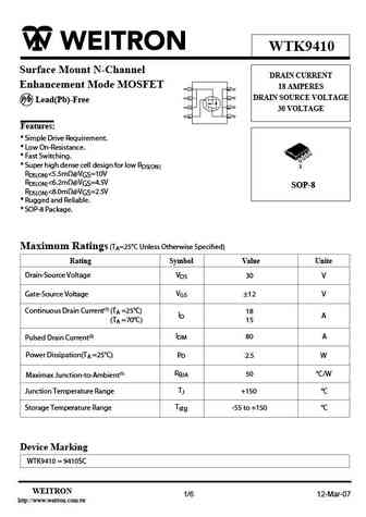
WTK9410 Surface Mount N-Channel DRAIN CURRENT Enhancement Mode MOSFET 18 AMPERES DRAIN SOURCE VOLTAGE P b Lead(Pb)-Free 30 VOLTAGE Features * Simple Drive Requirement. * Low On-Resistance. * Fast Switching. * Super high dense cell design for low RDS(ON) 1 RDS(ON)
aon7410.pdf

AON7410 30V N-Channel MOSFET General Description Features The AON7410 uses advanced trench technology and design VDS (V) = 30V to provide excellent RDS(ON) with low gate charge. This ID = 24A (VGS = 10V) device is suitable for use in DC - DC converters and Load RDS(ON)
aod410.pdf
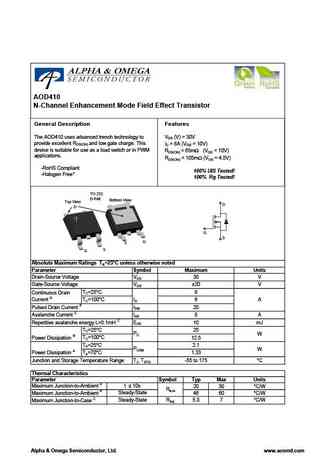
AOD410 N-Channel Enhancement Mode Field Effect Transistor General Description Features The AOD410 uses advanced trench technology to VDS (V) = 30V provide excellent RDS(ON) and low gate charge. This ID = 8A (VGS = 10V) device is suitable for use as a load switch or in PWM RDS(ON)
ao4410.pdf
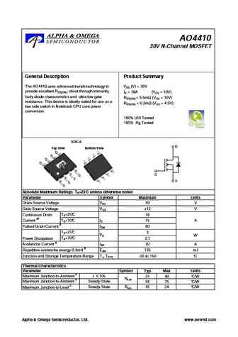
AO4410 30V N-Channel MOSFET General Description Product Summary The AO4410 uses advanced trench technology to VDS (V) = 30V provide excellent RDS(ON), shoot-through immunity, ID = 18A (VGS = 10V) body diode characteristics and ultra-low gate RDS(ON)
aod4102.pdf

AOD4102/AOI4102 30V N-Channel MOSFET General Description Product Summary VDS 30V The AOD4102/AOI4102 uses advanced trench technology and design to provide excellent RDS(ON) with ID (at VGS=10V) 19A low gate charge. This device is suitable for use in PWM, RDS(ON) (at VGS=10V)
aoca24108e.pdf
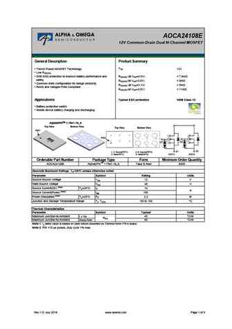
AOCA24108E 12V Common-Drain Dual N-Channel MOSFET General Description Product Summary VSS Trench Power MOSFET Technology 12V Low RSS(ON) With ESD protection to improve battery performance and RSS(ON) (at VGS=4.5V)
aon6410.pdf
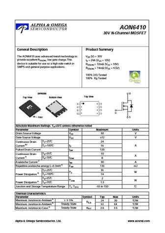
AON6410 30V N-Channel MOSFET General Description Product Summary The AON6410 uses advanced trench technology to VDS (V) = 30V provide excellent RDS(ON), low gate charge.This ID = 24A (VGS = 10V) device is suitable for use as a high side switch in RDS(ON)
aod4100.pdf
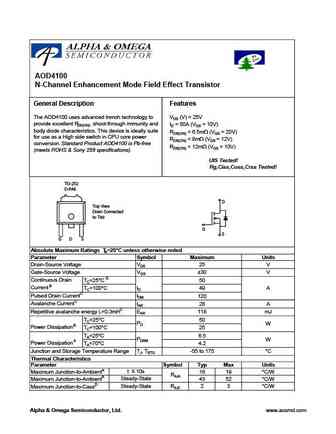
AOD4100 N-Channel Enhancement Mode Field Effect Transistor General Description Features The AOD4100 uses advanced trench technology to VDS (V) = 25V provide excellent RDS(ON), shoot-through immunity and ID = 50A (VGS = 10V) body diode characteristics. This device is ideally suite RDS(ON)
aow410.pdf
AOW410 100V N-Channel MOSFET TM SDMOS General Description Product Summary VDS 100V The AOW410 is fabricated with SDMOSTM trench 150A technology that combines excellent RDS(ON) with low gate ID (at VGS=10V) charge & low Qrr.The result is outstanding efficiency with
aon2410.pdf
AON2410 30V N-Channel MOSFET General Description Product Summary VDS The AON2410 combines advanced trench MOSFET 30V technology with a low resistance package to provide ID (at VGS=4.5V) 8A extremely low RDS(ON). This device is ideal for load switch RDS(ON) (at VGS = 4.5V)
aoca24106c.pdf
AOCA24106C 12V Common-Drain Dual N-Channel MOSFET General Description Product Summary VSS Trench Power MOSFET Technology 12V Ultra low RSS(ON) With ESD protection to improve battery performance and RSS(ON) (at VGS=4.5V)
ao7410.pdf
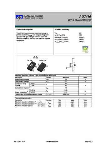
AO7410 30V N-Channel MOSFET General Description Product Summary VDS 30V The AO7410 uses advanced trench technology to provide excellent RDS(ON), very low gate charge and ID (at VGS=10V) 1.7A operation with gate voltages as low as 2.5V. This RDS(ON) (at VGS=10V)
aoe66410.pdf
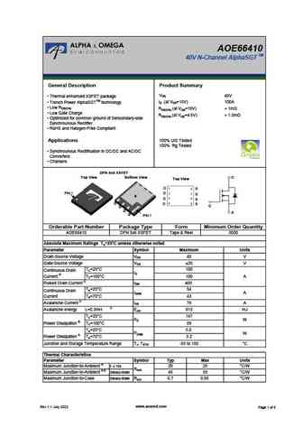
AOE66410 TM 40V N-Channel AlphaSGT General Description Product Summary VDS 40V Thermal enhanced XSFET package ID (at VGS=10V) 100A Trench Power AlphaSGTTM technology Low RDS(ON) RDS(ON) (at VGS=10V)
aoi4102.pdf
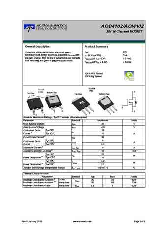
AOD4102/AOI4102 30V N-Channel MOSFET General Description Product Summary VDS 30V The AOD4102/AOI4102 uses advanced trench technology and design to provide excellent RDS(ON) with ID (at VGS=10V) 19A low gate charge. This device is suitable for use in PWM, RDS(ON) (at VGS=10V)
aot410l.pdf
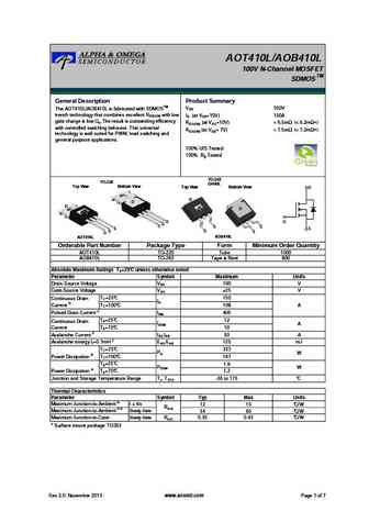
AOT410L/AOB410L 100V N-Channel MOSFET TM SDMOS General Description Product Summary 100V The AOT410L/AOB410L is fabricated with SDMOSTM VDS trench technology that combines excellent RDS(ON) with low ID (at VGS=10V) 150A gate charge & low Qrr.The result is outstanding efficiency RDS(ON) (at VGS=10V)
aob410l.pdf

AOT410L/AOB410L 100V N-Channel MOSFET TM SDMOS General Description Product Summary 100V The AOT410L/AOB410L is fabricated with SDMOSTM VDS trench technology that combines excellent RDS(ON) with low ID (at VGS=10V) 150A gate charge & low Qrr.The result is outstanding efficiency RDS(ON) (at VGS=10V)
aod4104.pdf
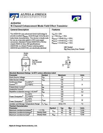
AOD4104 N-Channel Enhancement Mode Field Effect Transistor General Description Features The AOD4104 uses advanced trench technology to VDS (V) = 25V provide excellent RDS(ON), shoot-through immunity and ID = 75A (VGS = 10V) body diode characteristics. This device is ideally suite RDS(ON)
aod4106.pdf
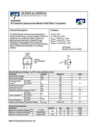
AOD4106 N-Channel Enhancement Mode Field Effect Transistor General Description Features The AOD4106 uses advanced trench technology to VDS (V) = 25V provide excellent RDS(ON), low gate charge.This device is ID = 50A (VGS = 20V) suitable for use as a low side switch in SMPS and RDS(ON)
aoca24106e.pdf
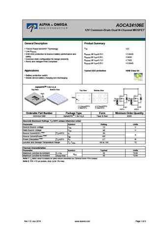
AOCA24106E 12V Common-Drain Dual N-Channel MOSFET General Description Product Summary VSS Trench Power MOSFET Technology 12V Low RSS(ON) With ESD protection to improve battery performance and RSS(ON) (at VGS=4.5V)
ap9410gh.pdf
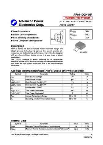
AP9410GH-HF Halogen-Free Product Advanced Power N-CHANNEL ENHANCEMENT MODE Electronics Corp. POWER MOSFET Low On-resistance D BVDSS 30V Simple Drive Requirement RDS(ON) 6m Fast Switching Characteristic ID 75A G RoHS Compliant & Halogen-Free S Description AP9410 series are from Advanced Power innovated design and G D silicon process technology to achieve the lowes
ap9410agm.pdf
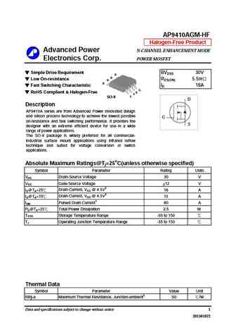
AP9410AGM-HF Halogen-Free Product Advanced Power N-CHANNEL ENHANCEMENT MODE Electronics Corp. POWER MOSFET Simple Drive Requirement BVDSS 30V D D Low On-resistance RDS(ON) 5.5m D D Fast Switching Characteristic ID 18A G RoHS Compliant & Halogen-Free S S S SO-8 D Description AP9410A series are from
ap9410gmt-hf.pdf
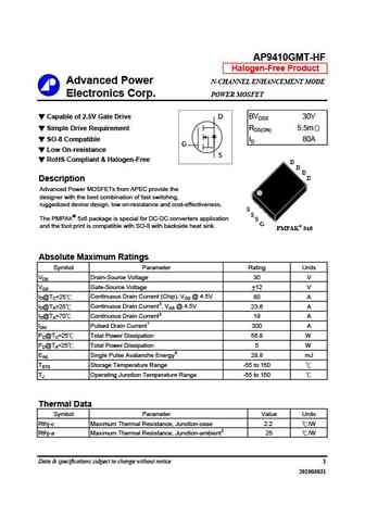
AP9410GMT-HF Halogen-Free Product Advanced Power N-CHANNEL ENHANCEMENT MODE Electronics Corp. POWER MOSFET Capable of 2.5V Gate Drive D BVDSS 30V Simple Drive Requirement RDS(ON) 5.5m SO-8 Compatible ID 80A G Low On-resistance S RoHS Compliant & Halogen-Free D D D D Description Advanced Power MOSFETs from APEC provide the designer with the best combina
ap4410m.pdf
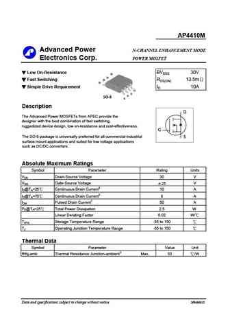
AP4410M Advanced Power N-CHANNEL ENHANCEMENT MODE Electronics Corp. POWER MOSFET Low On-Resistance BVDSS 30V D D Fast Switching D RDS(ON) 13.5m D Simple Drive Requirement ID 10A G S S SO-8 S Description D D The Advanced Power MOSFETs from APEC provide the designer with the best combination of fast switching, rugged
ap9410gm-hf.pdf
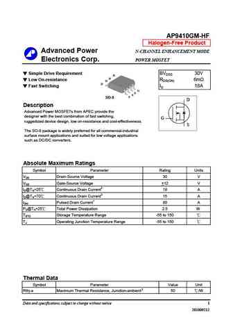
AP9410GM-HF Halogen-Free Product Advanced Power N-CHANNEL ENHANCEMENT MODE Electronics Corp. POWER MOSFET Simple Drive Requirement BVDSS 30V D D Low On-resistance RDS(ON) 6m D D Fast Switching ID 18A G S S S SO-8 D Description Advanced Power MOSFETs from APEC provide the designer with the best combination of fast switching, G ruggedized device design, low on-
ap4410agm.pdf
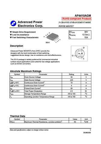
AP4410AGM RoHS-compliant Product Advanced Power N-CHANNEL ENHANCEMENT MODE Electronics Corp. POWER MOSFET Simple Drive Requirement BVDSS 30V D D Low On-resistance RDS(ON) 13.5m D D Fast Switching Characteristic ID 10A G S S S SO-8 Description D Advanced Power MOSFETs from APEC provide the designer with the best combination of fast switching, ruggedized device d
ap4410agm-hf.pdf
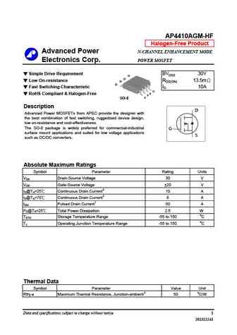
AP4410AGM-HF Halogen-Free Product Advanced Power N-CHANNEL ENHANCEMENT MODE Electronics Corp. POWER MOSFET Simple Drive Requirement BVDSS 30V D D Low On-resistance RDS(ON) 13.5m D D Fast Switching Characteristic ID 10A G S RoHS Compliant & Halogen-Free S S SO-8 Description D Advanced Power MOSFETs from APEC provide the designer with the best combination of
ap9410gm.pdf
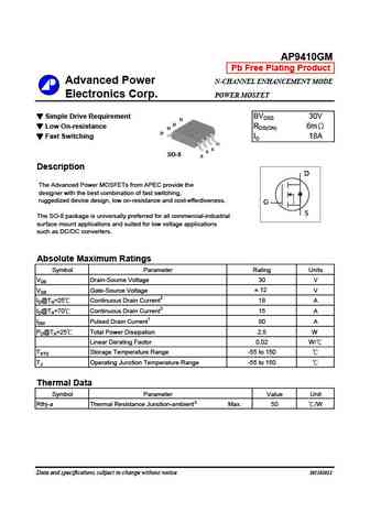
AP9410GM Pb Free Plating Product Advanced Power N-CHANNEL ENHANCEMENT MODE Electronics Corp. POWER MOSFET Simple Drive Requirement BVDSS 30V D D Low On-resistance RDS(ON) 6m D D Fast Switching ID 18A G S S SO-8 S Description D The Advanced Power MOSFETs from APEC provide the designer with the best combination of fa
ap9410gh-hf.pdf
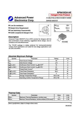
AP9410GH-HF Halogen-Free Product Advanced Power N-CHANNEL ENHANCEMENT MODE Electronics Corp. POWER MOSFET Low On-resistance D BVDSS 30V Simple Drive Requirement RDS(ON) 6m Fast Switching Characteristic ID 75A G RoHS Compliant & Halogen-Free S Description Advanced Power MOSFETs from APEC provide the designer with the G D best combination of fast switching, ruggedi
ap4410gm.pdf
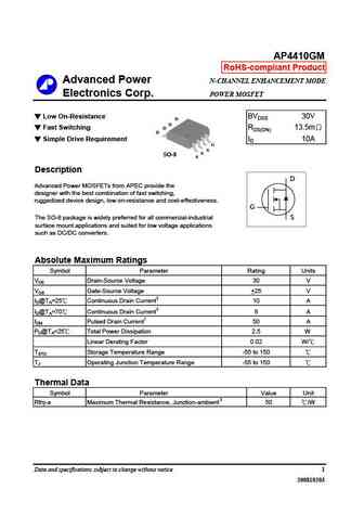
AP4410GM RoHS-compliant Product Advanced Power N-CHANNEL ENHANCEMENT MODE Electronics Corp. POWER MOSFET Low On-Resistance BVDSS 30V D D Fast Switching D RDS(ON) 13.5m D Simple Drive Requirement ID 10A G S S SO-8 S Description D D Advanced Power MOSFETs from APEC provide the designer with the best combination of fast switching, ruggedized device design, low on-
ap9410agh-hf.pdf
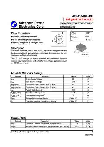
AP9410AGH-HF Halogen-Free Product Advanced Power N-CHANNEL ENHANCEMENT MODE Electronics Corp. POWER MOSFET Low On-resistance D BVDSS 30V Simple Drive Requirement RDS(ON) 6m Fast Switching Characteristic ID 67A G RoHS Compliant & Halogen-Free S Description Advanced Power MOSFETs from APEC provide the designer with the G D best combination of fast switching, rugged
ap9410agm-hf.pdf
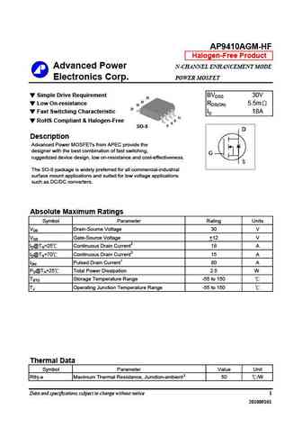
AP9410AGM-HF Halogen-Free Product Advanced Power N-CHANNEL ENHANCEMENT MODE Electronics Corp. POWER MOSFET Simple Drive Requirement BVDSS 30V D D Low On-resistance RDS(ON) 5.5m D D Fast Switching Characteristic ID 18A G RoHS Compliant & Halogen-Free S S S SO-8 D Description Advanced Power MOSFETs from APEC provide the designer with the best combination of fa
ap9410agh.pdf
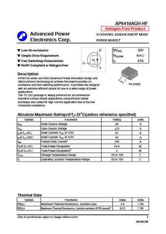
AP9410AGH-HF Halogen-Free Product Advanced Power N-CHANNEL ENHANCEMENT MODE Electronics Corp. POWER MOSFET Low On-resistance D BVDSS 30V Simple Drive Requirement RDS(ON) 6m Fast Switching Characteristic ID 67A G RoHS Compliant & Halogen-Free S Description AP9410A series are from Advanced Power innovated d
ama410n.pdf
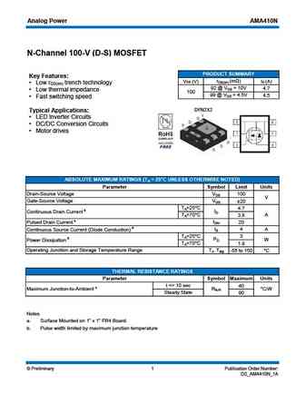
Analog Power AMA410N N-Channel 100-V (D-S) MOSFET PRODUCT SUMMARY Key Features rDS(on) (m ) VDS (V) ID (A) Low r trench technology DS(on) 92 @ VGS = 10V 4.7 Low thermal impedance 100 99 @ VGS = 4.5V 4.5 Fast switching speed DFN2X2 Typical Applications LED Inverter Circuits DC/DC Conversion Circuits Motor drives ABSOLUTE MAXIMUM RATINGS (TA
am7410n.pdf
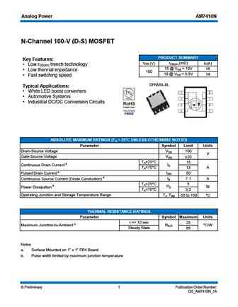
Analog Power AM7410N N-Channel 100-V (D-S) MOSFET PRODUCT SUMMARY Key Features rDS(on) (m ) VDS (V) ID(A) Low r trench technology DS(on) 15 @ VGS = 10V 15 Low thermal impedance 100 19 @ VGS = 5.5V 14 Fast switching speed DFN5X6-8L Typical Applications White LED boost converters Automotive Systems Industrial DC/DC Conversion Circuits ABSOLU
am9410n.pdf
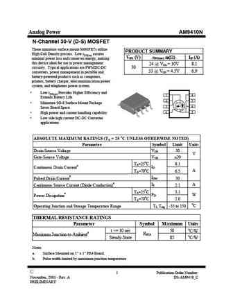
Analog Power AM9410N N-Channel 30-V (D-S) MOSFET These miniature surface mount MOSFETs utilize PRODUCT SUMMARY High Cell Density process. Low rDS(on) assures VDS (V) rDS(on) m( ) ID (A) minimal power loss and conserves energy, making this device ideal for use in power management 24 @ VGS = 10V 8.1 circuitry. Typical applications are PWMDC-DC 30 33 @ VGS = 4.5V 6.9 converters, p
am4410n.pdf
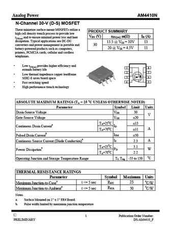
Analog Power AM4410N N-Channel 30-V (D-S) MOSFET These miniature surface mount MOSFETs utilize a PRODUCT SUMMARY high cell density trench process to provide low VDS (V) rDS(on) m( ) ID (A) rDS(on) and to ensure minimal power loss and heat dissipation. Typical applications are DC-DC 13.5 @ VGS = 10V 13 converters and power management in portable and 30 20 @ VGS = 4.5V 11 battery
afn4102w.pdf
AFN4102W Alfa-MOS 100V N-Channel Technology Enhancement Mode MOSFET General Description Features AFN4102W, N-Channel enhancement mode 100V/3.8A,RDS(ON)=158m @VGS=10V MOSFET, uses Advanced Trench Technology 100V/3.0A,RDS(ON)=175m @VGS=4.5V to provide excellent RDS(ON), low gate charge. Super high density cell design for extremely These devices are particularly suit
afn3410.pdf
AFN3410 Alfa-MOS 30V N-Channel Technology Enhancement Mode MOSFET General Description Features AFN3410, N-Channel enhancement mode 30V/6.0A,RDS(ON)=27m @VGS=10V MOSFET, uses Advanced Trench Technology 30V/4.5A,RDS(ON)=30m @VGS=4.5V to provide excellent RDS(ON), low gate charge. Super high density cell design for extremely These devices are particularly suited for
4410.pdf
Shenzhen Tuofeng Semiconductor Technology co., LTD 4410 N-Channel Enhancement-Mode MOSFET (30V, 10A) PRODUCT SUMMARY VDSS ID RDS(on) (m-ohm) Max 13.5 @ VGS = 10V ,ID=10A 30V 10A 20 @ VGS = 4.5V,ID=5A Features Advanced Trench Process Technology High Density Cell Design for Ultra Low On-Resistance Lead free product is acquired Surface mount Package Pin 1 /
ao3410.pdf
Shenzhen Tuofeng Semiconductor Technology Co., Ltd AO3410 AO3410 N-Channel Enhancement Mode Field Effect Transistor General Description Features The AO3410 uses advanced trench technology to VDS (V) = 30V provide excellent RDS(ON), low gate charge and ID = 5.0 A operation with gate voltages as low as 1.8V and as RDS(ON)
mtn4410v8.pdf
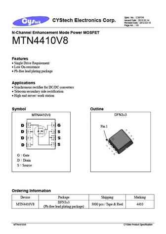
Spec. No. C397V8 Issued Date 2012.03.14 CYStech Electronics Corp. Revised Date 2012.03.15 Page No. 1/9 N-Channel Enhancement Mode Power MOSFET MTN4410V8 Features Single Drive Requirement Low On-resistance Pb-free lead plating package Applications Synchronous rectifier for DC/DC converters Telecom secondary side rectification High end s
mtn0410l3.pdf
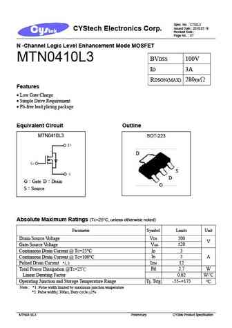
Spec. No. C792L3 Issued Date 2010.07.16 CYStech Electronics Corp. Revised Date Page No. 1/7 N -Channel Logic Level Enhancement Mode MOSFET BVDSS 100V MTN0410L3 ID 3A 280m RDSON(MAX) Features Low Gate Charge Simple Drive Requirement Pb-free lead plating package Equivalent Circuit Outline MTN0410L3 SOT-223 D S D G Gate D Drain G
mtn3410j3.pdf
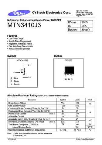
Spec. No. C433J3 Issued Date 2008.12.24 CYStech Electronics Corp. Revised Date 2010.07.22 Page No. 1/7 N-Channel Enhancement Mode Power MOSFET BVDSS 100V ID 50A MTN3410J3 RDS(ON) 30m Features Low Gate Charge Simple Drive Requirement Repetitive Avalanche Rated Fast Switching Characteristic RoHS compliant package Symbol Outline MTN3410
mtn3410f3.pdf
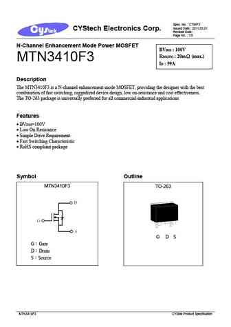
Spec. No. C795F3 Issued Date 2011.03.01 CYStech Electronics Corp. Revised Date Page No. 1/8 N-Channel Enhancement Mode Power MOSFET BVDSS 100V RDS(ON) 20m (max.) MTN3410F3 ID 59A Description The MTN3410F3 is a N-channel enhancement-mode MOSFET, providing the designer with the best combination of fast switching, ruggedized device design, low on-resistance a
mtn4410q8.pdf
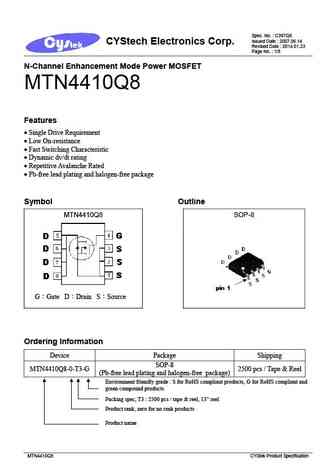
Spec. No. C397Q8 Issued Date 2007.06.14 CYStech Electronics Corp. Revised Date 2014.01.23 Page No. 1/8 N-Channel Enhancement Mode Power MOSFET MTN4410Q8 Features Single Drive Requirement Low On-resistance Fast Switching Characteristic Dynamic dv/dt rating Repetitive Avalanche Rated Pb-free lead plating and halogen-free package Symbol O
apm9410k.pdf
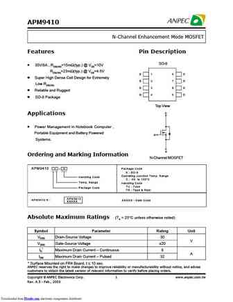
APM9410 N-Channel Enhancement Mode MOSFET Features Pin Description SO-8 30V/8A , RDS(ON)=15m (typ.) @ VGS=10V RDS(ON)=23m (typ.) @ VGS=4.5V S 1 8 D Super High Dense Cell Design for Extremely S 2 7 D Low RDS(ON) S 3 6 D Reliable and Rugged G 45 D SO-8 Package Top View D Applications Power Managem
apm4410.pdf
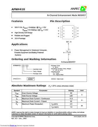
APM4410 N-Channel Enhancement Mode MOSFET Features Pin Description 30V/11.5A, RDS(ON) = 9m (typ.) @ VGS = 10V S 1 8 D RDS(ON) =14.5m (typ.) @ VGS = 4.5V S 2 7 D High Density Cell Design S 3 6 D Reliable and Rugged G 45 D SO-8 Package SO - 8 D Applications Power Management in Notebook Computer, G
apm4101k.pdf
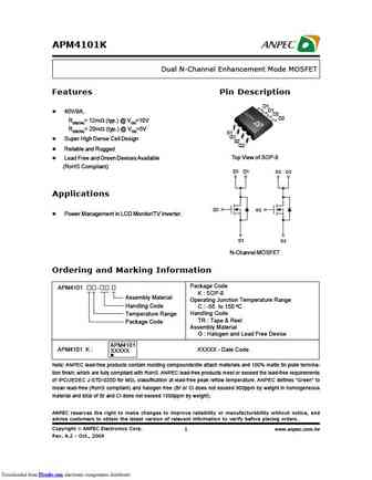
APM4101K Dual N-Channel Enhancement Mode MOSFET Features Pin Description D1 D1 40V/9A, D2 D2 RDS(ON)= 12m (typ.) @ VGS=10V RDS(ON)= 20m (typ.) @ VGS=5V S1 G1 Super High Dense Cell Design S2 G2 Reliable and Rugged Top View of SOP-8 Lead Free and Green Devices Available (RoHS Compliant) D1 D1 D2 D2 Applications G1 G2 Power Management in LCD Monitor/TV Inverter.
apm9410.pdf
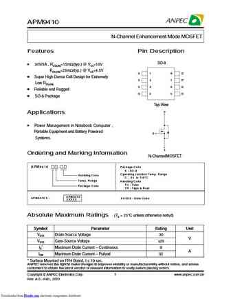
APM9410 N-Channel Enhancement Mode MOSFET Features Pin Description SO-8 30V/8A , RDS(ON)=15m (typ.) @ VGS=10V RDS(ON)=23m (typ.) @ VGS=4.5V S 1 8 D Super High Dense Cell Design for Extremely S 2 7 D Low RDS(ON) S 3 6 D Reliable and Rugged G 45 D SO-8 Package Top View D Applications Power Managem
stu410s std410s.pdf
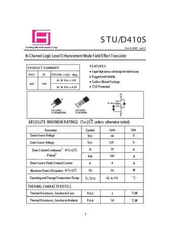
S TU/D410S S amHop Microelectronics C orp. ver1.1 Oct. 9, 2007 N-Channel Logic Level E nhancement Mode Field E ffect Transistor FEATUR ES PR ODUCT S UMMAR Y S uper high dense cell design for low R DS (ON). VDS S ID R DS (ON) ( m ) Max R ugged and reliable. 20 @ VGS = 10V Surface Mount Package. 30A 40V ESD Protected. 30 @ VGS =4.5V D D D G G G S S STU SERIES STD SERIE
stm4410a.pdf
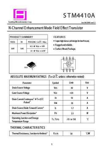
S T M4410A S amHop Microelectronics C orp. J an 04 2005 ver1.1 N-C hannel E nhancement Mode Field E ffect Transistor P R ODUC T S UMMAR Y F E AT UR E S S uper high dense cell design for low R DS (ON). V DS S ID R DS (ON) ( m W ) Max R ugged and reliable. 9.5 @ V G S = 10V 30V 10A S urface Mount Package. 21 @ V G S = 4.5V S O-8 1 ABS OLUTE MAXIMUM R ATINGS (TA=25 C unless other
sdm4410.pdf
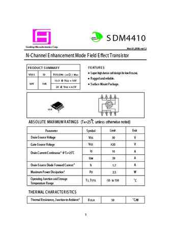
Green Product S DM4410 S amHop Microelectronics C orp. Mar.01,2006 ver1.2 N-Channel E nhancement Mode Field E ffect Transistor PR ODUC T S UMMAR Y F E ATUR E S S uper high dense cell design for low R DS (ON). VDS S ID R DS (ON) ( m ) Max R ugged and reliable. 13.5 @ VG S = 10V 30V 10A S urface Mount Package. 20 @ VG S = 4.5V S O-8 1 ABS OLUTE MAXIMUM R ATINGS (TA=25 C unless
stb4410 stp4410.pdf
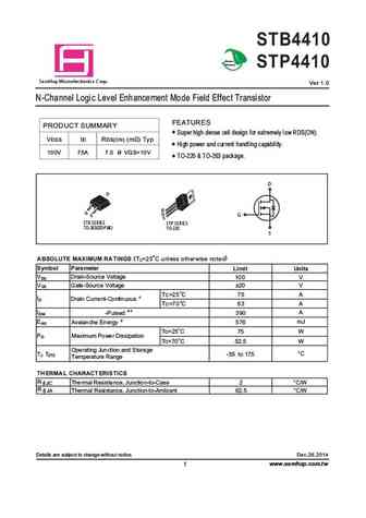
STB4410 Green Product STP4410 a S mHop Microelectronics C orp. Ver 1.0 N-Channel Logic Level Enhancement Mode Field Effect Transistor FEATURES PRODUCT SUMMARY Super high dense cell design for extremely low RDS(ON). VDSS ID RDS(ON) (m ) Typ High power and current handling capability. 100V 75A 7.0 @ VGS=10V TO-220 & TO-263 package. D G STB SERIES STP SERIES TO-263(DD-PAK) TO-
pa410bd.pdf
PA410BD N-Channel Enhancement Mode MOSFET PRODUCT SUMMARY V(BR)DSS RDS(ON) ID 140m @VGS = 10V 100V 10A TO-252 ABSOLUTE MAXIMUM RATINGS (TA = 25 C Unless Otherwise Noted) PARAMETERS/TEST CONDITIONS SYMBOL LIMITS UNITS VDS Drain-Source Voltage 100 V VGS Gate-Source Voltage 20 V TC = 25 C 10 ID Continuous Drain Current TC = 100 C 7 A IDM 30 Pulsed Drain Curren
lp4101lt1g.pdf
LESHAN RADIO COMPANY, LTD. 20V P-Channel Enhancement-Mode MOSFET LP4101LT1G V = -20V DS R Vgs@-4.5V, Ids@-2.8A = 100 m DS(ON), m RDS(ON), Vgs@-2.5V, Ids@-2.0A = 150 3 Features Advanced trench process technology 1 High Density Cell Design For Ultra Low On-Resistance 2 Fully Characterized Avalanche Voltage and Current SOT 23 (TO 236AB) Improved Shoot-Through FOM
lp4101lt1g s-lp4101lt1g.pdf
LESHAN RADIO COMPANY, LTD. 20V P-Channel Enhancement-Mode MOSFET V = -20V DS LP4101LT1G R Vgs@-4.5V, Ids@-2.8A = 100 m DS(ON), S-LP4101LT1G m RDS(ON), Vgs@-2.5V, Ids@-2.0A = 150 Features 3 Advanced trench process technology High Density Cell Design For Ultra Low On-Resistance 1 Fully Characterized Avalanche Voltage and Current Improved Shoot-Through FOM 2 we declar
irf4410a irf4410h.pdf
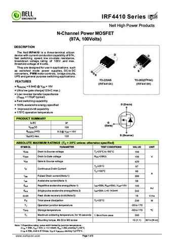
RoHS IRF4410 Series RoHS SEMICONDUCTOR Nell High Power Products N-Channel Power MOSFET (97A, 100Volts) DESCRIPTION The Nell IRF4410 is a three-terminal silicon D device with current conduction capability of 97A, D fast switching speed, low on-state resistance, breakdown voltage rating of 100V ,and max. threshold voltage of 4 volts. G They are designed for use in application
hc4106.pdf
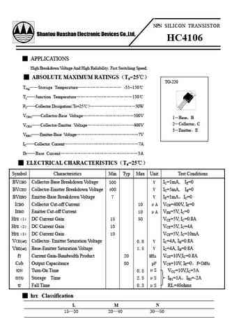
NPN S I L I C O N T R A N S I S T O R Shantou Huashan Electronic Devices Co.,Ltd. HC4106 APPLICATIONS High Breakdown Voltage And High Reliability.Fast Switching Speed. ABSOLUTE MAXIMUM RATINGS Ta=25 TO-220 Tstg Storage Temperature -55 150 Tj Junction Temperature 150 PC Collec
cs3410 b4.pdf
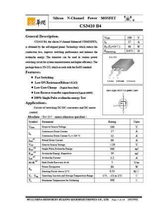
Silicon N-Channel Power MOSFET R CS3410 B4 General Description VDSS 100 V CS3410 B4, the silicon N-channel Enhanced VDMOSFETs, ID 17 A PD (TC=25 ) 80 W is obtained by the self-aligned planar Technology which reduce the RDS(ON)Typ 0.075 conduction loss, improve switching performance and enhance the avalanche energy. The transistor can be used in various power
cs3410 br.pdf
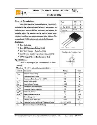
Silicon N-Channel Power MOSFET R CS3410 BR General Description VDSS 100 V CS3410 BR, the silicon N-channel Enhanced VDMOSFETs, ID 17 A PD (TC=25 ) 80 W is obtained by the self-aligned planar Technology which reduce the RDS(ON)Typ 0.075 conduction loss, improve switching performance and enhance the avalanche energy. The transistor can be used in various power
cs3410 b3.pdf
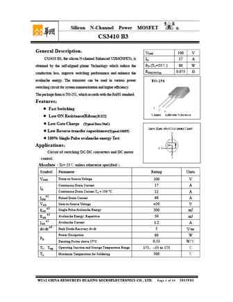
Silicon N-Channel Power MOSFET R CS3410 B3 General Description VDSS 100 V CS3410 B3, the silicon N-channel Enhanced VDMOSFETs, is ID 17 A PD (TC=25 ) 80 W obtained by the self-aligned planar Technology which reduce the RDS(ON)Typ 0.075 conduction loss, improve switching performance and enhance the avalanche energy. The transistor can be used in various power
cs5410.pdf
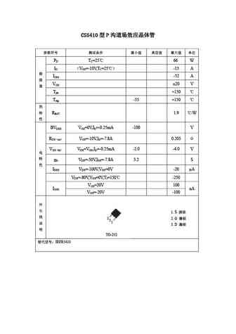
CS5410 P PD TC=25 66 W ID VGS=-10V,TC=25 -13 A IDM -52 A VGS 20 V Tjm +150 Tstg -55 +150 RthJC 1.9 /W BVDSS VGS=0V,ID=-0.25mA -100 V RDS on VGS=-10V,ID=-7.8A 0.205 VGS th VDS=VGS,ID=-0.25mA -2.0 -4.0 V gfs
csr3410.pdf
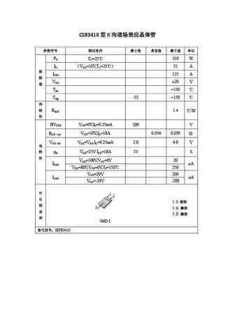
CSR3410 N PD TC=25 110 W ID VGS=10V,TC=25 31 A IDM 125 A VGS 20 V Tjm +150 Tstg -55 +150 RthJC 1.4 /W BVDSS VGS=0V,ID=0.25mA 100 V RDS on VGS=10V,ID=18A 0.034 0.039 VGS th VDS=VGS,ID=0.25mA 2.0 4.0 V
ntr4101p ntrv4101p.pdf
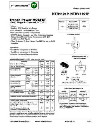
Product specification NTR4101P, NTRV4101P Trench Power MOSFET V(BR)DSS RDS(ON) TYP ID MAX -20 V, Single P-Channel, SOT-23 70 mW @ -4.5 V Features -20 V 90 mW @ -2.5 V -3.2 A Leading -20 V Trench for Low RDS(on) 112 mW @ -1.8 V -1.8 V Rated for Low Voltage Gate Drive SOT-23 Surface Mount for Small Footprint P-Channel MOSFET NTRV Prefix for Automotive and Other Applic
ftk4410d.pdf
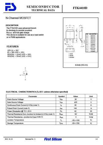
SEMICONDUCTOR FTK4410D TECHNICAL DATA N-Channel MOSFET A I DESCRIPTION C J The FTK410D uses advanced trench te chnology to provide excellent RDS(ON) and low gate charge. DIM MILLIMETERS This device is suitable for use as a load switch A 6 50 0 2 B 5 60 0 2 or in PWM applications. C 5 20 0 2 D 1 50 0 2 E 2 70 0 2 F 2 30 0 1 H H 1 00 MAX I 2 30 0
ftk4410.pdf
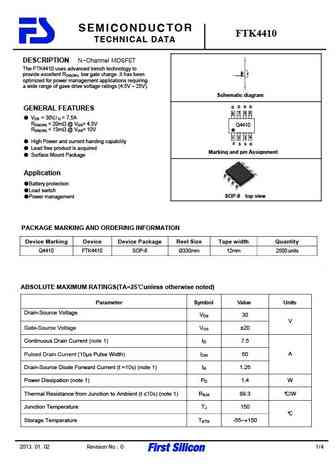
SEMICONDUCTOR FTK4410 TECHNICAL DATA DESCRIPTION N-Channel MOSFET The FTK4410 uses advanced trench technology to provide excellent RDS(ON), low gate charge .It has been optimized for power management applications requiring a wide range of gave drive voltage ratings (4.5V 25V). Schematic diagram D D D D GENERAL FEATURES 7 6 5 8 VDS = 30V,I = 7.5A D RDS(ON)
ao3410.pdf
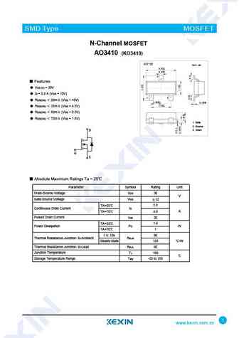
SMD Type MOSFET N-Channel MOSFET AO3410 (KO3410) SOT-23 Unit mm +0.1 2.9 -0.1 +0.1 0.4 -0.1 3 Features VDS (V) = 30V ID = 5.8 A (VGS = 10V) 1 2 RDS(ON) 28m (VGS = 10V) +0.1 +0.05 0.95-0.1 0.1 -0.01 +0.1 1.9 -0.1 RDS(ON) 33m (VGS = 4.5V) RDS(ON) 52m (VGS = 2.5V) RDS(ON) 70m (VGS = 1.8V) 1. Gate 2. Source 3. Drain
si9410dy.pdf
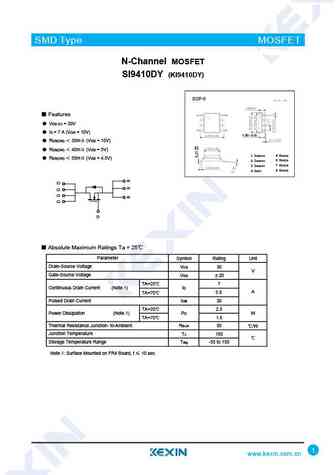
SMD Type MOSFET N-Channel MOSFET SI9410DY (KI9410DY) SOP-8 Features VDS (V) = 30V ID = 7 A (VGS = 10V) 1.50 0.15 RDS(ON) 30m (VGS = 10V) RDS(ON) 40m (VGS = 5V) 1 Source 5 Drain RDS(ON) 50m (VGS = 4.5V) 6 Drain 2 Source 7 Drain 3 Source 8 Drain 4 Gate Absolute Maximum Ratings Ta = 25 Parameter Symbol Rating Unit Drain-Sou
ao4410.pdf
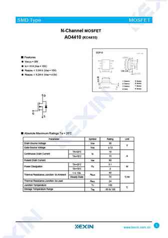
SMD Type MOSFET N-Channel MOSFET AO4410 (KO4410) SOP-8 Features VDS (V) = 30V ID = 18 A (VGS = 10V) RDS(ON) 5.5m (VGS = 10V) 1.50 0.15 RDS(ON) 6.2m (VGS = 4.5V) 1 Source 5 Drain 6 Drain 2 Source 7 Drain 3 Source 8 Drain 4 Gate D G S Absolute Maximum Ratings Ta = 25 Parameter Symbol Rating Unit Drain-Source Voltage VDS 30 V Gat
krf7410.pdf
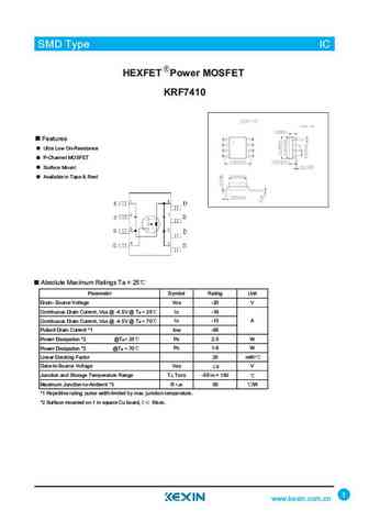
SMD Type IC SMD Type IC HEXFET Power MOSFET KRF7410 Features Ultra Low On-Resistance P-Channel MOSFET Surface Mount Available in Tape & Reel Absolute Maximum Ratings Ta = 25 Parameter Symbol Rating Unit Drain- Source Voltage VDS -20 V Continuous Drain Current, VGS @ -4.5V @ Ta =25 ID -16 Continuous Drain Current, VGS @ -4.5V @ Ta =70 ID -13 A Pulsed Drain Current *1 IDM -65 Power
si4410dy.pdf
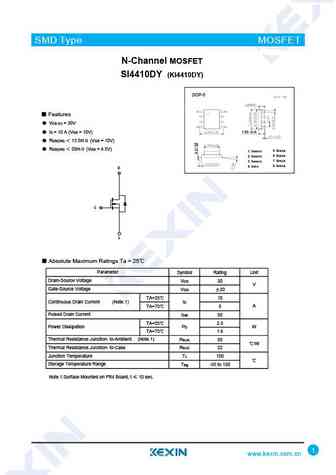
SMD Type MOSFET N-Channel MOSFET SI4410DY (KI4410DY) SOP-8 Features VDS (V) = 30V ID = 10 A (VGS = 10V) 1.50 0.15 RDS(ON) 13.5m (VGS = 10V) RDS(ON) 20m (VGS = 4.5V) 1 Source 5 Drain 6 Drain 2 Source 7 Drain 3 Source 8 Drain 4 Gate D G S Absolute Maximum Ratings Ta = 25 Parameter Symbol Rating Unit Drain-Source Voltage VDS 30 V
2sc4104.pdf
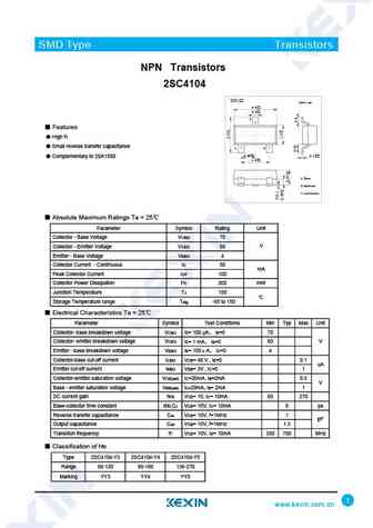
SMD Type Transistors NPN Transistors 2SC4104 SOT-23 Unit mm +0.1 2.9 -0.1 +0.1 0.4-0.1 3 Features High fT Small reverse transfer capacitance 1 2 +0.1 +0.05 0.95 -0.1 0.1 -0.01 Complementary to 2SA1580 +0.1 1.9 -0.1 1.Base 2.Emitter 3.collector Absolute Maximum Ratings Ta = 25 Parameter Symbol Rating Unit Collector - Base Voltage VCBO 70 Co
ao3410-3.pdf
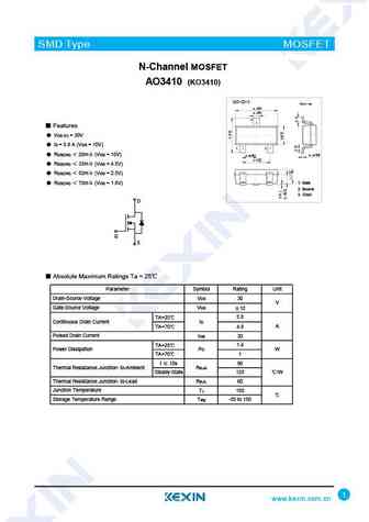
SMD Type MOSFET N-Channel MOSFET AO3410 (KO3410) SOT-23-3 Unit mm +0.2 2.9 -0.1 +0.1 0.4-0.1 3 Features VDS (V) = 30V ID = 5.8 A (VGS = 10V) 1 2 +0.02 +0.1 RDS(ON) 28m (VGS = 10V) 0.15 -0.02 0.95 -0.1 +0.1 1.9 -0.2 RDS(ON) 33m (VGS = 4.5V) RDS(ON) 52m (VGS = 2.5V) 1. Gate RDS(ON) 70m (VGS = 1.8V) 2. Source 3. Dr
ntr4101p.pdf
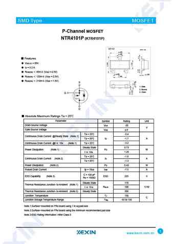
SMD Type MOSFET P-Channel MOSFET NTR4101P (KTR4101P) SOT-23 Unit mm +0.1 2.9 -0.1 +0.1 0.4 -0.1 3 Features VDS (V) =-20V ID =-3.2 A 1 2 RDS(ON) 85m (VGS =-4.5V) +0.1 +0.05 0.95-0.1 0.1-0.01 +0.1 1.9-0.1 RDS(ON) 120m (VGS =-2.5V) RDS(ON) 210m (VGS =-1.8V) S 1. Gate 2. Source 3. Drain G D Absolute Maximum Ratings Ta =
2sc4102.pdf
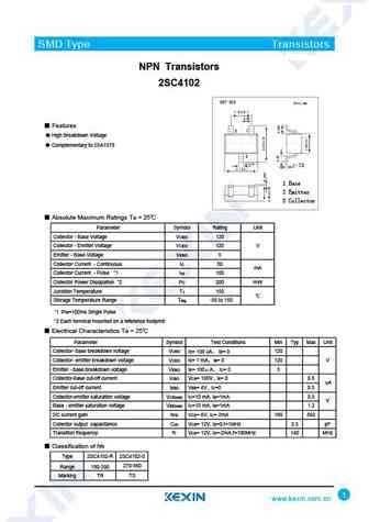
SMD Type Transistors NPN Transistors 2SC4102 Features High Breakdown Voltage Complementary to 2SA1579 1 Base 2 Emitter 3 Collector Absolute Maximum Ratings Ta = 25 Parameter Symbol Rating Unit Collector - Base Voltage VCBO 120 Collector - Emitter Voltage VCEO 120 V Emitter - Base Voltage VEBO 5 Collector Current - Continuous IC 50 mA Collector Current -
ntr4101p-3.pdf

SMD Type MOSFET P-Channel MOSFET NTR4101P (KTR4101P) SOT-23-3 Unit mm +0.2 2.9 -0.1 +0.1 0.4 -0.1 3 Features VDS (V) =-20V ID =-3.2 A 1 2 RDS(ON) 85m (VGS =-4.5V) +0.02 +0.1 0.15 -0.02 0.95 -0.1 +0.1 RDS(ON) 120m (VGS =-2.5V) 1.9 -0.2 RDS(ON) 210m (VGS =-1.8V) S 1. Gate 2. Source 3. Drain G D Absolute Maximum Rating
wfy4101.pdf
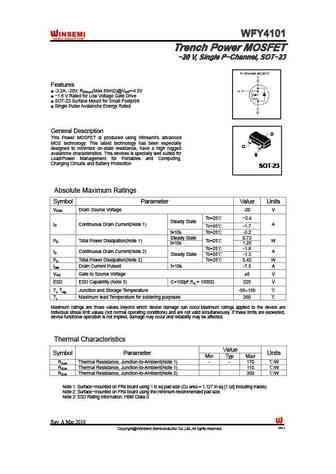
WFY4101 WFY4101 WFY4101 WFY4101 Trench Power MOSFET Trench Power MOSFET Trench Power MOSFET Trench Power MOSFET -20 V, Single P-Channel, SOT-23 -20 V, Single P-Channel, SOT-23 -20 V, Single P-Channel, SOT-23 -20 V, Single P-Channel, SOT-23 Features -3.2A, -20V, RDS(on)(Max 85m )@VGS=-4.5V -1.8 V Rated for Low Voltage Gate Drive SOT-23 Surface Mount for Small Footprin
chm9410jgp.pdf
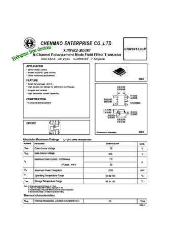
CHENMKO ENTERPRISE CO.,LTD CHM9410JGP SURFACE MOUNT N-Channel Enhancement Mode Field Effect Transistor VOLTAGE 30 Volts CURRENT 7 Ampere APPLICATION * Servo motor control. * Power MOSFET gate drivers. * Other switching applications. SO-8 FEATURE * Small flat package. (SO-8 ) ( ) * High density cell design for extremely low RDS(ON). 4.06 0.160 ( ) 3.70 0.146 * Rugged and relia
chm4410bjgp.pdf
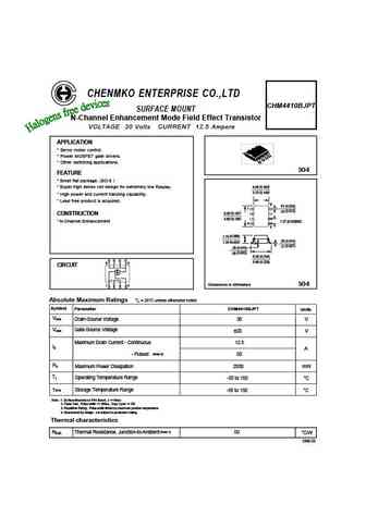
CHENMKO ENTERPRISE CO.,LTD CHM4410BJPT SURFACE MOUNT N-Channel Enhancement Mode Field Effect Transistor VOLTAGE 30 Volts CURRENT 12.5 Ampere APPLICATION * Servo motor control. * Power MOSFET gate drivers. * Other switching applications. SO-8 FEATURE * Small flat package. (SO-8 ) ( ) * Super high dense cell design for extremely low RDS(ON). 4.06 0.160 ( ) 3.70 0.146 * High pow
chm4410ajgp.pdf
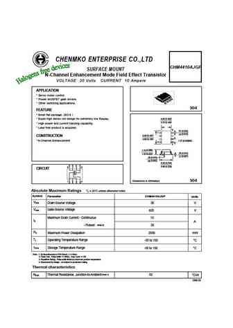
CHENMKO ENTERPRISE CO.,LTD CHM4410AJGP SURFACE MOUNT N-Channel Enhancement Mode Field Effect Transistor VOLTAGE 30 Volts CURRENT 10 Ampere APPLICATION * Servo motor control. * Power MOSFET gate drivers. * Other switching applications. SO-8 FEATURE * Small flat package. (SO-8 ) ( ) * Super high dense cell design for extremely low RDS(ON). 4.06 0.160 ( ) 3.70 0.146 * High power
chm0410jgp.pdf
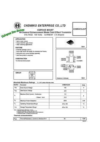
CHENMKO ENTERPRISE CO.,LTD CHM0410JGP SURFACE MOUNT N-Channel Enhancement Mode Field Effect Transistor VOLTAGE 100 Volts CURRENT 3.4 Ampere APPLICATION * Servo motor control. * Power MOSFET gate drivers. * Other switching applications. SO-8 FEATURE * Small flat package. (SO-8 ) ( ) * Super high dense cell design for extremely low RDS(ON). 4.06 0.160 ( ) 3.70 0.146 * High power
chm8410jgp.pdf
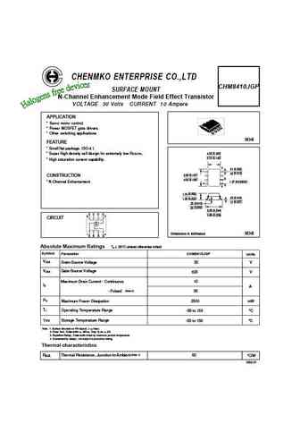
CHENMKO ENTERPRISE CO.,LTD CHM8410JGP SURFACE MOUNT N-Channel Enhancement Mode Field Effect Transistor VOLTAGE 30 Volts CURRENT 10 Ampere APPLICATION * Servo motor control. * Power MOSFET gate drivers. * Other switching applications. SO-8 FEATURE * Small flat package. (SO-8 ) ( ) * Super High density cell design for extremely low RDS(ON). 4.06 0.160 ( ) 3.70 0.146 * High satu
csd16410q5a.pdf
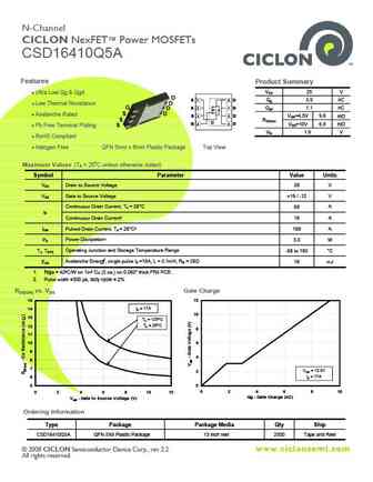
N-Channel CICLON NexFET Power MOSFETs CSD16410Q5A Features Product Summary Ultra Low Qg & Qgd VDS 25 V D S 1 8 D S 1 8 D Qg 3.9 nC Low Thermal Resistance D S 2 7 D G S 2 7 D Qgd 1.1 nC D Avalanche Rated S D S 3 6 D S 3 6 D VGS=4.5V 9.6 m S RDS(on) D D G 4 5 D G 4 5 D VGS=10V 6.8 m Pb Free Terminal Plating S Vth 1.9 V RoHS Complian
mrf410.pdf
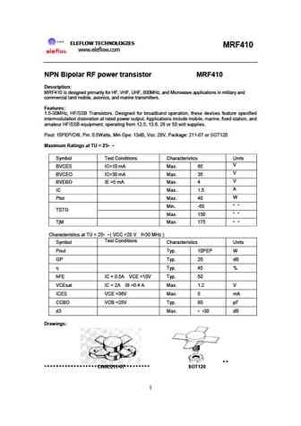
ELEFLOW TECHNOLOGIES MRF410 www.eleflow.com NPN Bipolar RF power transistor MRF410 Description MRF410 is designed primarily for HF, VHF, UHF, 800MHz, and Microwave applications in military and commercial land mobile, avionics, and marine transmitters. Features 1.5-30MHz, HF/SSB Transistors. Designed for broadband operation, these devices feature specified intermodulation dist
elm33410ca.pdf
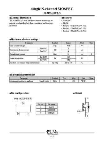
Single N-channel MOSFET ELM33410CA-S General description Features ELM33410CA-S uses advanced trench technology to Vds=20V provide excellent Rds(on), low gate charge and low gate Id=5A resistance. Rds(on)
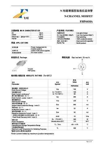
gsm3410.pdf
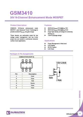
GSM3410 30V N-Channel Enhancement Mode MOSFET Product Description Features GSM3410, N-Channel enhancement mode 30V/6.0A,RDS(ON)=27m @VGS=10V MOSFET, uses Advanced Trench Technology to 30V/4.5A,RDS(ON)=30m @VGS=4.5V provide excellent RDS (ON), low gate charge. Super high density cell design for extremely low RDS (ON) These devices are particularly suited for low TSOP-6 p
gsm4102w.pdf
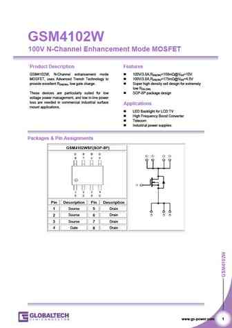
GSM4102W 100V N-Channel Enhancement Mode MOSFET Product Description Features GSM4102W, N-Channel enhancement mode 100V/3.8A,RDS(ON)=158m @VGS=10V MOSFET, uses Advanced Trench Technology to 100V/3.0A,RDS(ON)=175m @VGS=4.5V provide excellent RDS(ON), low gate charge. Super high density cell design for extremely low RDS (ON) These devices are particularly suited for
hy3410p hy3410m hy3410b hy3410ps hy3410pm hy3410mf.pdf
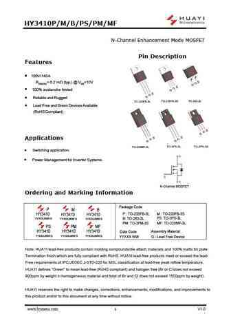
HY3410P/M/B/PS/PM/MF N-Channel Enhancement Mode MOSFET Pin Description F eatures 100V/140A S RDS(ON)= 6.2 m (typ.) @ VGS=10V D G S D 100% avalanche tested G S D G Reliable and Rugged TO-220FB-3L TO-220FB-3S TO-263-2L Lead Free and Green Devices Available (RoHS Compliant) S D G S S pplications D A D G G TO-3PS-3L TO-3PM-3S TO-220MF-3L Sw
mmn4410.pdf
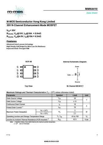
MMN4410 Data Sheet M-MOS Semiconductor Hong Kong Limited 30V N-Channel Enhancement-Mode MOSFET VDS= 30V RDS(ON), Vgs@10V, Ids@18A = 5.5m RDS(ON), Vgs@4.5V, Ids@15A = 6.2m Features Advanced trench process technology High Density Cell Design For Ultra Low On-Resistance Improved Shoot-Through FOM SOP-08 Internal Schematic Diagram Drain Gate Source Top View N-Channel MOSFET
pa410bd.pdf
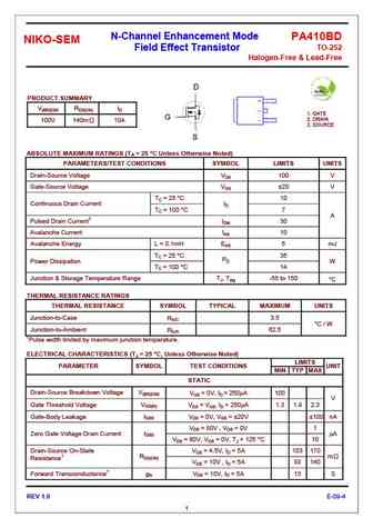
N-Channel Enhancement Mode PA410BD NIKO-SEM TO-252 Field Effect Transistor Halogen-Free & Lead-Free D PRODUCT SUMMARY V(BR)DSS RDS(ON) ID 1. GATE G 2. DRAIN 100V 140m 10A 3. SOURCE S ABSOLUTE MAXIMUM RATINGS (TA = 25 C Unless Otherwise Noted) PARAMETERS/TEST CONDITIONS SYMBOL LIMITS UNITS Drain-Source Voltage VDS 100 V Gate-Source Voltage VGS 20 V TC =
pp1410aea.pdf
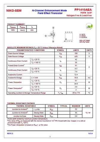
PP1410AEA N-Channel Enhancement Mode NIKO-SEM PDFN 3x3P Field Effect Transistor Halogen-Free & Lead-Free PRODUCT SUMMARY V(BR)DSS RDS(ON) ID D 100V 14m 42A D D D D G. GATE D. DRAIN G S. SOURCE 100% UIS Tested #1 S S S G S 100% Rg Tested ABSOLUTE MAXIMUM RATINGS (TA = 25 C Unless Otherwise Noted) PARAMETERS/TEST CONDITIONS SYMBOL LIMITS UNITS Drain-Sou
p1410bd.pdf
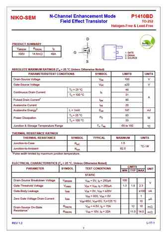
N-Channel Enhancement Mode P1410BD NIKO-SEM TO-252 Field Effect Transistor Halogen-Free & Lead-Free D PRODUCT SUMMARY V(BR)DSS RDS(ON) ID 1. GATE G 100V 14.5m 49A 2. DRAIN 3. SOURCE S ABSOLUTE MAXIMUM RATINGS (TA = 25 C Unless Otherwise Noted) PARAMETERS/TEST CONDITIONS SYMBOL LIMITS UNITS Drain-Source Voltage VDS 100 V Gate-Source Voltage VGS 20 V TC =
p1410bk.pdf
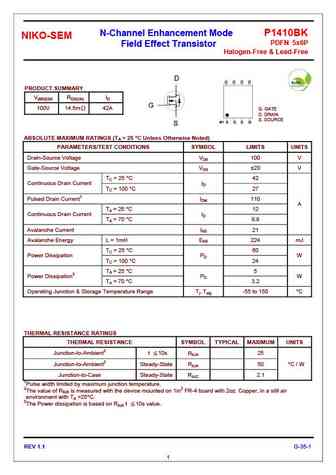
N-Channel Enhancement Mode P1410BK NIKO-SEM PDFN 5x6P Field Effect Transistor Halogen-Free & Lead-Free D D D D D PRODUCT SUMMARY V(BR)DSS RDS(ON) ID G 100V 14.5m 42A G. GATE D. DRAIN S. SOURCE #1 S S S G S ABSOLUTE MAXIMUM RATINGS (TA = 25 C Unless Otherwise Noted) PARAMETERS/TEST CONDITIONS SYMBOL LIMITS UNITS Drain-Source Voltage VDS 100 V Gate-Source Vo
pa410btf.pdf
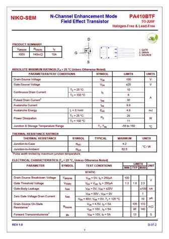
N-Channel Enhancement Mode PA410BTF NIKO-SEM TO-220F Field Effect Transistor Halogen-Free & Lead-Free D PRODUCT SUMMARY V(BR)DSS RDS(ON) ID 1. GATE 2. DRAIN G 100V 140m 10A 3. SOURCE S ABSOLUTE MAXIMUM RATINGS (TA = 25 C Unless Otherwise Noted) PARAMETERS/TEST CONDITIONS SYMBOL LIMITS UNITS Drain-Source Voltage VDS 100 V Gate-Source Voltage VGS 20 V TC
pp1410ak.pdf
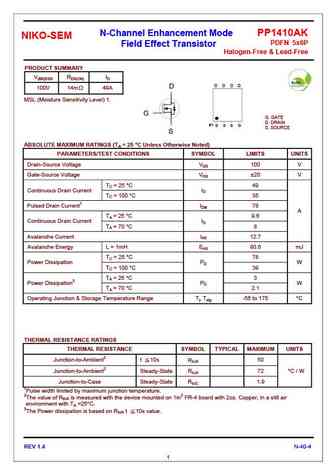
N-Channel Enhancement Mode PP1410AK NIKO-SEM PDFN 5x6P Field Effect Transistor Halogen-Free & Lead-Free PRODUCT SUMMARY V(BR)DSS RDS(ON) ID D D D D D 100V 14m 49A MSL (Moisture Sensitivity Level) 1. G G. GATE D. DRAIN #1 S S S G S. SOURCE S ABSOLUTE MAXIMUM RATINGS (TA = 25 C Unless Otherwise Noted) PARAMETERS/TEST CONDITIONS SYMBOL LIMITS UNITS Drain-Sou
pp1410af.pdf
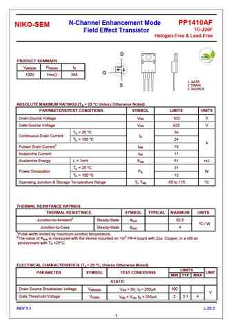
N-Channel Enhancement Mode PP1410AF NIKO-SEM TO-220F Field Effect Transistor Halogen-Free & Lead-Free D PRODUCT SUMMARY V(BR)DSS RDS(ON) ID G 100V 14m 34A 1. GATE 2. DRAIN S 3. SOURCE ABSOLUTE MAXIMUM RATINGS (TA = 25 C Unless Otherwise Noted) PARAMETERS/TEST CONDITIONS SYMBOL LIMITS UNITS Drain-Source Voltage VDS 100 V Gate-Source Voltage VGS 20 V TC =
pp1410ad.pdf
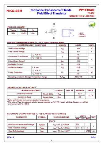
N-Channel Enhancement Mode PP1410AD NIKO-SEM TO-252 Field Effect Transistor Halogen-Free & Lead-Free D PRODUCT SUMMARY V(BR)DSS RDS(ON) ID G 1.GATE 100V 14m 45A 2.DRAIN 3.SOURCE S ABSOLUTE MAXIMUM RATINGS (TA = 25 C Unless Otherwise Noted) PARAMETERS/TEST CONDITIONS SYMBOL LIMITS UNITS Drain-Source Voltage VDS 100 V Gate-Source Voltage VGS 20 V TC = 25
pmc4106.pdf
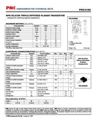
PMC4106 NPN SILICON TRIPLE DIFFUSED PLANAR TRANSISTOR designed for switching regulator applications. TO-220AB MAXIMUM RATINGS (Ta = 25 C) Characteristic Symbol Value Unit Collector to base voltage VCBO 500 V Collector to emitter voltage VCEO 400 V Emitter to base voltage VEBO 7 V Collector current IC 7 A Collector current (peak) IC(peak) 14 A Base Current IB 3 A Collector
shd226410.pdf
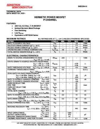
SENSITRON SHD226410 SEMICONDUCTOR TECHNICAL DATA DATA SHEET 621, REV - HERMETIC POWER MOSFET P-CHANNEL FEATURES -200 Volt, 0.5 Ohm, -7.7A MOSFET Isolated Hermetic Metal Package Fast Switching Low RDS (on) Equivalent to IRFY9240 Series MAXIMUM RATINGS ALL RATINGS ARE AT TC = 25 C UNLESS OTHERWISE SPECIFIED. RATING SYMBOL MIN. TYP. MAX. UNITS GATE TO SOURCE VOLTA
shd219410.pdf
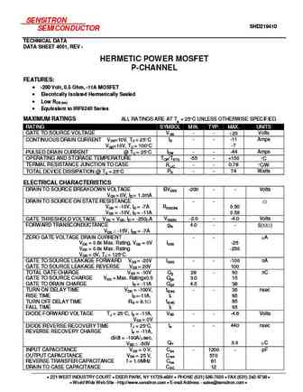
SENSITRON SHD219410 SEMICONDUCTOR TECHNICAL DATA DATA SHEET 4001, REV - HERMETIC POWER MOSFET P-CHANNEL FEATURES -200 Volt, 0.5 Ohm, -11A MOSFET Electrically Isolated Hermetically Sealed Low RDS (on) Equivalent to IRF9240 Series MAXIMUM RATINGS ALL RATINGS ARE AT TA = 25 C UNLESS OTHERWISE SPECIFIED. RATING SYMBOL MIN. TYP. MAX. UNITS GATE TO SOURCE VOLTAGE VGS -
ssm9410gm.pdf
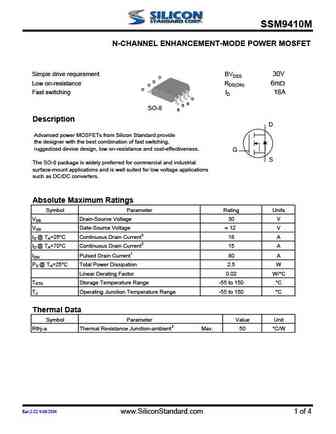
SSM9410M N-CHANNEL ENHANCEMENT-MODE POWER MOSFET Simple drive requirement BVDSS 30V D D Low on-resistance RDS(ON) 6m D D Fast switching ID 18A G S S SO-8 S Description D Advanced power MOSFETs from Silicon Standard provide the designer with the best combination of fast switching, ruggedized device design, low on-resistance and cost-effectiveness. G S The SO-8 package is
ssm4410m.pdf
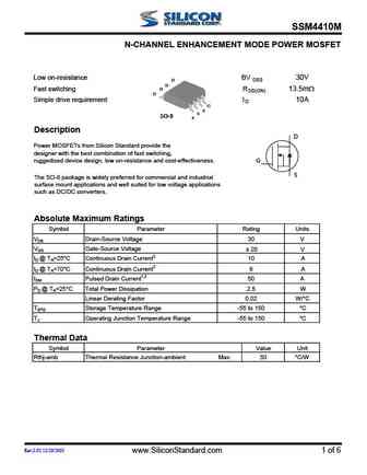
SSM4410M N-CHANNEL ENHANCEMENT MODE POWER MOSFET Low on-resistance BV 30V DSS D D Fast switching D RDS(ON) 13.5m D Simple drive requirement I 10A D G S S SO-8 S Description D Power MOSFETs from Silicon Standard provide the designer with the best combination of fast switching, ruggedized device design, low on-resistance and cost-effectiveness. G S The SO-8 package is wid
sl4410.pdf
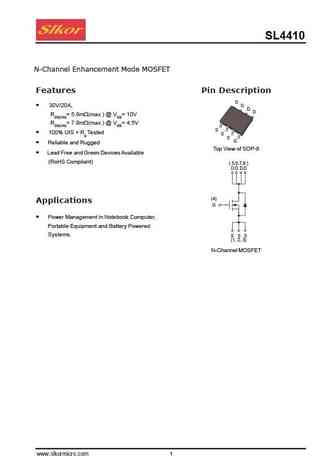
SL4410 N-Channel Enhancement Mode MOSFET Features Pin Description D D 30V/20A, D D RDS(ON)= 5.9m (max.) @ VGS= 10V RDS(ON)= 7.9m (max.) @ VGS= 4.5V S 100% UIS + Rg Tested S S G Reliable and Rugged Top View of SOP-8 Lead Free and Green Devices Available (RoHS Compliant) ( 5,6,7,8 ) D D D D (4) Applications G Power Management in Notebook Computer, Portable Equipm
stn4102.pdf
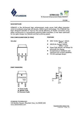
STN4102 N Channel Enhancement Mode MOSFET 15.0A DESCRIPTION STN4102 is the N-Channel logic enhancement mode power field effect transistor which is produced using high cell density, DMOS trench technology. The STN410D has been designed specially to improve the overall efficiency of DC/DC converters using either synchronous or conventional switching PWM controllers. It has been op
stn410d.pdf
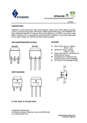
STN410D N Channel Enhancement Mode MOSFET 15.0A DESCRIPTION STN410D is the N-Channel logic enhancement mode power field effect transistor which is produced using high cell density, DMOS trench technology. The STN410D has been designed specially to improve the overall efficiency of DC/DC converters using either synchronous or conventional switching PWM controllers. It has been o
qm2410j.pdf
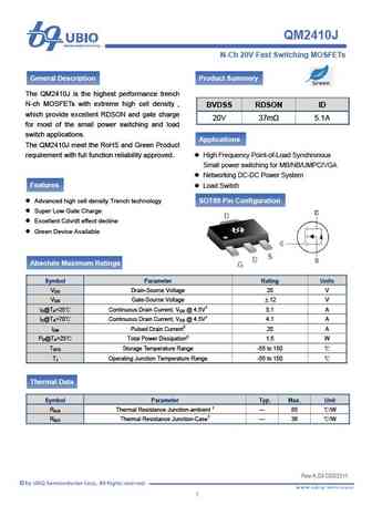
QM2410J N-Ch 20V Fast Switching MOSFETs General Description Product Summery The QM2410J is the highest performance trench N-ch MOSFETs with extreme high cell density , BVDSS RDSON ID which provide excellent RDSON and gate charge 20V 37m 5.1A for most of the small power switching and load switch applications. Applications The QM2410J meet the RoHS and Green Product requi
qm2410k.pdf
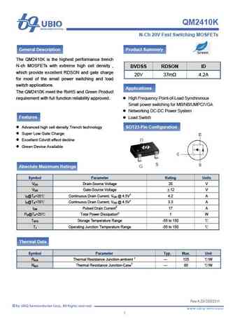
QM2410K N-Ch 20V Fast Switching MOSFETs General Description Product Summery The QM2410K is the highest performance trench N-ch MOSFETs with extreme high cell density , BVDSS RDSON ID which provide excellent RDSON and gate charge 20V 37m 4.2A for most of the small power switching and load switch applications. Applications The QM2410K meet the RoHS and Green Product requir
qm2410d.pdf
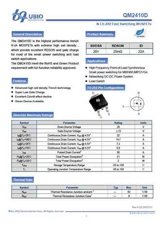
QM2410D N-Ch 20V Fast Switching MOSFETs General Description Product Summery The QM2410D is the highest performance trench N-ch MOSFETs with extreme high cell density , BVDSS RDSON ID which provide excellent RDSON and gate charge 20V 25m 22A for most of the small power switching and load switch applications. Applications The QM2410D meet the RoHS and Green Product require
qm2410s.pdf
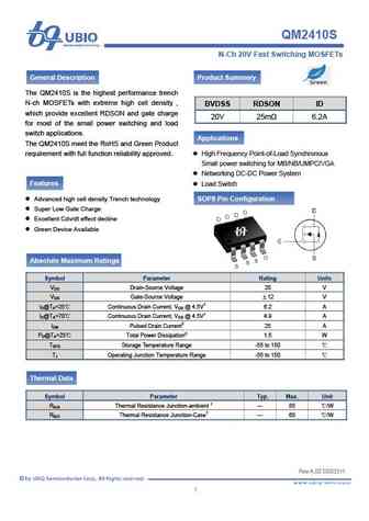
QM2410S N-Ch 20V Fast Switching MOSFETs General Description Product Summery The QM2410S is the highest performance trench N-ch MOSFETs with extreme high cell density , BVDSS RDSON ID which provide excellent RDSON and gate charge 20V 25m 6.2A for most of the small power switching and load switch applications. Applications The QM2410S meet the RoHS and Green Product requi
qm2410g.pdf
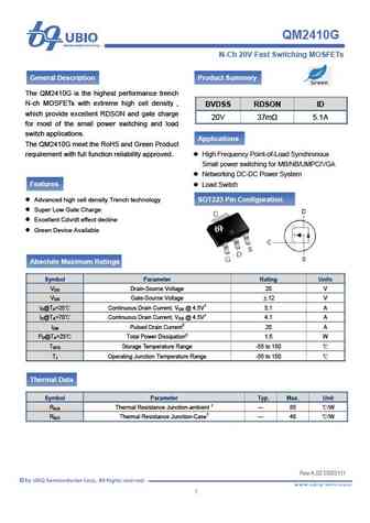
QM2410G N-Ch 20V Fast Switching MOSFETs General Description Product Summery The QM2410G is the highest performance trench N-ch MOSFETs with extreme high cell density , BVDSS RDSON ID which provide excellent RDSON and gate charge 20V 37m 5.1A for most of the small power switching and load switch applications. Applications The QM2410G meet the RoHS and Green Product requi
qn4103m6n.pdf
uPI SEMI www.upi-semi.com Power Solutions for TODAY and TOMORROW IS NOW PART OF Please visit our website for more information www.upi-semi.com The contents of this document are provided in connection with uPI Semiconductor Corp. ( uPI ) products. uPI makes no representations or warranties with respect to the accuracy or completeness of the contents of this publication and res
qm2410v.pdf
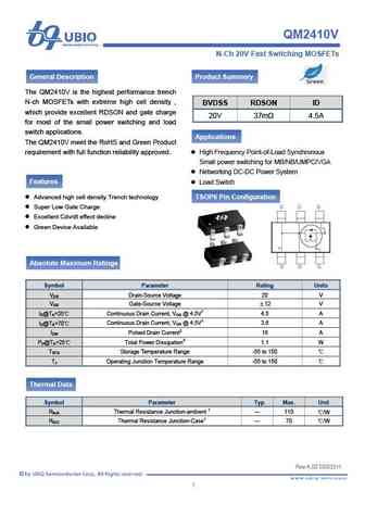
QM2410V N-Ch 20V Fast Switching MOSFETs General Description Product Summery The QM2410V is the highest performance trench N-ch MOSFETs with extreme high cell density , BVDSS RDSON ID which provide excellent RDSON and gate charge 20V 37m 4.5A for most of the small power switching and load switch applications. Applications The QM2410V meet the RoHS and Green Product requir
cs3410b3.pdf

Silicon N-Channel Power MOSFET R CS3410 B3 General Description VDSS 100 V CS3410 B3, the silicon N-channel Enhanced VDMOSFETs, is ID 17 A PD (TC=25 ) 80 W obtained by the self-aligned planar Technology which reduce the RDS(ON)Typ 0.075 conduction loss, improve switching performance and enhance the avalanche energy. The transistor can be used in various power
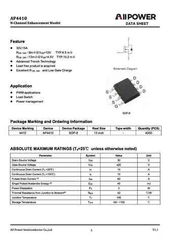
asdm4410s.pdf
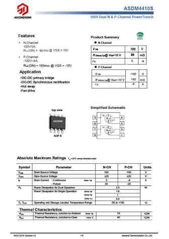
ASDM4410S 100V Dual N & P-Channel PowerTrench Features Product Summary N-Channel V DS 100 V V DS V 100 95 95 R DS(on),Typ@ VGS=10 V m R DS(on),Typ@ VGS=10 V m 5 I A I D RDS (ON) = 185m @ VGS = -10V P-Channel Application V DS -100 V DC-DC primary bridge 185 R DS(on),Typ@ VGS=-10 V m DC-DC Synchronous rectification I D -4 A Hot
et4410.pdf
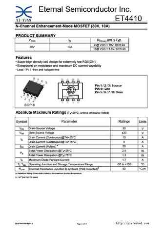
Eternal Semiconductor Inc. ET4410 N-Channel Enhancement-Mode MOSFET (30V, 10A) PRODUCT SUMMARY VDSS ID RDS(on) (m ) Typ. 9 @ VGS = 10V, ID=6.9A 30V 10A 13@ VGS = 4.5V, ID=5.8A Features Super high density cell design for extremely low RDS(ON) Exceptional on-resistance and maximum DC current capability Lead Pb -free and halogen-free Pin 1 / 2 / 3 Source Pin 4 Gate
hsm4410.pdf
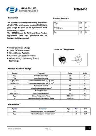
HSM4410 Description Product Summary The HSM4410 is the high cell density trenched N- VDS 30 V ch MOSFETs, which provide excellent RDSON and gate charge for most of the synchronous buck RDS(ON),max 9.5 m converter applications. ID 12 A The HSM4410 meet the RoHS and Green Product requirement, 100% EAS guaranteed with full function reliability approved. l Super Low Gate C
hsm4103.pdf
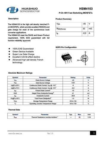
HSM4103 P-Ch 40V Fast Switching MOSFETs Description Product Summary VDS -40 V The HSM4103 is the high cell density trenched P- ch MOSFETs, which provide excellent RDSON and RDS(ON),max 32 m gate charge for most of the synchronous buck converter applications. ID -8.6 A The HSM4103 meet the RoHS and Green Product requirement, 100% EAS guaranteed with full function reli
hsu4103.pdf
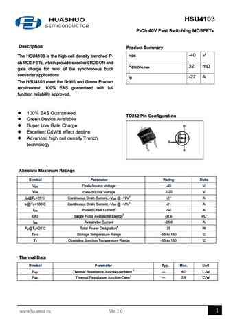
HSU4103 P-Ch 40V Fast Switching MOSFETs Description Product Summary VDS -40 V The HSU4103 is the high cell density trenched P- ch MOSFETs, which provide excellent RDSON and RDS(ON),max 32 m gate charge for most of the synchronous buck converter applications. ID -27 A The HSU4103 meet the RoHS and Green Product requirement, 100% EAS guaranteed with full function reliab
2n4265 2n4400 2n4401 2n4402 2n4403 2n4409 2n4410 2n4424 2n4425 2n4951 2n4952 2n4953 2n4954 2n5087 2n5088 2n5089.pdf
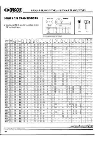
jmcl0410aud.pdf
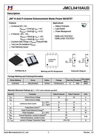
JMCL0410AUD Description JMT N And P-channel Enhancement Mode Power MOSFET Features Applications N-channel 40V, 14A Battery Protection RDS(ON)
jmcl0410agd.pdf
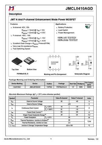
JMCL0410AGD Description JMT N And P-channel Enhancement Mode Power MOSFET Features Applications N-channel 40V, 16A Battery Protection RDS(ON)
irfr3410.pdf
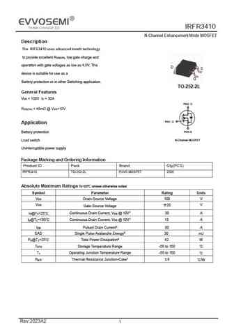
IRFR3410 N-Channel Enhancement Mode MOSFET Description The IRFR3410 uses advanced trench technology to provide excellent R , low gate charge and DS(ON) operation with gate voltages as low as 4.5V. This D S device is suitable for use as a G Battery protection or in other Switching application. TO-252-2L General Features V = 100V I = 30A DS D PIN2 D R
irfl4105.pdf
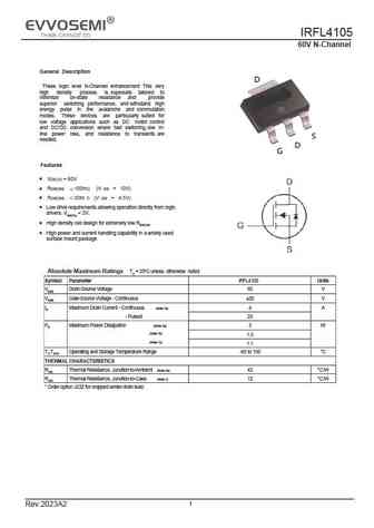
IRFL4105 60V N-Channel General Description These logic level N-Channel enhancement This very high density process is especially tailored to minimize on-state resistance and provide superior switching performance, and withstand high energy pulse in the avalanche and commutation modes. These devices are particularly suited for low voltage applications such as DC motor control a
htd410p06.pdf
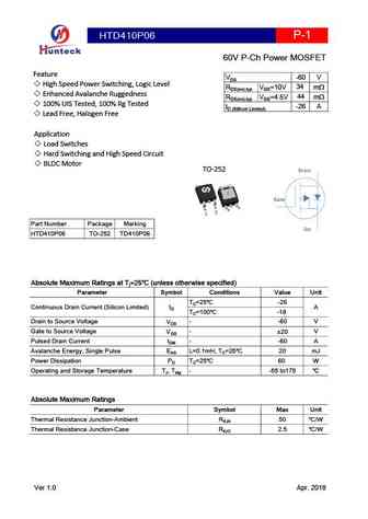
HTD410P06 P-1 60V P-Ch Power MOSFET Feature -60 V VDS High Speed Power Switching, Logic Level 34 RDS(on),typ VGS=10V m Enhanced Avalanche Ruggedness 44 RDS(on),typ VGS=4.5V m 100% UIS Tested, 100% Rg Tested -26 A ID (Sillicon Limited) Lead Free, Halogen Free Application Load Switches Hard Switching and High Speed Circuit BLDC Motor TO-252 Dr
hts410p06.pdf
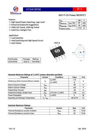
HTS410P06 P-1 60V P-Ch Power MOSFET Feature -60 V VDS High Speed Power Switching, Logic Level 35 RDS(on),typ VGS=10V m Enhanced Avalanche Ruggedness 45 RDS(on),typ VGS=4.5V m 100% UIS Tested, 100% Rg Tested -7.5 A ID (Sillicon Limited) Lead Free, Halogen Free Application Load Switches Hard Switching and High Speed Circuit SOIC-8 BLDC Motor 2
4410.pdf
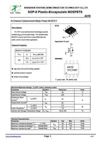
SHENZHEN TUOFENG SEMICONDUCTOR TECHNOLOGY CO.,LTD SOP-8 Plastic-Encapsulate MOSFETS 4410 N-Channel Enhancement Mode Power MOSFET SO-8L D D Description D D The 4410 uses advanced trench technology to provide G G S excellent RDS(ON) and low gate charge . The complementary S S S S MOSFETs may be used to form a level shifted high side SO-8 S Pin 1 switch, and for a host o
7410.pdf
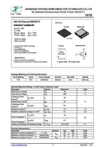
SHENZHEN TUOFENG SEMICONDUCTOR TECHNOLOGY CO.,LTD N-Channel Enhancement Mode Power MOSFET 7410 30V N-Channel MOSFET DFN 3x3_EP PRODUCT SUMMARY Top View Bottom View VDS (V) = 30V ID =24A RDS(ON)
tf3410.pdf
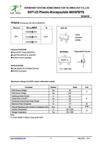
SHENZHEN TUOFENG SEMICONDUCTOR TECHNOLOGY CO.,LTD SOT-23 Plastic-Encapsulate MOSFETS 3410 TF TF N-Channel 30-V(D-S) MOSFET 3410 V(BR)DSS RDS(on)MAX ID SOT-23 0.028 @ 10V 3 1.GATE 30V 5.8A 0.033 @ 4.5V 2.SOURCE 3.DRAIN 1 0.042 @ 2.5V 2 General FEATURE Equivalent Circuit MARKING TrenchFET Power MOSFET Lead free product is acquired Surface mount package AA1TF w
wsp4410.pdf
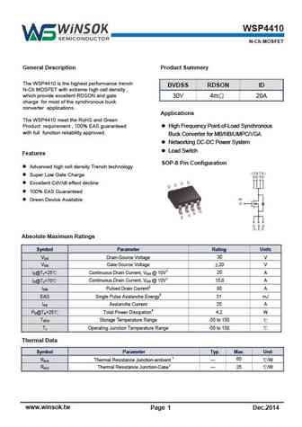
WSP4410 N-Ch MOSFET General Description Product Summery The WSP4410 is the highest performance trench BVDSS RDSON ID N-Ch MOSFET with extreme high cell density , which provide excellent RDSON and gate 30V 4m 20A charge for most of the synchronous buck converter applications . Applications The WSP4410 meet the RoHS and Green High Frequency Point-of-Load Synchronous Prod
wsf3410.pdf
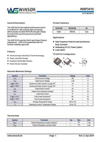
WSF3410 N-Ch MOSFET Product Summery General Description The WSF3410 is the highest performance trench BVDSS RDSON ID N-ch MOSFET with extreme high cell density , which provide excellent RDSON and gate charge 100V 90m 15A for most of the synchronous buck converter applications . Applications The WSF3410 meet the RoHS and Green Product High Frequency Point-of-Load Synchrono
vs4410at.pdf
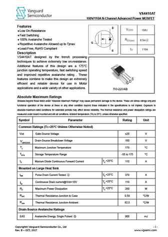
VS4410AT 100V/110A N-Channel Advanced Power MOSFET Features Low On-Resistance Fast Switching 100% Avalanche Tested Repetitive Avalanche Allowed up to Tjmax Lead-Free, RoHS Compliant Description VS4410AT designed by the trench processing techniques to achieve extremely low on-resistance. Additional features of this design are a 175 C junction opera
sm4410.pdf
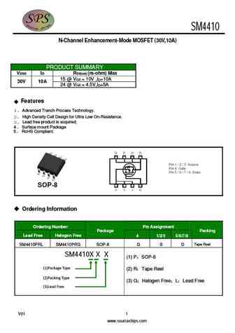
SM4410 N-Channel Enhancement-Mode MOSFET (30V,10A) PRODUCT SUMMARY VDSS ID RDS(on) (m-ohm) Max 15 @ VGS = 10V ,ID=10A 30V 10A 24 @ VGS = 4.5V,ID=5A Features 1 Advanced Trench Process Technology. 2 High Density Cell Design for Ultra Low On-Resistance. 3 Lead free product is acquired . 4 Surface mount Package 5 RoHS Compliant. Ordering
si4410bdy.pdf

SI4410BDY www.VBsemi.tw N-Channel 20V (D-S) MOSFET FEATURES PRODUCT SUMMARY Halogen-free VDS (V) RDS(on) ( ) ID (A)a Qg (Typ.) TrenchFET Power MOSFET 0.012 at VGS = 10 V 12 20 6.1 nC Optimized for High-Side Synchronous 0.015 at VGS = 4.5 V 11 Rectifier Operation 100 % Rg Tested 100 % UIS Tested APPLICATIONS Notebook CPU Core - High-Side Switch S
nts4101pt1g.pdf
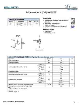
NTS4101PT1G www.VBsemi.tw P-Channel 20 V (D-S) MOSFET FEATURES PRODUCT SUMMARY Halogen-free According to IEC 61249-2-21 VDS (V) RDS(on) ( )ID (A)c Qg (Typ.) Definition 0.080 at VGS = - 4.5 V - 3.1 TrenchFET Power MOSFET 4.3 nC - 20 0.100 at VGS = - 2.5 V - 2.3 100 % Rg Tested Compliant to RoHS Directive 2002/95/EC APPLICATIONS Load Switch DC/DC Conv
si4410dy-t1.pdf
SI4410DY-T1 www.VBsemi.tw N-Channel 20V (D-S) MOSFET FEATURES PRODUCT SUMMARY Halogen-free VDS (V) RDS(on) ( ) ID (A)a Qg (Typ.) TrenchFET Power MOSFET 0.012 at VGS = 10 V 12 20 6.1 nC Optimized for High-Side Synchronous 0.015 at VGS = 4.5 V 11 Rectifier Operation 100 % Rg Tested 100 % UIS Tested APPLICATIONS Notebook CPU Core - High-Side Switch
irfu3410p.pdf
IRFU3410P www.VBsemi.tw www.VBsemi.tw N-Channel 100 V (D-S) MOSFET FEATURES PRODUCT SUMMARY TrenchFET Power MOSFET VDS (V) RDS(on) ( )ID (A) 175 C Junction Temperature 100 0.036 at VGS = 10 V 35 PWM Optimized 100 % Rg Tested Compliant to RoHS Directive 2002/95/EC TO-251 APPLICATIONS Primary Side Switch D G S G D S N-Channel MOSFET Top View
vbfb1410.pdf
VBFB1410 www.VBsemi.com N-Channel 40 V (D-S) MOSFET FEATURES PRODUCT SUMMARY Halogen-free According to IEC 61249-2-21 VDS (V) RDS(on) ( ) ID (A) Qg (Typ.) Definition 0.0 3 at VGS = 10 V 55d TrenchFET Power MOSFET 40 9.5 0.0 at VGS = 4.5 V 5d 100 % Rg and UIS Tested Compliant to RoHS Directive 2002/95/EC APPLICATIONS TO-251 Power Supply - Secondary
aod410.pdf
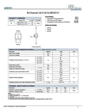
AOD410 www.VBsemi.tw N-Channel 30-V (D-S) MOSFET FEATURES PRODUCT SUMMARY TrenchFET Power MOSFET VDS (V) RDS(on) ( ) ID (A)a, e Qg (Typ) 100 % Rg and UIS Tested Compliant to RoHS Directive 2011/65/EU 0.007 at VGS = 10 V 50 30 25 nC 0.009 at VGS = 4.5 V 40 APPLICATIONS D OR-ing Server TO-252 DC/DC G G D S S Top View N-Channel MOSFET ABSOLUT
si9410bdy-t1.pdf
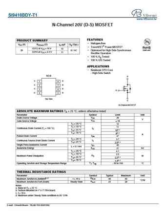
SI9410BDY-T1 www.VBsemi.tw N-Channel 20V (D-S) MOSFET FEATURES PRODUCT SUMMARY Halogen-free VDS (V) RDS(on) ( ) ID (A)a Qg (Typ.) TrenchFET Power MOSFET 0.012 at VGS = 10 V 12 20 6.1 nC Optimized for High-Side Synchronous 0.015 at VGS = 4.5 V 11 Rectifier Operation 100 % Rg Tested 100 % UIS Tested APPLICATIONS Notebook CPU Core - High-Side Switch
irlr3410tr.pdf
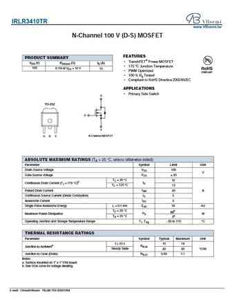
IRLR3410TR www.VBsemi.tw N-Channel 100 V (D-S) MOSFET FEATURES PRODUCT SUMMARY TrenchFET Power MOSFET VDS (V) RDS(on) ( )ID (A) 175 C Junction Temperature 100 0.11 4 at VGS = 10 V 15 PWM Optimized 100 % Rg Tested Compliant to RoHS Directive 2002/95/EC APPLICATIONS Primary Side Switch D TO-252 G S G D S N-Channel MOSFET ABSOLUTE MAXIMUM RATING
irf3410.pdf
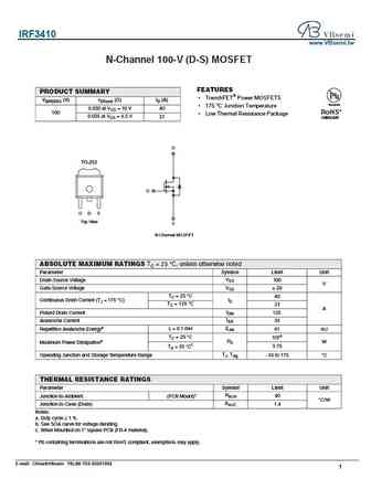
IRF3410 www.VBsemi.tw N-Channel 100-V (D-S) MOSFET FEATURES PRODUCT SUMMARY TrenchFET Power MOSFETS V(BR)DSS (V) rDS(on) ( )ID (A) Available 175 C Junction Temperature 0.030 at VGS = 10 V 40 RoHS* 100 Low Thermal Resistance Package 0.035 at VGS = 4.5 V 37 COMPLIANT D TO-252 G G D S Top View S N-Channel MOSFET ABSOLUTE MAXIMUM RATINGS TC = 25 C, unless
nds9410a.pdf
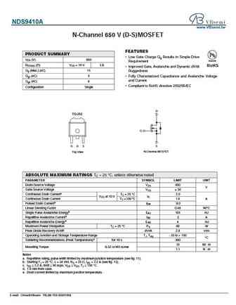
NDS9410A www.VBsemi.tw N-Channel 650 V (D-S) MOSFET FEATURES PRODUCT SUMMARY Low Gate Charge Qg Results in Simple Drive VDS (V) 650 Available Requirement RDS(on) ( )VGS = 10 V 3.8 RoHS Improved Gate, Avalanche and Dynamic dV/dt Qg (Max.) (nC) 15 Ruggedness Qgs (nC) 3 Fully Characterized Capacitance and Avalanche Voltage and Current Qgd (nC) 6 Compliant to RoHS
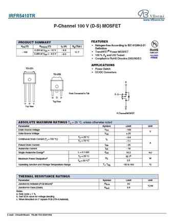
irfr4104trpbf.pdf
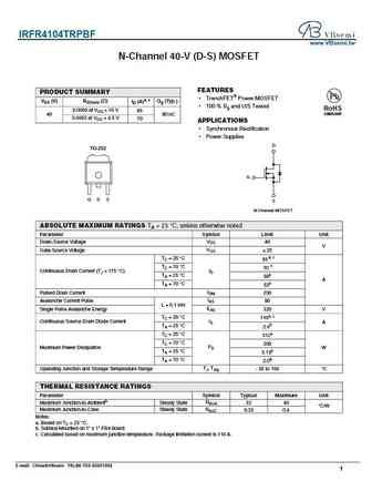
IRFR4104TRPBF www.VBsemi.tw N-Channel 40-V (D-S) MOSFET FEATURES PRODUCT SUMMARY TrenchFET Power MOSFET VDS (V) RDS(on) ( ) ID (A)a, c Qg (Typ.) 100 % Rg and UIS Tested RoHS 0.0050 at VGS = 10 V 85 COMPLIANT 40 80 nC 0.0065 at VGS = 4.5 V 70 APPLICATIONS Synchronous Rectification Power Supplies D TO-252 G G D S S N-Channel MOSFET ABSOLUTE MAXIMU
me4410ad.pdf
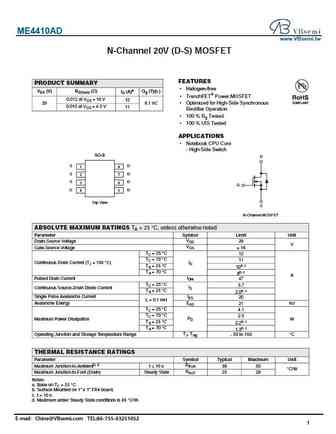
ME4410AD www.VBsemi.tw N-Channel 20V (D-S) MOSFET FEATURES PRODUCT SUMMARY Halogen-free VDS (V) RDS(on) ( ) ID (A)a Qg (Typ.) TrenchFET Power MOSFET 0.012 at VGS = 10 V 12 20 6.1 nC Optimized for High-Side Synchronous 0.015 at VGS = 4.5 V 11 Rectifier Operation 100 % Rg Tested 100 % UIS Tested APPLICATIONS Notebook CPU Core - High-Side Switch SO
vbza4410.pdf
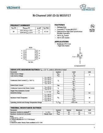
VBZA4410 www.VBsemi.com N-Channel 20V (D-S) MOSFET FEATURES PRODUCT SUMMARY Halogen-free VDS (V) RDS(on) ( ) ID (A)a Qg (Typ.) TrenchFET Power MOSFET 0.011 at VGS = 10 V 11 20 6.1 nC Optimized for High-Side Synchronous 0.015 at VGS = 4.5 V 9 Rectifier Operation 100 % Rg Tested 100 % UIS Tested APPLICATIONS Notebook CPU Core - High-Side Switch SO
irfr4105ztr.pdf
IRFR4105ZTR www.VBsemi.tw N-Channel 6 0-V (D-S) MOSFET FEATURES PRODUCT SUMMARY TrenchFET Power MOSFET VDS (V) rDS(on) ( ) ID (A)a Available 175 C Junction Temperature 0.025 at VGS = 10 V 35 RoHS* 60 0.030 at VGS = 4.5 V 30 COMPLIANT TO-252 D G Drain Connected to Tab G D S S Top View N-Channel MOSFET ABSOLUTE MAXIMUM RATINGS TC = 25 C, unless otherwise n
hm4410.pdf
HM4410 www.VBsemi.tw N-Channel 30-V (D-S) MOSFET FEATURES PRODUCT SUMMARY Halogen-free VDS (V) RDS(on) ( ) ID (A)a Qg (Typ.) TrenchFET Power MOSFET 0.008 at VGS = 10 V 13 30 6.1 nC Optimized for High-Side Synchronous 0.011 at VGS = 4.5 V 11 Rectifier Operation 100 % Rg Tested 100 % UIS Tested APPLICATIONS Notebook CPU Core - High-Side Switch SO
me4410.pdf
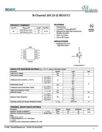
ME4410 www.VBsemi.tw N-Channel 20V (D-S) MOSFET FEATURES PRODUCT SUMMARY Halogen-free VDS (V) RDS(on) ( ) ID (A)a Qg (Typ.) TrenchFET Power MOSFET 0.012 at VGS = 10 V 12 20 6.1 nC Optimized for High-Side Synchronous 0.015 at VGS = 4.5 V 11 Rectifier Operation 100 % Rg Tested 100 % UIS Tested APPLICATIONS Notebook CPU Core - High-Side Switch SO-8
irlu3410p.pdf
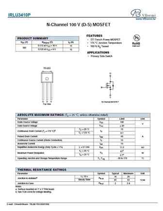
IRLU3410P www.VBsemi.tw N-Channel 100 V (D-S) MOSFET FEATURES PRODUCT SUMMARY DT-Trench Power MOSFET VDS (V) RDS(on) ( )ID (A) 175 C Junction Temperature 0.115 at VGS = 10 V 15 100 % Rg Tested 100 0.120 at VGS = 6 V 15 APPLICATIONS Primary Side Switch TO-251 D G S G D S N-Channel MOSFET Top View ABSOLUTE MAXIMUM RATINGS (TC = 25 C, unless otherwise
vba3410.pdf
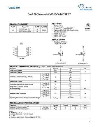
VBA3410 www.VBsemi.com Dual N-Channel 40-V (D-S) MOSFET FEATURES PRODUCT SUMMARY Halogen-free VDS (V) RDS(on) ( ) ID (A)a Qg (Typ.) TrenchFET Power MOSFET 0.010 at VGS = 10 V 12 40 5.9 nC Optimized for High-Side Synchronous 0.015 at VGS = 4.5 V 10 Rectifier Operation 100 % Rg Tested 100 % UIS Tested APPLICATIONS Notebook CPU Core - High-Side Swit
vba1410.pdf
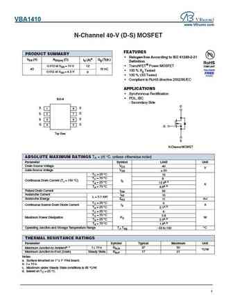
VBA1410 www.VBsemi.com N-Channel 40-V (D-S) MOSFET FEATURES PRODUCT SUMMARY Halogen-free According to IEC 61249-2-21 VDS (V) RDS(on) ( ) ID (A)d Qg (Typ.) Definition 0.012 at VGS = 10 V TrenchFET Power MOSFET 12 40 15 nC 100 % Rg Tested 0.012 at VGS = 4.5 V 9 100 % UIS Tested Compliant to RoHS directive 2002/95/EC APPLICATIONS Synchronous Re
vbza9410.pdf
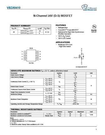
VBZA9410 www.VBsemi.com N-Channel 20V (D-S) MOSFET FEATURES PRODUCT SUMMARY Halogen-free VDS (V) RDS(on) ( ) ID (A)a Qg (Typ.) TrenchFET Power MOSFET 0.012 at VGS = 10 V 12 20 6.1 nC Optimized for High-Side Synchronous 0.015 at VGS = 4.5 V 9 Rectifier Operation 100 % Rg Tested 100 % UIS Tested APPLICATIONS Notebook CPU Core - High-Side Switch SO
irf7410tr.pdf
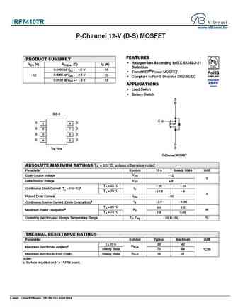
IRF7410TR www.VBsemi.tw P-Channel 12-V (D-S) MOSFET FEATURES PRODUCT SUMMARY Halogen-free According to IEC 61249-2-21 VDS (V) RDS(on) ( )ID (A) Definition 0.0050 at VGS = - 4.5 V - 16 TrenchFET Power MOSFET 0.0065 at VGS = - 2.5 V - 12 - 15 Compliant to RoHS Directive 2002/95/EC 0.0100 at VGS = - 1.8 V - 13 APPLICATIONS Load Switch Battery Switch S
vbe1410.pdf
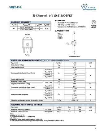
VBE1410 www.VBsemi.com N-Channel 4 0-V (D-S) MOSFET FEATURES PRODUCT SUMMARY TrenchFET Power MOSFET VDS (V) RDS(on) ( ) ID (A)a, e Qg (Typ) 100 % Rg and UIS Tested Compliant to RoHS Directive 2011/65/EU 0.013 at VGS = 10 V 55 40 42 nC 0.018 at VGS = 4.5 V 45 APPLICATIONS D OR-ing TO-252 Server DC/DC G D G S S Top View N-Channel MOSFET ABS
irfr3410tr.pdf
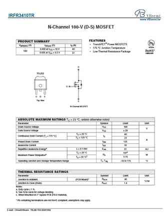
IRFR3410TR www.VBsemi.tw N-Channel 100-V (D-S) MOSFET FEATURES PRODUCT SUMMARY TrenchFET Power MOSFETS V(BR)DSS (V) rDS(on) ( )ID (A) Available 175 C Junction Temperature 0.030 at VGS = 10 V 40 RoHS* 100 Low Thermal Resistance Package 0.035 at VGS = 4.5 V 37 COMPLIANT D TO-252 G G D S Top View S N-Channel MOSFET ABSOLUTE MAXIMUM RATINGS TC = 25 C, unl
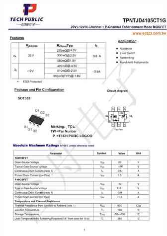
tpnts4101pt1g.pdf
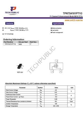
TPNTS4 1 01 PT1 G P-Channel Enhancement-Mode MOS FETs www.sot23.com.tw Features Applications (typ) @VGS =4.5V. -20V, -2.3A, RDS(ON) =100m Battery protection RDS(ON) = 125m (typ) @VGS = 2.5V. Load switch Power management SOT-323 package. Ordering Information Part Number Qty per Reel Reel Size TPNTS4101PT1G 3000 7 D S G SOT-323 Absolute Maximum Ratings (TA=
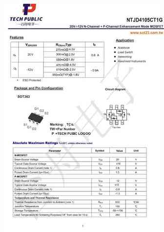
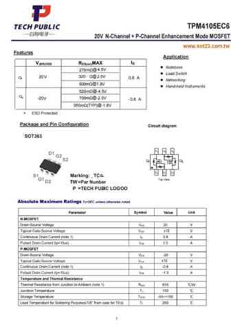
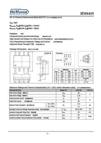
hm4410b.pdf
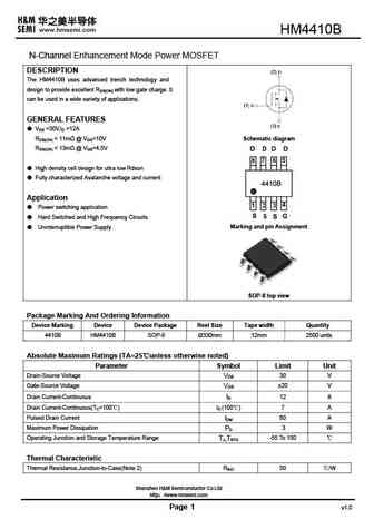
HM4410B N-Channel Enhancement Mode Power MOSFET DESCRIPTION The HM4410B uses advanced trench technology and design to provide excellent RDS(ON) with low gate charge. It can be used in a wide variety of applications. GENERAL FEATURES VDS =30V,ID =12A RDS(ON)
hm4410a.pdf
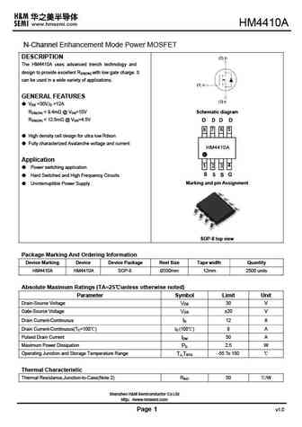
HM4410A N-Channel Enhancement Mode Power MOSFET DESCRIPTION The HM4410A uses advanced trench technology and design to provide excellent RDS(ON) with low gate charge. It can be used in a wide variety of applications. GENERAL FEATURES VDS =30V,ID =12A RDS(ON)
irfb4410zg.pdf
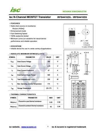
isc N-Channel MOSFET Transistor IRFB4410ZG IIRFB4410ZG FEATURES Static drain-source on-resistance RDS(on) 9.0m Enhancement mode Fast Switching Speed 100% avalanche tested Minimum Lot-to-Lot variations for robust device performance and reliable operation DESCRITION reliable device for use in a wide variety of applications ABSOLUTE MAXIMUM RATINGS(T =25 )
irfr3410.pdf
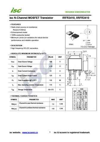
isc N-Channel MOSFET Transistor IRFR3410, IIRFR3410 FEATURES Static drain-source on-resistance RDS(on) 39m Enhancement mode 100% avalanche tested Minimum Lot-to-Lot variations for robust device performance and reliable operation DESCRITION High frequency DC-DC converters ABSOLUTE MAXIMUM RATINGS(T =25 ) a SYMBOL PARAMETER VALUE UNIT V Drain-Source Voltage 1
irfu4105.pdf
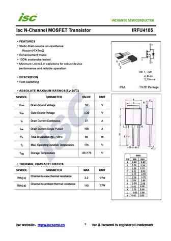
isc N-Channel MOSFET Transistor IRFU4105 FEATURES Static drain-source on-resistance RDS(on) 45m Enhancement mode 100% avalanche tested Minimum Lot-to-Lot variations for robust device performance and reliable operation DESCRITION Fast Switching ABSOLUTE MAXIMUM RATINGS(T =25 ) a SYMBOL PARAMETER VALUE UNIT V Drain-Source Voltage 55 V DSS V Gate-Source Volt
dki04103.pdf
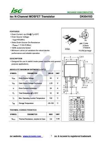
isc N-Channel MOSFET Transistor DKI04103 FEATURES Drain Current I =29A@ T =25 D C Drain Source Voltage- V =40V(Min) DSS Static Drain-Source On-Resistance R = 11.8m (Max) DS(on) 100% avalanche tested Minimum Lot-to-Lot variations for robust device performance and reliable operation DESCRIPTION Designed for use in switch mode power supplies and general purpos
irfu4105z.pdf
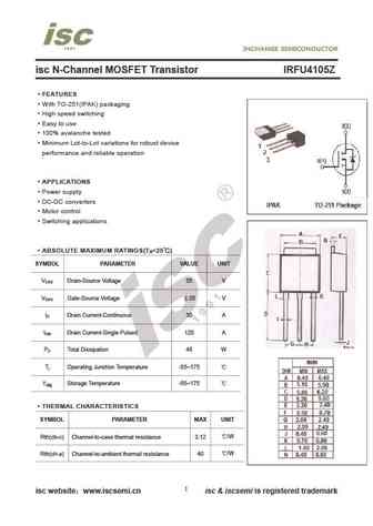
isc N-Channel MOSFET Transistor IRFU4105Z FEATURES With TO-251(IPAK) packaging High speed switching Easy to use 100% avalanche tested Minimum Lot-to-Lot variations for robust device performance and reliable operation APPLICATIONS Power supply DC-DC converters Motor control Switching applications ABSOLUTE MAXIMUM RATINGS(T =25 ) a SYMBOL PARAMETER VALUE U
aod4102.pdf
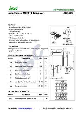
isc N-Channel MOSFET Transistor AOD4102 FEATURES Drain Current I = 19A@ T =25 D C Drain Source Voltage- V =30V(Min) DSS Static Drain-Source On-Resistance R =37m (Max) DS(on) 100% avalanche tested Minimum Lot-to-Lot variations for robust device performance and reliable operation DESCRIPTION Designed for use in switch mode power supplies and general purpose a
irfs4410z.pdf

Isc N-Channel MOSFET Transistor IRFS4410Z FEATURES With To-263(D2PAK) package Low input capacitance and gate charge Low gate input resistance 100% avalanche tested Minimum Lot-to-Lot variations for robust device performance and reliable operation APPLICATIONS Switching applications ABSOLUTE MAXIMUM RATINGS(T =25 ) a SYMBOL PARAMETER VALUE UNIT V Drain-Source Vol
2sk4101ls.pdf
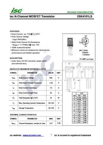
isc N-Channel MOSFET Transistor 2SK4101LS FEATURES Drain Current I = 7.0A@ T =25 D C Drain Source Voltage V = 650V(Min) DSS Static Drain-Source On-Resistance R = 1.1 (Max) @ V = 10V DS(on) GS 100% avalanche tested Minimum Lot-to-Lot variations for robust device performance and reliable operation DESCRIPTION motor drive, DC-DC converter, power switch and sole
mj410.pdf
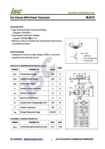
isc Silicon NPN Power Transistor MJ410 DESCRIPTION High Collector-Emitter Sustaining Voltage- V = 200V(Min.) CEO(SUS) Low Collector Saturation Voltage- V )= 0.8V(Max)@ I = 1A CE(sat C Minimum Lot-to-Lot variations for robust device performance and reliable operation APPLICATIONS Designed for medium to high voltage inverters, converters, regulators and switching circuits.
buf410a.pdf
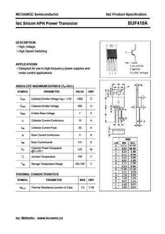
INCHANGE Semiconductor isc Product Specification isc Silicon NPN Power Transistor BUF410A DESCRIPTION High Voltage High Speed Switching APPLICATIONS Designed for use in high-frequency power supplies and motor control applications. ABSOLUTE MAXIMUM RATINGS (Ta=25 ) SYMBOL PARAMETER VALUE UNIT VCEV Collector-Emitter Voltage VBE= -1.5V 1000 V VCEO Collector-Emitter Vo
2sc4106.pdf
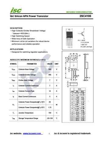
isc Silicon NPN Power Transistor 2SC4106 DESCRIPTION High Collector-Emitter Breakdown Voltage V = 400V(Min.) (BR)CEO High Switching Speed Wide Area of Safe Operation Minimum Lot-to-Lot variations for robust device performance and reliable operation APPLICATIONS Designed for switching regulator applications ABSOLUTE MAXIMUM RATINGS(Ta=25 ) SYMBOL PARAMETER VALUE UNIT V
irfs4410.pdf
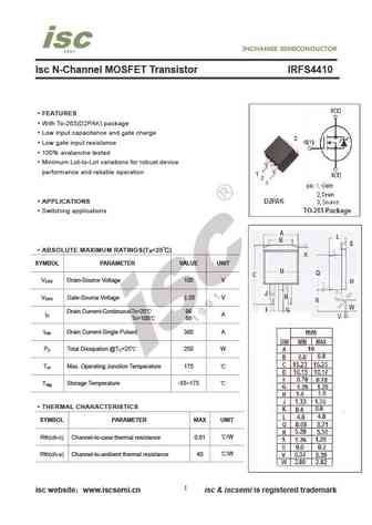
Isc N-Channel MOSFET Transistor IRFS4410 FEATURES With To-263(D2PAK) package Low input capacitance and gate charge Low gate input resistance 100% avalanche tested Minimum Lot-to-Lot variations for robust device performance and reliable operation APPLICATIONS Switching applications ABSOLUTE MAXIMUM RATINGS(T =25 ) a SYMBOL PARAMETER VALUE UNIT V Drain-Source Volt
irfr4105z.pdf
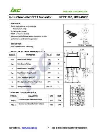
isc N-Channel MOSFET Transistor IRFR4105Z, IIRFR4105Z FEATURES Static drain-source on-resistance RDS(on) 24.5m Enhancement mode 100% avalanche tested Minimum Lot-to-Lot variations for robust device performance and reliable operation DESCRITION High Speed Power Switching ABSOLUTE MAXIMUM RATINGS(T =25 ) a SYMBOL PARAMETER VALUE UNIT V Drain-Source Voltage 55
2sd1410.pdf
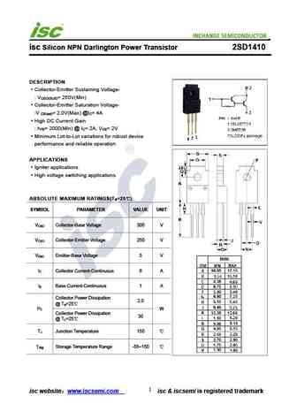
isc Silicon NPN Darlington Power Transistor 2SD1410 DESCRIPTION Collector-Emitter Sustaining Voltage- V = 250V(Min) CEO(SUS) Collector-Emitter Saturation Voltage- V = 2.0V(Max) @I = 4A CE(sat) C High DC Current Gain h = 2000(Min) @ I = 2A, V = 2V FE C CE Minimum Lot-to-Lot variations for robust device performance and reliable operation APPLICATIONS Igniter applicati
2sc4108.pdf
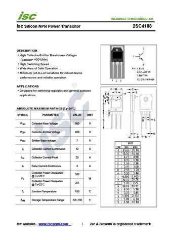
isc Silicon NPN Power Transistor 2SC4108 DESCRIPTION High Collector-Emitter Breakdown Voltage- V = 400V(Min) (BR)CEO High Switching Speed Wide Area of Safe Operation Minimum Lot-to-Lot variations for robust device performance and reliable operation APPLICATIONS Designed for switching regulator and general purpose applications. ABSOLUTE MAXIMUM RATINGS(T =25 ) a SYMBO
irfp4410z.pdf
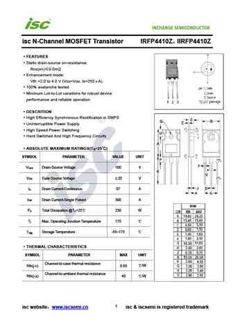
isc N-Channel MOSFET Transistor IRFP4410Z IIRFP4410Z FEATURES Static drain-source on-resistance RDS(on) 9.0m Enhancement mode Vth =2.0 to 4.0 V (VDS=VGS, ID=250 A) 100% avalanche tested Minimum Lot-to-Lot variations for robust device performance and reliable operation DESCRITION High Efficiency Synchronous Rectification in SMPS Uninterruptible Power Supply
2sc4107.pdf
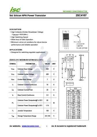
isc Silicon NPN Power Transistor 2SC4107 DESCRIPTION High Collector-Emitter Breakdown Voltage V = 400V(Min.) (BR)CEO High Switching Speed Wide Area of Safe Operation Minimum Lot-to-Lot variations for robust device performance and reliable operation APPLICATIONS Designed for switching regulator applications ABSOLUTE MAXIMUM RATINGS(Ta=25 ) SYMBOL PARAMETER VALUE UNIT V
2sk1410.pdf
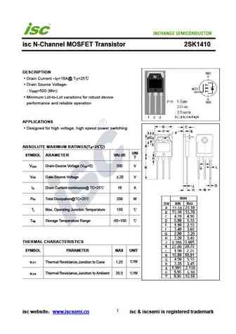
isc N-Channel MOSFET Transistor 2SK1410 DESCRIPTION Drain Current I =16A@ T =25 D C Drain Source Voltage- V =500 (Min) DSS Minimum Lot-to-Lot variations for robust device performance and reliable operation APPLICATIONS Designed for high voltage, high speed power switching ABSOLUTE MAXIMUM RATINGS(T =25 ) a UNI SYMBOL ARAMETER VALUE T V Drain-Source Voltage (V =
2sc4109.pdf
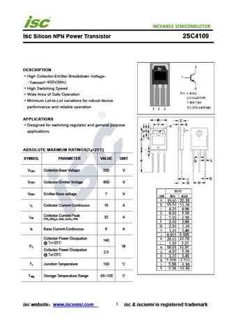
isc Silicon NPN Power Transistor 2SC4109 DESCRIPTION High Collector-Emitter Breakdown Voltage- V = 400V(Min) (BR)CEO High Switching Speed Wide Area of Safe Operation Minimum Lot-to-Lot variations for robust device performance and reliable operation APPLICATIONS Designed for switching regulator and general purpose applications. ABSOLUTE MAXIMUM RATINGS(T =25 ) a SYMBO
buf410.pdf
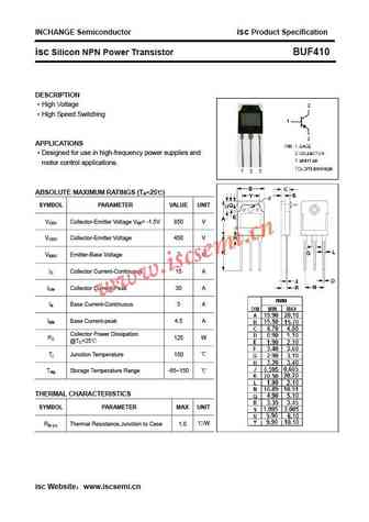
INCHANGE Semiconductor isc Product Specification isc Silicon NPN Power Transistor BUF410 DESCRIPTION High Voltage High Speed Switching APPLICATIONS Designed for use in high-frequency power supplies and motor control applications. ABSOLUTE MAXIMUM RATINGS (Ta=25 ) SYMBOL PARAMETER VALUE UNIT VCEV Collector-Emitter Voltage VBE= -1.5V 850 V VCEO Collector-Emitter Volt
irlr3410.pdf
isc N-Channel MOSFET Transistor IRLR3410, IIRLR3410 FEATURES Static drain-source on-resistance RDS(on) 105m Enhancement mode 100% avalanche tested Minimum Lot-to-Lot variations for robust device performance and reliable operation DESCRITION Fast Switching ABSOLUTE MAXIMUM RATINGS(T =25 ) a SYMBOL PARAMETER VALUE UNIT V Drain-Source Voltage 100 V DSS V Gat
irf4104s.pdf

Isc N-Channel MOSFET Transistor IRF4104S FEATURES With To-263(D2PAK) package Low input capacitance and gate charge Low gate input resistance 100% avalanche tested Minimum Lot-to-Lot variations for robust device performance and reliable operation APPLICATIONS Switching applications ABSOLUTE MAXIMUM RATINGS(T =25 ) a SYMBOL PARAMETER VALUE UNIT V Drain-Source Volt
2sk4100ls.pdf

isc N-Channel MOSFET Transistor 2SK4100LS FEATURES Drain Current I = 6.0A@ T =25 D C Drain Source Voltage V = 650V(Min) DSS Static Drain-Source On-Resistance R = 1.35 (Max) @ V = 10V DS(on) GS 100% avalanche tested Minimum Lot-to-Lot variations for robust device performance and reliable operation DESCRIPTION motor drive, DC-DC converter, power switch and sol
aow410.pdf
isc N-Channel MOSFET Transistor AOW410 FEATURES Drain Current I = 150A@ T =25 D C Drain Source Voltage- V = 100V(Min) DSS Static Drain-Source On-Resistance R = 6.5m (Max) DS(on) 100% avalanche tested Minimum Lot-to-Lot variations for robust device performance and reliable operation DESCRITION Be suitable for synchronous rectification for server and gene
irfsl4410.pdf
isc N-Channel MOSFET Transistor IRFSL4410 FEATURES Static drain-source on-resistance RDS(on) 10m Enhancement mode Fast Switching Speed 100% avalanche tested Minimum Lot-to-Lot variations for robust device performance and reliable operation DESCRITION reliable device for use in a wide variety of applications ABSOLUTE MAXIMUM RATINGS(T =25 ) a SYMBOL PARAME
irfr4105.pdf
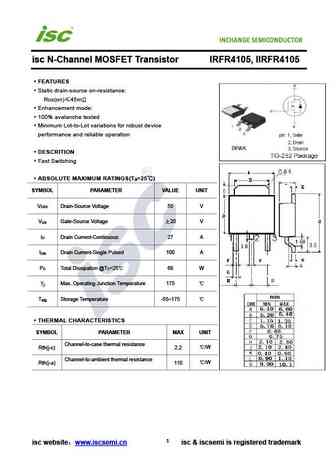
isc N-Channel MOSFET Transistor IRFR4105, IIRFR4105 FEATURES Static drain-source on-resistance RDS(on) 45m Enhancement mode 100% avalanche tested Minimum Lot-to-Lot variations for robust device performance and reliable operation DESCRITION Fast Switching ABSOLUTE MAXIMUM RATINGS(T =25 ) a SYMBOL PARAMETER VALUE UNIT V Drain-Source Voltage 55 V DSS V Gate-
irf4104.pdf
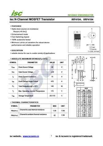
INCHANGE Semiconductor isc N-Channel MOSFET Transistor IRF4104 IIRF4104 FEATURES Static drain-source on-resistance RDS(on) 5.5m Enhancement mode Fast Switching Speed 100% avalanche tested Minimum Lot-to-Lot variations for robust device performance and reliable operation DESCRITION reliable device for use in a wide variety of applications ABSOLUTE MAXIMUM R
irfi4410z.pdf
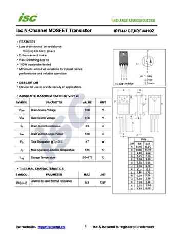
isc N-Channel MOSFET Transistor IRFI4410Z,IIRFI4410Z FEATURES Low drain-source on-resistance RDS(on) 9.3m (max) Enhancement mode Fast Switching Speed 100% avalanche tested Minimum Lot-to-Lot variations for robust device performance and reliable operation DESCRITION Device for use in a wide variety of applications ABSOLUTE MAXIMUM RATINGS(T =25 ) a SYMBOL
2sk4108.pdf
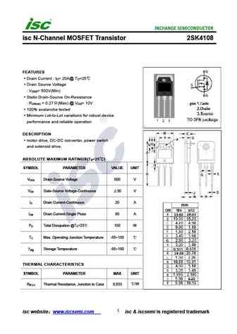
isc N-Channel MOSFET Transistor 2SK4108 FEATURES Drain Current I = 20A@ T =25 D C Drain Source Voltage V = 500V(Min) DSS Static Drain-Source On-Resistance R = 0.27 (Max) @ V = 10V DS(on) GS 100% avalanche tested Minimum Lot-to-Lot variations for robust device performance and reliable operation DESCRIPTION motor drive, DC-DC converter, power switch and soleno
irfb4410.pdf
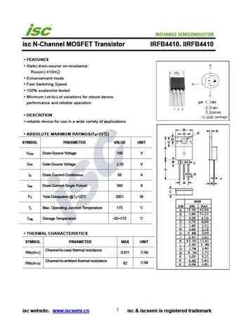
INCHANGE Semiconductor isc N-Channel MOSFET Transistor IRFB4410 IIRFB4410 FEATURES Static drain-source on-resistance RDS(on) 10m Enhancement mode Fast Switching Speed 100% avalanche tested Minimum Lot-to-Lot variations for robust device performance and reliable operation DESCRITION reliable device for use in a wide variety of applications ABSOLUTE MAXIMU
aoi4102.pdf
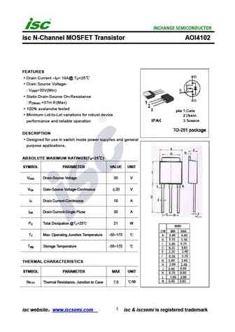
isc N-Channel MOSFET Transistor AOI4102 FEATURES Drain Current I = 19A@ T =25 D C Drain Source Voltage- V =30V(Min) DSS Static Drain-Source On-Resistance R =37m (Max) DS(on) 100% avalanche tested Minimum Lot-to-Lot variations for robust device performance and reliable operation DESCRIPTION Designed for use in switch mode power supplies and general purpose a
aot410l.pdf
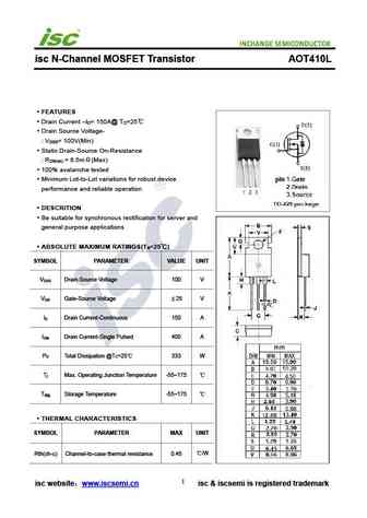
isc N-Channel MOSFET Transistor AOT410L FEATURES Drain Current I = 150A@ T =25 D C Drain Source Voltage- V = 100V(Min) DSS Static Drain-Source On-Resistance R = 6.5m (Max) DS(on) 100% avalanche tested Minimum Lot-to-Lot variations for robust device performance and reliable operation DESCRITION Be suitable for synchronous rectification for server and gen
irfr5410.pdf
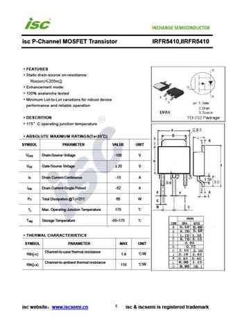
isc P-Channel MOSFET Transistor IRFR5410,IIRFR5410 FEATURES Static drain-source on-resistance RDS(on) 205m Enhancement mode 100% avalanche tested Minimum Lot-to-Lot variations for robust device performance and reliable operation DESCRITION 175 C operating junction temperature ABSOLUTE MAXIMUM RATINGS(T =25 ) a SYMBOL PARAMETER VALUE UNIT V Drain-Source Vol
irfu4104.pdf

isc N-Channel MOSFET Transistor IRFU4104 FEATURES With TO-251(IPAK) packaging High speed switching Easy to use 100% avalanche tested Minimum Lot-to-Lot variations for robust device performance and reliable operation APPLICATIONS Power supply DC-DC converters Motor control Switching applications ABSOLUTE MAXIMUM RATINGS(T =25 ) a SYMBOL PARAMETER VALUE UN
2sc4105.pdf
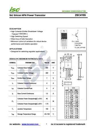
isc Silicon NPN Power Transistor 2SC4105 DESCRIPTION High Collector-Emitter Breakdown Voltage V = 400V(Min.) (BR)CEO High Switching Speed Wide Area of Safe Operation Minimum Lot-to-Lot variations for robust device performance and reliable operation APPLICATIONS Designed for switching regulator applications ABSOLUTE MAXIMUM RATINGS(Ta=25 ) SYMBOL PARAMETER VALUE UNIT V
irlu3410.pdf

isc N-Channel MOSFET Transistor IRLU3410 FEATURES With TO-251(IPAK) packaging High speed switching Easy to use 100% avalanche tested Minimum Lot-to-Lot variations for robust device performance and reliable operation APPLICATIONS Power supply DC-DC converters Motor control Switching applications ABSOLUTE MAXIMUM RATINGS(T =25 ) a SYMBOL PARAMETER VALUE UN
irfb4410z.pdf

INCHANGE Semiconductor isc N-Channel MOSFET Transistor IRFB4410Z IIRFB4410Z FEATURES Static drain-source on-resistance RDS(on) 9.0m Enhancement mode Fast Switching Speed 100% avalanche tested Minimum Lot-to-Lot variations for robust device performance and reliable operation DESCRITION reliable device for use in a wide variety of applications ABSOLUTE MAXIM
ipp410n30n.pdf
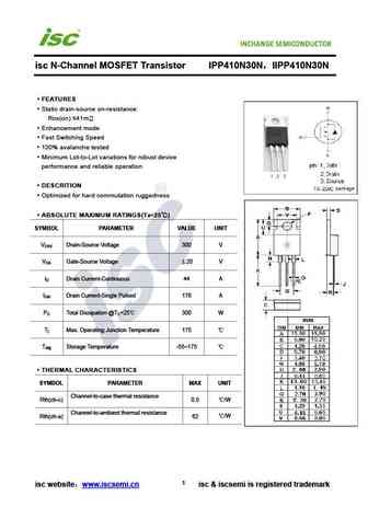
isc N-Channel MOSFET Transistor IPP410N30N IIPP410N30N FEATURES Static drain-source on-resistance RDS(on) 41m Enhancement mode Fast Switching Speed 100% avalanche tested Minimum Lot-to-Lot variations for robust device performance and reliable operation DESCRITION Optimized for hard commutation ruggedness ABSOLUTE MAXIMUM RATINGS(T =25 ) a SYMBOL PARAMET
aob410l.pdf
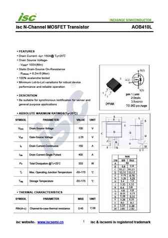
isc N-Channel MOSFET Transistor AOB410L FEATURES Drain Current I = 150A@ T =25 D C Drain Source Voltage- V = 100V(Min) DSS Static Drain-Source On-Resistance R = 6.2m (Max) DS(on) 100% avalanche tested Minimum Lot-to-Lot variations for robust device performance and reliable operation DESCRITION Be suitable for synchronous rectification for server and gen
buf410ai.pdf
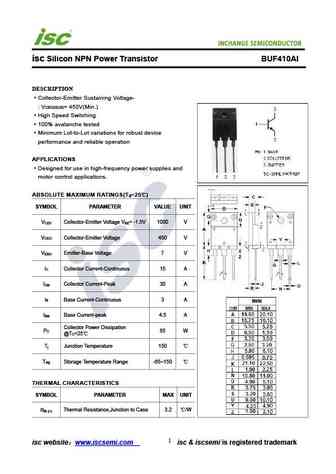
isc Silicon NPN Power Transistor BUF410AI DESCRIPTION Collector-Emitter Sustaining Voltage- V = 450V(Min.) CEO(SUS) High Speed Switching 100% avalanche tested Minimum Lot-to-Lot variations for robust device performance and reliable operation APPLICATIONS Designed for use in high-frequency power supplies and motor control applications. ABSOLUTE MAXIMUM RATINGS(T =25 )
buf410i.pdf
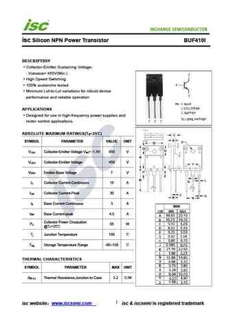
isc Silicon NPN Power Transistor BUF410I DESCRIPTION Collector-Emitter Sustaining Voltage- V = 450V(Min.) CEO(SUS) High Speed Switching 100% avalanche tested Minimum Lot-to-Lot variations for robust device performance and reliable operation APPLICATIONS Designed for use in high-frequency power supplies and motor control applications. ABSOLUTE MAXIMUM RATINGS(T =25 ) a
irfu3410.pdf

isc N-Channel MOSFET Transistor IRFU3410 FEATURES With TO-251(IPAK) packaging High speed switching Easy to use 100% avalanche tested Minimum Lot-to-Lot variations for robust device performance and reliable operation APPLICATIONS Power supply DC-DC converters Motor control Switching applications ABSOLUTE MAXIMUM RATINGS(T =25 ) a SYMBOL PARAMETER VALUE UN
irfr4104.pdf
isc N-Channel MOSFET Transistor IRFR4104, IIRFR4104 FEATURES Static drain-source on-resistance RDS(on) 5.5m Enhancement mode 100% avalanche tested Minimum Lot-to-Lot variations for robust device performance and reliable operation DESCRITION Fast switching ABSOLUTE MAXIMUM RATINGS(T =25 ) a SYMBOL PARAMETER VALUE UNIT V Drain-Source Voltage 40 V DSS V Gate
irfsl4410z.pdf
INCHANGE Semiconductor isc N-Channel MOSFET Transistor IRFSL4410Z FEATURES Static drain-source on-resistance RDS(on) 9.0m Enhancement mode Fast Switching Speed 100% avalanche tested Minimum Lot-to-Lot variations for robust device performance and reliable operation DESCRITION reliable device for use in a wide variety of applications ABSOLUTE MAXIMUM RATINGS(T
irfu5410.pdf
isc P-Channel MOSFET Transistor IRFU5410 FEATURES Static drain-source on-resistance RDS(on) 205m Enhancement mode 100% avalanche tested Minimum Lot-to-Lot variations for robust device performance and reliable operation DESCRITION 175 C operating junction temperature ABSOLUTE MAXIMUM RATINGS(T =25 ) a SYMBOL PARAMETER VALUE UNIT V Drain-Source Voltage -100
ap3410mi.pdf
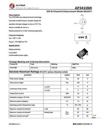
AP3410MI 30V N-Channel Enhancement Mode MOSFET Description The AP3410MI uses advanced trench technology to provide excellent R , low gate charge and DS(ON) operation with gate voltages as low as 4.5V. This device is suitable for use as a Battery protection or in other Switching application. General Features V = 30V I =6A DS D R
Otros transistores... 40974 , 40975 , 40976 , 40977 , 40979 , 40980 , 40TA045 , 40TA045D , S8550 , 41008 , 41008A , 41009 , 41009A , 41010 , 41012 , 41013 , 41024 .


Liste
Recientemente añadidas las descripciónes de los transistores:
BJT: GA1A4M | SBT42 | 2SA200-Y | 2SA200-O | 2SD882-Q | 2SD882-P | 2SD882-E | 2SC945-L | 2SC945-H | 2SC4226-R23 | 2SC3357-F | 2SC3357-E | 2SC3356-R26 | 2SC3356-R24 | 2SC3356-R23 | 2SB772-Q | 2SB772-P | 2SB772-E | 2SA1015-L | 2SA1015-H | HSS8550
Popular searches
2sa816 | 2sc897 datasheet | 2sd389 | mp41 transistor | nkt275 datasheet | 2sd947 | a763 transistor | fhp40n20