C64 Equivalente. Reemplazo. Hoja de especificaciones. Principales características
Número de Parte: C64
Material: Si
Polaridad de transistor: NPN
ESPECIFICACIONES MÁXIMAS
Disipación total del dispositivo (Pc): 0.36 W
Tensión colector-base (Vcb): 50 V
Tensión colector-emisor (Vce): 35 V
Temperatura operativa máxima (Tj): 175 °C
CARACTERÍSTICAS ELÉCTRICAS
Transición de frecuencia (fT): 250 MHz
Capacitancia de salida (Cc): 3 pF
Ganancia de corriente contínua (hFE): 65
Encapsulados: TO18
Búsqueda de reemplazo de C64
- Selecciónⓘ de transistores por parámetros
C64 datasheet
0.1. Size:117K 1
ntmfs5c646nlt3g.pdf 

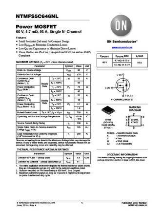
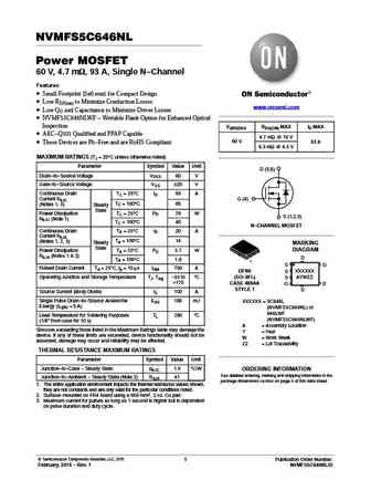
NTMFS5C646NL Power MOSFET 60 V, 4.7 mW, 93 A, Single N-Channel Features Small Footprint (5x6 mm) for Compact Design Low RDS(on) to Minimize Conduction Losses www.onsemi.com Low QG and Capacitance to Minimize Driver Losses These Devices are Pb-Free, Halogen Free/BFR Free and are RoHS Compliant V(BR)DSS RDS(ON) MAX ID MAX 4.7 mW @ 10 V MAXIMUM RATINGS (TJ = 25 C unles
0.2. Size:118K 1
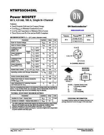
ntmfs5c645nlt3g.pdf

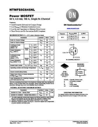
NTMFS5C645NL Power MOSFET 60 V, 4.0 mW, 100 A, Single N-Channel Features Small Footprint (5x6 mm) for Compact Design Low RDS(on) to Minimize Conduction Losses www.onsemi.com Low QG and Capacitance to Minimize Driver Losses These Devices are Pb-Free and are RoHS Compliant V(BR)DSS RDS(ON) MAX ID MAX MAXIMUM RATINGS (TJ = 25 C unless otherwise noted) 4.0 mW @ 10 V 60
0.3. Size:76K 1
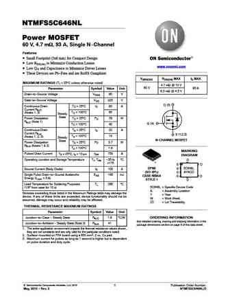
ntmfs5c646nlt1g.pdf
NTMFS5C646NL Power MOSFET 60 V, 4.7 mW, 93 A, Single N-Channel Features Small Footprint (5x6 mm) for Compact Design Low RDS(on) to Minimize Conduction Losses www.onsemi.com Low QG and Capacitance to Minimize Driver Losses These Devices are Pb-Free, Halogen Free/BFR Free and are RoHS Compliant V(BR)DSS RDS(ON) MAX ID MAX 4.7 mW @ 10 V MAXIMUM RATINGS (TJ = 25 C unles
0.4. Size:186K 1
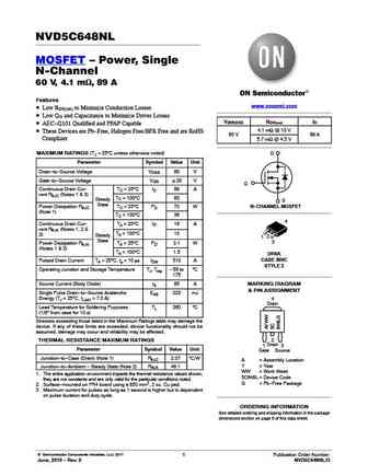
nvd5c648nl.pdf
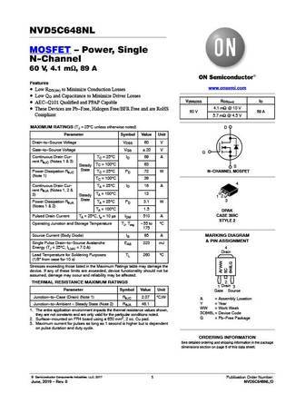
NVD5C648NL MOSFET Power, Single N-Channel 60 V, 4.1 mW, 89 A Features www.onsemi.com Low RDS(on) to Minimize Conduction Losses Low QG and Capacitance to Minimize Driver Losses V(BR)DSS RDS(on) ID AEC-Q101 Qualified and PPAP Capable 4.1 mW @ 10 V These Devices are Pb-Free, Halogen Free/BFR Free and are RoHS 60 V 89 A Compliant 5.7 mW @ 4.5 V MAXIMUM RATINGS (TJ
0.5. Size:114K 1
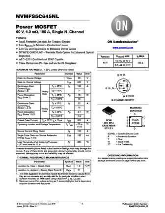
ntmfs5c645nlt1g.pdf
NTMFS5C645NL Power MOSFET 60 V, 4.0 mW, 100 A, Single N-Channel Features Small Footprint (5x6 mm) for Compact Design Low RDS(on) to Minimize Conduction Losses www.onsemi.com Low QG and Capacitance to Minimize Driver Losses These Devices are Pb-Free and are RoHS Compliant V(BR)DSS RDS(ON) MAX ID MAX MAXIMUM RATINGS (TJ = 25 C unless otherwise noted) 4.0 mW @ 10 V 60
0.6. Size:448K 1
ao6414 mc6414.pdf
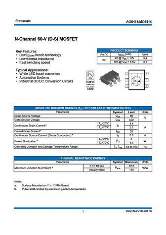
Freescale AO6414/ MC6414 N-Channel 60-V (D-S) MOSFET PRODUCT SUMMARY Key Features rDS(on) (m ) VDS (V) ID(A) Low r trench technology DS(on) 92 @ VGS = 10V 3.4 Low thermal impedance 60 107 @ VGS = 4.5V 3.1 Fast switching speed Typical Applications White LED boost converters Automotive Systems Industrial DC/DC Conversion Circuits ABSOLUTE MAX
0.7. Size:116K motorola
bc636 bc638 bc640.pdf
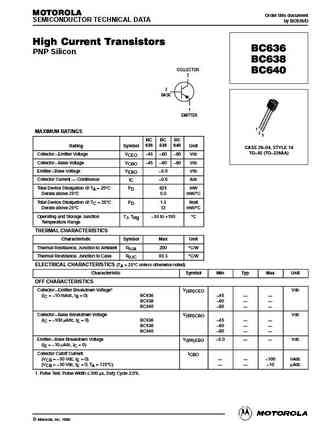
MOTOROLA Order this document SEMICONDUCTOR TECHNICAL DATA by BC636/D High Current Transistors BC636 PNP Silicon BC638 COLLECTOR BC640 2 3 BASE 1 EMITTER 1 MAXIMUM RATINGS 2 3 BC BC BC 636 638 640 Rating Symbol Unit CASE 29 04, STYLE 14 TO 92 (TO 226AA) Collector Emitter Voltage VCEO 45 60 80 Vdc Collector Base Voltage VCBO 45 60 80 Vdc Emitt
0.10. Size:136K philips
bc640 bcp53 bcx53.pdf
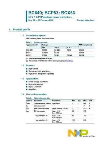
BC640; BCP53; BCX53 80 V, 1 A PNP medium power transistors Rev. 08 22 February 2008 Product data sheet 1. Product profile 1.1 General description PNP medium power transistor series. Table 1. Product overview Type number[1] Package NPN complement NXP JEITA JEDEC BC640[2] SOT54 SC-43A TO-92 BC639 BCP53 SOT223 SC-73 - BCP56 BCX53 SOT89 SC-62 TO-243 BCX56 [1] Valid for all available
0.11. Size:49K philips
bc636 bc638 bc640 3.pdf
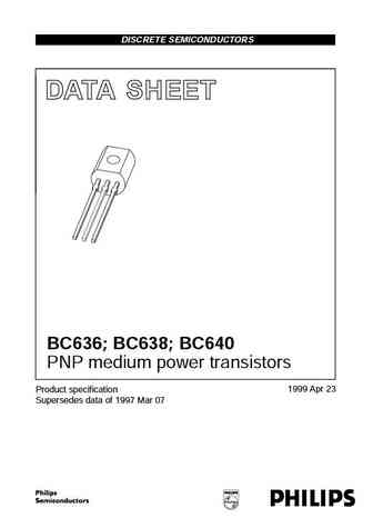
DISCRETE SEMICONDUCTORS DATA SHEET book, halfpage M3D186 BC636; BC638; BC640 PNP medium power transistors 1999 Apr 23 Product specification Supersedes data of 1997 Mar 07 Philips Semiconductors Product specification PNP medium power transistors BC636; BC638; BC640 FEATURES PINNING High current (max. 1 A) PIN DESCRIPTION Low voltage (max. 80 V). 1 base 2 collector APPLI
0.14. Size:241K fairchild semi
fdc642p f085.pdf
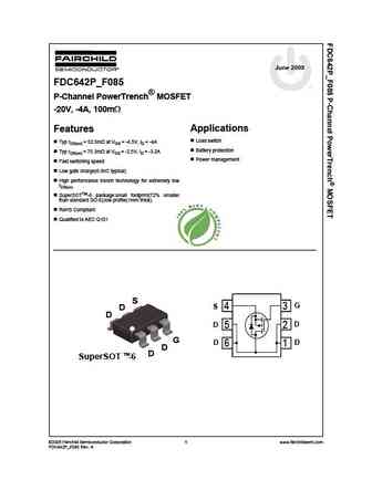
June 2009 FDC642P_F085 P-Channel PowerTrench MOSFET -20V, -4A, 100m Applications Features Load switch Typ rDS(on) = 52.5m at VGS = -4.5V, ID = -4A Battery protection Typ rDS(on) = 75.3m at VGS = -2.5V, ID = -3.2A Power management Fast switching speed Low gate charge(6.9nC typical) High performance trench technology for extremely low rDS(on) SuperSOTTM-6
0.15. Size:76K fairchild semi
fdc6401n.pdf
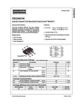
October 2001 FDC6401N Dual N-Channel 2.5V Specified PowerTrench MOSFET General Description Features This Dual N-Channel MOSFET has been designed 3.0 A, 20 V. RDS(ON) = 70 m @ VGS = 4.5 V specifically to improve the overall efficiency of DC/DC RDS(ON) = 95 m @ VGS = 2.5 V converters using either synchronous or conventional switching PWM controllers. It has been optimiz
0.16. Size:76K fairchild semi
fdc640p f095.pdf
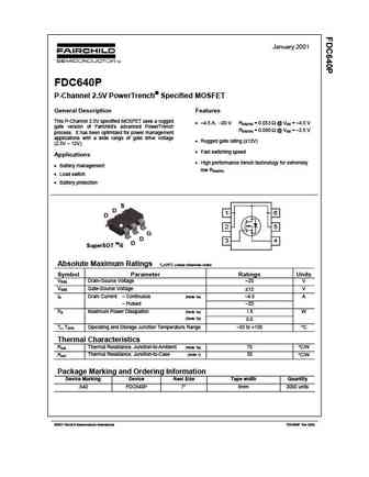
January 2001 FDC640P P-Channel 2.5V PowerTrench Specified MOSFET General Description Features This P-Channel 2.5V specified MOSFET uses a rugged 4.5 A, 20 V RDS(ON) = 0.053 @ VGS = 4.5 V gate version of Fairchild s advanced PowerTrench RDS(ON) = 0.080 @ VGS = 2.5 V process. It has been optimized for power management applications with a wide r
0.18. Size:78K fairchild semi
fdc640p.pdf

January 2001 FDC640P P-Channel 2.5V PowerTrench Specified MOSFET General Description Features This P-Channel 2.5V specified MOSFET uses a rugged 4.5 A, 20 V RDS(ON) = 0.053 @ VGS = 4.5 V gate version of Fairchild s advanced PowerTrench RDS(ON) = 0.080 @ VGS = 2.5 V process. It has been optimized for power management applications with a wide r
0.19. Size:266K fairchild semi
fdc642p.pdf
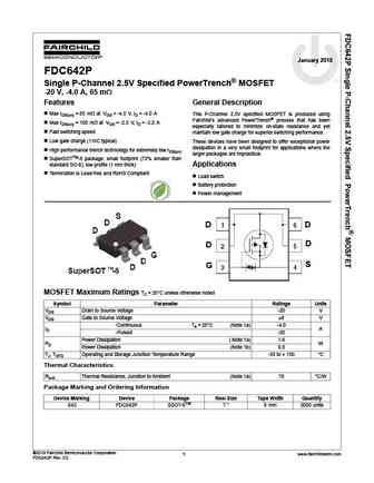
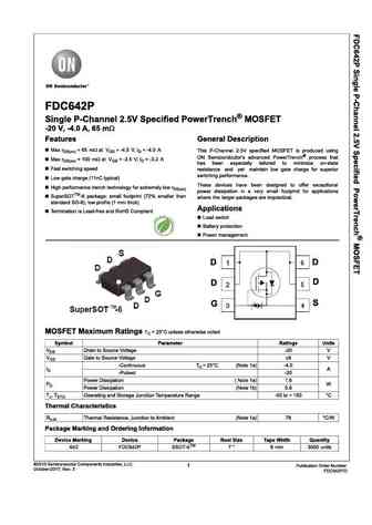
January 2010 FDC642P Single P-Channel 2.5V Specified PowerTrench MOSFET -20 V, -4.0 A, 65 m Features General Description Max rDS(on) = 65 m at VGS = -4.5 V, ID = -4.0 A This P-Channel 2.5V specified MOSFET is produced using Fairchild s advanced PowerTrench process that has been Max rDS(on) = 100 m at VGS = -2.5 V, ID = -3.2 A especially tailored to minimize on-state
0.20. Size:38K fairchild semi
bc636 bc638 bc640.pdf
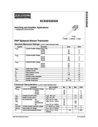
BC636/638/640 Switching and Amplifier Applications Complement to BC635/637/639 TO-92 1 1. Emitter 2. Collector 3. Base PNP Epitaxial Silicon Transistor Absolute Maximum Ratings Ta=25 C unless otherwise noted Symbol Parameter Value Units VCER Collector-Emitter Voltage at RBE=1K BC636 -45 V BC638 -60 V BC640 -100 V VCES Collector-Emitter Voltage BC636 -45 V BC6
0.21. Size:106K fairchild semi
bc640.pdf
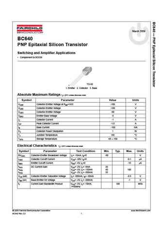
March 2009 BC640 PNP Epitaxial Silicon Transistor Switching and Amplifier Applications Complement to BC639 TO-92 1 1. Emitter 2. Collector 3. Base Absolute Maximum Ratings Ta = 25 C unless otherwise noted Symbol Parameter Value Units VCER Collector-Emitter Voltage at RBE=1K -100 V VCES Collector-Emitter Voltage -100 V VCEO Collector-Emitter Voltage -80 V VEBO Emitter-Base Vo
0.22. Size:136K nxp
bc640 bcp53 bcx53.pdf

BC640; BCP53; BCX53 80 V, 1 A PNP medium power transistors Rev. 08 22 February 2008 Product data sheet 1. Product profile 1.1 General description PNP medium power transistor series. Table 1. Product overview Type number[1] Package NPN complement NXP JEITA JEDEC BC640[2] SOT54 SC-43A TO-92 BC639 BCP53 SOT223 SC-73 - BCP56 BCX53 SOT89 SC-62 TO-243 BCX56 [1] Valid for all available
0.23. Size:51K samsung
bc636 bc638 bc640.pdf
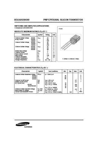
BC636/638/640 PNP EPITAXIAL SILICON TRANSISTOR SWITCHING AND AMPLIFIER APPLICATIONS Complement to BC635/637/639 TO-92 ABSOLUTE MAXIMUM RATINGS (T =25 ) A Characteristic Symbol Rating Unit Collector Emitter Voltage BC636 VCER -45 V at RBE=1Kohm BC638 -60 V BC640 -100 V Collector Emitter Voltage BC636 VCES -45 V BC638 -60 V BC640 -100 V Collector Emitter Voltage BC636 VCE
0.24. Size:74K rohm
dtc643tu.pdf
DTC643TU / DTC643TK Transistors Digital transistors (built-in resistor) DTC643TU / DTC643TK External dimensions (Unit mm) Features In addition to the features of regular digital transistors. 2.0 0.2 UMT3 1) Low saturation voltage, typically 1.3 0.1 0.9 0.1 0.65 0.65 VCE (sat) =40mV at IC / IB=50mA / 2.5mA, makes these 0.2 0.7 0.1 (1) (2) transistors ideal
0.25. Size:191K onsemi
fdc645n.pdf

Is Now Part of To learn more about ON Semiconductor, please visit our website at www.onsemi.com Please note As part of the Fairchild Semiconductor integration, some of the Fairchild orderable part numbers will need to change in order to meet ON Semiconductor s system requirements. Since the ON Semiconductor product management systems do not have the ability to manage part nomenclatur
0.26. Size:1310K onsemi
fdc642p-f085 fdc642p-f085p.pdf
MOSFET P-Channel, POWERTRENCH -20 V, -4 A, 100 mW FDC642P-F085, FDC642P-F085P www.onsemi.com Features Typ RDS(on) = 52.5 mW at VGS = -4.5 V, ID = -4 A Typ RDS(on) = 75.3 mW at VGS = -2.5 V, ID = -3.2 A Fast Switching Speed Low Gate Charge (6.9 nC Typical) TSOT23 6-Lead High Performance Trench Technology for Extremely Low RDS(on) CASE 419BL SUPERSOTt-6 P
0.27. Size:228K onsemi
ntmfs5c646n.pdf
MOSFET Power, Single, N-Channel 60 V, 5.0 mW, 93 A NTMFS5C646N Features www.onsemi.com Small Footprint (5x6 mm) for Compact Design Low RDS(on) to Minimize Conduction Losses V(BR)DSS RDS(ON) MAX ID MAX Low QG and Capacitance to Minimize Driver Losses These Devices are Pb-Free, Halogen Free/BFR Free and are RoHS 60 V 5.0 mW @ 10 V 93 A Compliant MAXIMUM RATINGS (T
0.28. Size:190K onsemi
fdc6401n.pdf

Is Now Part of To learn more about ON Semiconductor, please visit our website at www.onsemi.com Please note As part of the Fairchild Semiconductor integration, some of the Fairchild orderable part numbers will need to change in order to meet ON Semiconductor s system requirements. Since the ON Semiconductor product management systems do not have the ability to manage part nomenclatur
0.29. Size:92K onsemi
bc640-016g.pdf
BC640-016G High Current Transistors PNP Silicon Features This is a Pb-Free Device http //onsemi.com COLLECTOR 2 MAXIMUM RATINGS 3 Rating Symbol Value Unit BASE Collector-Emitter Voltage VCEO -80 Vdc Collector-Base Voltage VCBO -80 Vdc 1 Emitter-Base Voltage VEBO -5.0 Vdc EMITTER Collector Current - Continuous IC -0.5 Adc Total Device Dissipation @ TA = 25 C PD 625 mW Derat
0.30. Size:226K onsemi
nvd5c648nl.pdf
NVD5C648NL MOSFET Power, Single N-Channel 60 V, 4.1 mW, 89 A Features www.onsemi.com Low RDS(on) to Minimize Conduction Losses Low QG and Capacitance to Minimize Driver Losses V(BR)DSS RDS(on) ID AEC-Q101 Qualified and PPAP Capable 4.1 mW @ 10 V These Devices are Pb-Free, Halogen Free/BFR Free and are RoHS 60 V 89 A Compliant 5.7 mW @ 4.5 V MAXIMUM RATINGS (TJ
0.31. Size:114K onsemi
ntmfs5c645nl.pdf
NTMFS5C645NL Power MOSFET 60 V, 4.0 mW, 100 A, Single N-Channel Features Small Footprint (5x6 mm) for Compact Design Low RDS(on) to Minimize Conduction Losses www.onsemi.com Low QG and Capacitance to Minimize Driver Losses These Devices are Pb-Free and are RoHS Compliant V(BR)DSS RDS(ON) MAX ID MAX MAXIMUM RATINGS (TJ = 25 C unless otherwise noted) 4.0 mW @ 10 V 60
0.33. Size:113K onsemi
ntmfs5c646nl.pdf
NTMFS5C646NL Power MOSFET 60 V, 4.7 mW, 93 A, Single N-Channel Features Small Footprint (5x6 mm) for Compact Design Low RDS(on) to Minimize Conduction Losses www.onsemi.com Low QG and Capacitance to Minimize Driver Losses These Devices are Pb-Free and are RoHS Compliant V(BR)DSS RDS(ON) MAX ID MAX MAXIMUM RATINGS (TJ = 25 C unless otherwise noted) 4.7 mW @ 10 V 60 V
0.34. Size:179K onsemi
nvmfs5c645nl.pdf
NVMFS5C645NL Power MOSFET 60 V, 4.0 mW, 100 A, Single N-Channel Features Small Footprint (5x6 mm) for Compact Design Low RDS(on) to Minimize Conduction Losses www.onsemi.com Low QG and Capacitance to Minimize Driver Losses NVMFS5C645NLWF - Wettable Flank Option for Enhanced Optical Inspection V(BR)DSS RDS(ON) MAX ID MAX AEC-Q101 Qualified and PPAP Capable 4.0 mW
0.35. Size:74K onsemi
nvmfs5c646nl.pdf
NVMFS5C646NL Power MOSFET 60 V, 4.7 mW, 93 A, Single N-Channel Features Small Footprint (5x6 mm) for Compact Design Low RDS(on) to Minimize Conduction Losses www.onsemi.com Low QG and Capacitance to Minimize Driver Losses NVMFS5C646NLWF - Wettable Flank Option for Enhanced Optical Inspection V(BR)DSS RDS(ON) MAX ID MAX AEC-Q101 Qualified and PPAP Capable 4.7 mW @
0.36. Size:289K onsemi
bc640ta.pdf

Is Now Part of To learn more about ON Semiconductor, please visit our website at www.onsemi.com Please note As part of the Fairchild Semiconductor integration, some of the Fairchild orderable part numbers will need to change in order to meet ON Semiconductor s system requirements. Since the ON Semiconductor product management systems do not have the ability to manage part nomenclatur
0.39. Size:115K cdil
bc635 bc636 bc637 bc638 bc639 bc640.pdf
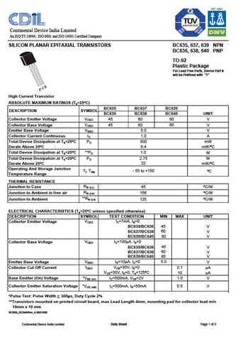
Continental Device India Limited An ISO/TS 16949, ISO 9001 and ISO 14001 Certified Company SILICON PLANAR EPITAXIAL TRANSISTORS BC635, 637, 639 NPN BC636, 638, 640 PNP TO-92 Plastic Package For Lead Free Parts, Device Part # will be Prefixed with "T" B C E High Current Transistor ABSOLUTE MAXIMUM RATINGS (Ta=25 C) BC635 BC637 BC639 DESCRIPTION SYMBOL BC636 BC638 BC640 UNIT VCE
0.40. Size:473K jiangsu
bc636 bc638 bc640.pdf
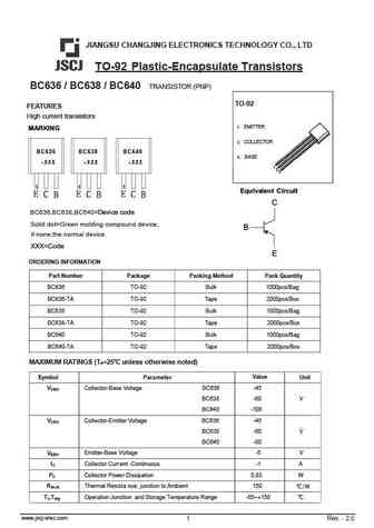
JIANGSU CHANGJING ELECTRONICS TECHNOLOGY CO., LTD TO-92 Plastic-Encapsulate Transistors BC636 / BC638 / BC640 TRANSISTOR (PNP) TO-92 FEATURES High current transistors 1. EMITTER 2. COLLECTOR BC636 BC638 BC640 3. BASE XXX XXX XXX 1 1 1 Equivalent Circuit BC636,BC638,BC640=Device code Solid dot=Green molding compound device, if none,the normal device XXX=Co
0.41. Size:144K jmnic
2sc643a.pdf
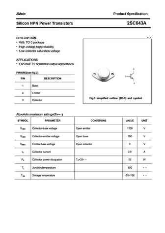
JMnic Product Specification Silicon NPN Power Transistors 2SC643A DESCRIPTION With TO-3 package High voltage,high reliability Low collector saturation voltage APPLICATIONS For color TV horizontal output applications PINNING(see fig.2) PIN DESCRIPTION 1 Base 2 Emitter Fig.1 simplified outline (TO-3) and symbol 3 Collector Absolute maximum ratings(Ta= ) SYMB
0.42. Size:144K jmnic
2sc643.pdf
JMnic Product Specification Silicon NPN Power Transistors 2SC643 DESCRIPTION With TO-3 package High voltage,high reliability Low collector saturation voltage APPLICATIONS For color TV horizontal output applications PINNING(see fig.2) PIN DESCRIPTION 1 Base 2 Emitter Fig.1 simplified outline (TO-3) and symbol 3 Collector Absolute maximum ratings(Ta= ) SYMBO
0.43. Size:68K kec
krc641t-krc646t.pdf
SEMICONDUCTOR KRC641T KRC646T TECHNICAL DATA EPITAXIAL PLANAR NPN TRANSISTOR HIGH CURRENT SWITCHING APPLICATION. INTERFACE CIRCUIT AND DRIVER CIRCUIT APPPLICATION. E B FEATURES DIM MILLIMETERS _ A 2.9 + 0.2 15 With Built-in Bias Resistors. B 1.6+0.2/-0.1 _ C 0.70 + 0.05 Simplify Circuit Design. 2 _ D 0.4 + 0.1 Reduce a Quantity of Parts and Manufacturing Process. E 2.8+
0.44. Size:226K lge
bc636 bc638 bc640.pdf
BC636/BC638/BC640 Transistor(PNP) 1. EMITTER TO-92 2. COLLECTOR 3. BASE Features High current transistors MAXIMUM RATINGS (TA=25 unless otherwise noted) Symbol Parameter Value Units VCBO Collector-Base Voltage BC636 -45 BC638 -60 V BC640 -100 VCEO Collector-Emitter Voltage BC636 -45 BC638 -60 V BC640 -80 Dimensions in inches and (millimeters) VEBO Emitter-
0.45. Size:691K kexin
dtc643tk.pdf
SMD Type Transistors Digital Transistors DTC643TK (KDTC643TK) SOT-23 Unit mm +0.1 2.9 -0.1 +0.1 0.4-0.1 3 Features Collector Current Capability IC=600mA Collector Emitter Voltage VCEO=20V 1 2 +0.1 +0.05 0.95 -0.1 0.1 -0.01 +0.1 1.9 -0.1 1.Base C 2.Emitter B 3.collector R E R=4.7k Absolute Maximum Ratings Ta = 25 Parameter Symbol Rating Unit
0.46. Size:1570K kexin
fdc642p.pdf
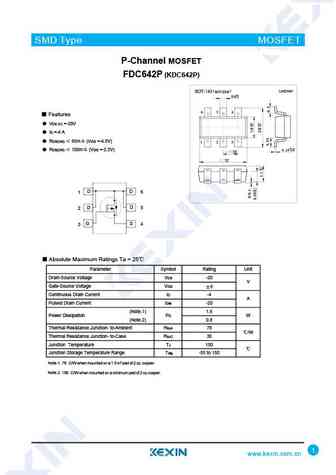
SMD Type MOSFET P-Channel MOSFET FDC642P (KDC642P) ( ) SOT-23-6 Unit mm +0.1 0.4 -0.1 6 5 4 Features VDS (V) =-20V ID =-4 A RDS(ON) 65m (VGS =-4.5V) 2 3 1 +0.02 RDS(ON) 100m (VGS =-2.5V) 0.15 -0.02 +0.01 -0.01 +0.2 -0.1 D D 6 1 D D 5 2 G S 4 3 Absolute Maximum Ratings Ta = 25 Parameter Symbol Rating Unit Drain-Source Vol
0.47. Size:82K chenmko
chdtc643tugp.pdf
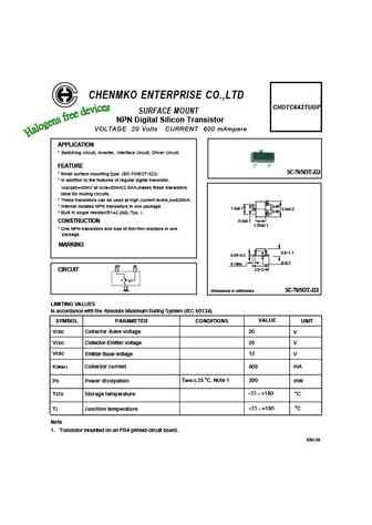
CHENMKO ENTERPRISE CO.,LTD CHDTC643TUGP SURFACE MOUNT NPN Digital Silicon Transistor VOLTAGE 20 Volts CURRENT 600 mAmpere APPLICATION * Switching circuit, Inverter, Interface circuit, Driver circuit. FEATURE SC-70/SOT-323 * Small surface mounting type. (SC-70/SOT-323) * In addition to the features of regular digital transistor. VCE(sat)=40mV at IC/IB=50mA/2.5mA,makes these transist
0.48. Size:77K chenmko
chdtc643tkgp.pdf
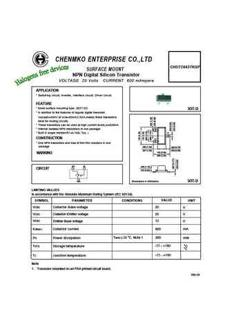
CHENMKO ENTERPRISE CO.,LTD CHDTC643TKGP SURFACE MOUNT NPN Digital Silicon Transistor VOLTAGE 20 Volts CURRENT 600 mAmpere APPLICATION * Switching circuit, Inverter, Interface circuit, Driver circuit. FEATURE * Small surface mounting type. (SOT-23) SOT-23 * In addition to the features of regular digital transistor. VCE(sat)=40mV at IC/IB=50mA/2.5mA,makes these transistors ideal fo
0.49. Size:1544K cn vbsemi
fdc6420c.pdf
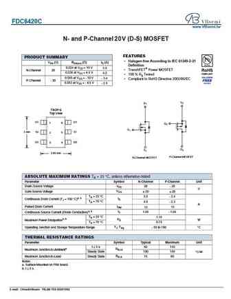
FDC6420C www.VBsemi.tw N- and P-Channel 2 V (D-S) MOSFET 0 FEATURES PRODUCT SUMMARY Halogen-free According to IEC 61249-2-21 VDS (V) RDS(on) ( )ID (A) Definition 0.024 at VGS = 10 V 5.5 TrenchFET Power MOSFET N-Channel 20 0.036 at VGS = 4.5 V 4.2 100 % Rg Tested 0.069 at VGS = - 10 V - 3.4 Compliant to RoHS Directive 2002/95/EC P-Channel - 20 0.083 at V
0.50. Size:115K inchange semiconductor
2sc643a.pdf
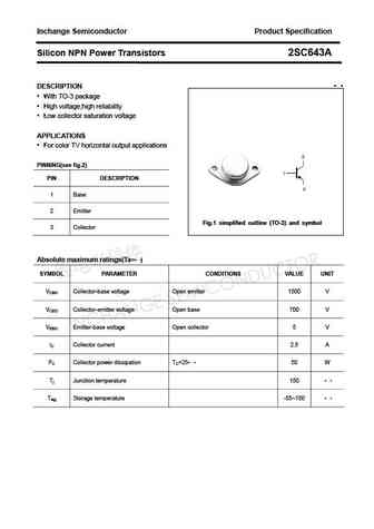
Inchange Semiconductor Product Specification Silicon NPN Power Transistors 2SC643A DESCRIPTION With TO-3 package High voltage,high reliability Low collector saturation voltage APPLICATIONS For color TV horizontal output applications PINNING(see fig.2) PIN DESCRIPTION 1 Base 2 Emitter Fig.1 simplified outline (TO-3) and symbol 3 Collector Absolute maximum ratin
0.51. Size:265K inchange semiconductor
nvd5c648nl.pdf
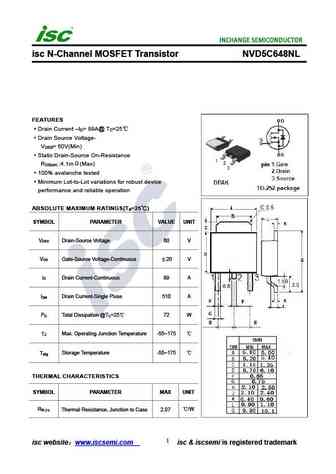
isc N-Channel MOSFET Transistor NVD5C648NL FEATURES Drain Current I = 89A@ T =25 D C Drain Source Voltage- V = 60V(Min) DSS Static Drain-Source On-Resistance R 4.1m (Max) DS(on) 100% avalanche tested Minimum Lot-to-Lot variations for robust device performance and reliable operation ABSOLUTE MAXIMUM RATINGS(T =25 ) a SYMBOL PARAMETER VALUE UNIT V Drain-Source
0.52. Size:177K inchange semiconductor
2sc643.pdf
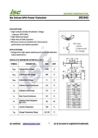
INCHANGE Semiconductor isc Silicon NPN Power Transistor 2SC643 DESCRIPTION High Collector-Emitter Breakdown Voltage- V = 800V (Min) (BR)CEO High Switching Speed Wide Area of Safe Operation Minimum Lot-to-Lot variations for robust device performance and reliable operation APPLICATIONS Designed for high speed switching and horizontal deflection output applications. ABSOLU
Otros transistores... C5T5401
, C5T5550
, C5T5551
, C5T6539
, C5T6540
, C5T918
, C6
, C63
, A733
, C651
, C652
, C7
, C7076
, C720
, C722
, C740
, C742
.
History: 2SC2539
| 2SD1053
| 2SD1054
| 2SD1052A