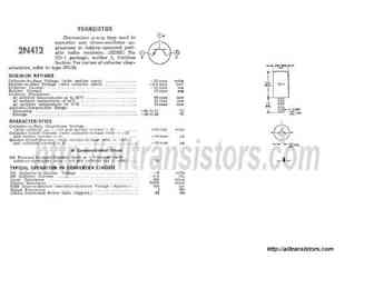
2N41 Equivalente. Reemplazo. Hoja de especificaciones. Principales características
Número de Parte: 2N41
Material: Ge
Polaridad de transistor: PNP
ESPECIFICACIONES MÁXIMAS
Disipación total del dispositivo (Pc): 0.05 W
Tensión colector-base (Vcb): 25 V
Corriente del colector DC máxima (Ic): 0.015 A
Temperatura operativa máxima (Tj): 50 °C
CARACTERÍSTICAS ELÉCTRICAS
Transición de frecuencia (fT): 0.2 MHz
Ganancia de corriente contínua (hFE): 40
Encapsulados: TO1
Búsqueda de reemplazo de 2N41
- Selecciónⓘ de transistores por parámetros
2N41 datasheet
2n4125 2n4126.pdf
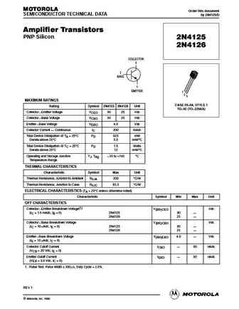
MOTOROLA Order this document SEMICONDUCTOR TECHNICAL DATA by 2N4125/D Amplifier Transistors PNP Silicon 2N4125 2N4126 COLLECTOR 3 2 BASE 1 EMITTER 1 2 3 MAXIMUM RATINGS CASE 29 04, STYLE 1 Rating Symbol 2N4125 2N4126 Unit TO 92 (TO 226AA) Collector Emitter Voltage VCEO 30 25 Vdc Collector Base Voltage VCBO 30 25 Vdc Emitter Base Voltage VEBO 4.0 Vdc Collector
2n4123 2n4124.pdf
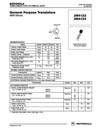
MOTOROLA Order this document SEMICONDUCTOR TECHNICAL DATA by 2N4123/D General Purpose Transistors NPN Silicon 2N4123 2N4124 COLLECTOR 3 2 BASE 1 EMITTER 1 2 3 MAXIMUM RATINGS CASE 29 04, STYLE 1 Rating Symbol 2N4123 2N4124 Unit TO 92 (TO 226AA) Collector Emitter Voltage VCEO 30 25 Vdc Collector Base Voltage VCBO 40 30 Vdc Emitter Base Voltage VEBO 5.0 Vdc Col
2n4126 cnv 2.pdf
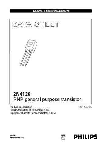
DISCRETE SEMICONDUCTORS DATA SHEET book, halfpage M3D186 2N4126 PNP general purpose transistor 1997 Mar 25 Product specification Supersedes data of September 1994 File under Discrete Semiconductors, SC04 Philips Semiconductors Product specification PNP general purpose transistor 2N4126 FEATURES PINNING Low current (max. 200 mA) PIN DESCRIPTION Low voltage (max. 25 V). 1
2n4124 cnv 2.pdf

DISCRETE SEMICONDUCTORS DATA SHEET book, halfpage M3D186 2N4124 NPN general purpose transistor 1997 Mar 25 Product specification Supersedes data of September 1994 File under Discrete Semiconductors, SC04 Philips Semiconductors Product specification NPN general purpose transistor 2N4124 FEATURES PINNING Low current (max. 200 mA) PIN DESCRIPTION Low voltage (max. 25 V). 1
2n4125.pdf
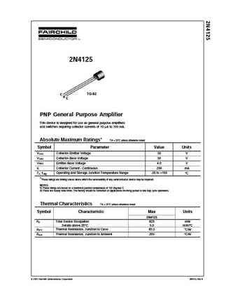
2N4125 C TO-92 B E PNP General Purpose Amplifier This device is designed for use as general purpose amplifiers and switches requiring collector currents of 10 A to 100 mA. Absolute Maximum Ratings* TA = 25 C unless otherwise noted Symbol Parameter Value Units V Collector-Emitter Voltage 30 V CEO V Collector-Base Voltage 30 V CBO V Emitter-Base Voltage 4.0 V EBO I Collector Cur
2n4124 mmbt4124.pdf
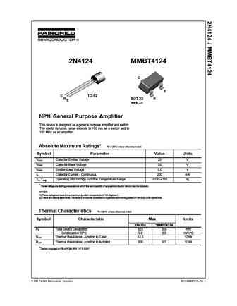
2N4124 MMBT4124 C E TO-92 C B B SOT-23 E Mark ZC NPN General Purpose Amplifier This device is designed as a general purpose amplifier and switch. The useful dynamic range extends to 100 mA as a switch and to 100 MHz as an amplifier. Absolute Maximum Ratings* TA = 25 C unless otherwise noted Symbol Parameter Value Units VCEO Collector-Emitter Voltage 25 V VCBO Collector-Base Vo
2n4123.pdf

[]]]]]]]]]]]]]]] []]]]]]]]]]]]]] 2N4123 C TO-92 B E NPN General Purpose Amplifier This device is designed for use as general purpose amplifiers and switches requiring collector currents to 100 mA. Absolute Maximum Ratings* TA = 25 C unless otherwise noted Symbol Parameter Value Units VCEO Collector-Emitter Voltage 30 V V Collector-Base Voltage 40 V CBO VEBO Emitter-Base Voltage
2n4126 mmbt4126.pdf
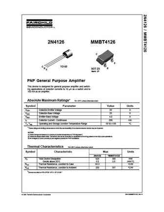
2N4126 MMBT4126 C E C TO-92 B B SOT-23 E Mark ZF PNP General Purpose Amplifier This device is designed for general purpose amplifier and switch- ing applications at collector currents to 10 A as a switch and to 100 mA as an amplifier. Absolute Maximum Ratings* TA = 25 C unless otherwise noted Symbol Parameter Value Units VCEO Collector-Emitter Voltage 25 V VCBO Collector-Base
2n4117a pn4117a sst4117 2n4118a pn4118a sst4118 2n4119a pn4119a sst4119.pdf
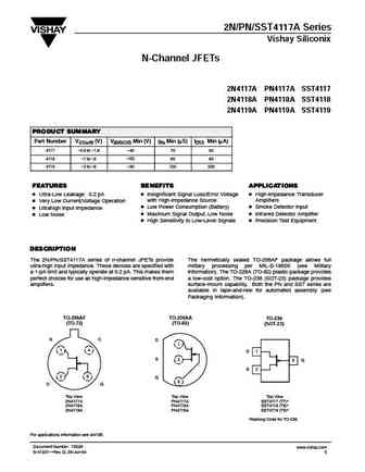
2N/PN/SST4117A Series Vishay Siliconix N-Channel JFETs 2N4117A PN4117A SST4117 2N4118A PN4118A SST4118 2N4119A PN4119A SST4119 PRODUCT SUMMARY Part Number VGS(off) (V) V(BR)GSS Min (V) gfs Min (mS) IDSS Min (mA) 4117 -0.6 to -1.8 -40 70 30 4118 -1 to -3 -40 80 80 4119 -2 to -6 -40 100 200 FEATURES BENEFITS APPLICATIONS D Ultra-Low Leakage 0.2 pA D Insignificant Signal Loss/Error Vo
2n4123 2n4124 2n4125 2n4126.pdf
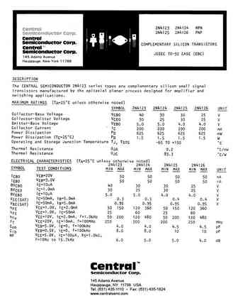
TM Central Semiconductor Corp. 145 Adams Avenue Hauppauge, NY 11788 USA Tel (631) 435-1110 Fax (631) 435-1824 www.centralsemi.com
2n4124g.pdf

2N4123, 2N4124 General Purpose Transistors NPN Silicon http //onsemi.com Features Pb-Free Packages are Available* COLLECTOR 3 MAXIMUM RATINGS 2 Rating Symbol Value Unit BASE Collector-Emitter Voltage VCEO Vdc 2N4123 30 2N4124 25 1 EMITTER Collector-Base Voltage VCBO Vdc 2N4123 40 2N4124 30 Emitter-Base Voltage VEBO 5.0 Vdc Collector Current - Continuous IC 200 mAdc TO
2n4123 2n4124.pdf
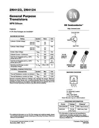
2N4123, 2N4124 General Purpose Transistors NPN Silicon http //onsemi.com Features Pb-Free Packages are Available* COLLECTOR 3 MAXIMUM RATINGS 2 Rating Symbol Value Unit BASE Collector-Emitter Voltage VCEO Vdc 2N4123 30 2N4124 25 1 EMITTER Collector-Base Voltage VCBO Vdc 2N4123 40 2N4124 30 Emitter-Base Voltage VEBO 5.0 Vdc Collector Current - Continuous IC 200 mAdc TO
2n4114.pdf
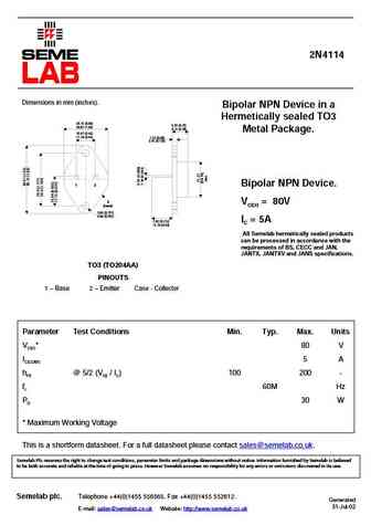
2N4114 Dimensions in mm (inches). Bipolar NPN Device in a Hermetically sealed TO3 25.15 (0.99) 6.35 (0.25) 26.67 (1.05) 9.15 (0.36) Metal Package. 10.67 (0.42) 11.18 (0.44) 1.52 (0.06) 3.43 (0.135) 1 2 Bipolar NPN Device. 3 VCEO = 80V (case) 3.84 (0.151) 4.09 (0.161) 7.92 (0.312) IC = 5A 12.70 (0.50) All Semelab hermetically sealed products can be processed in ac
2n4113.pdf
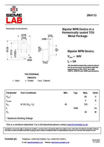
2N4113 Dimensions in mm (inches). Bipolar NPN Device in a Hermetically sealed TO3 25.15 (0.99) 6.35 (0.25) 26.67 (1.05) 9.15 (0.36) Metal Package. 10.67 (0.42) 11.18 (0.44) 1.52 (0.06) 3.43 (0.135) 1 2 Bipolar NPN Device. 3 VCEO = 80V (case) 3.84 (0.151) 4.09 (0.161) 7.92 (0.312) IC = 5A 12.70 (0.50) All Semelab hermetically sealed products can be processed in ac
2n4104.pdf
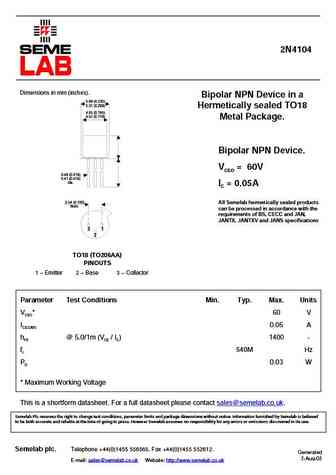
2N4104 Dimensions in mm (inches). Bipolar NPN Device in a 5.84 (0.230) 5.31 (0.209) Hermetically sealed TO18 4.95 (0.195) 4.52 (0.178) Metal Package. Bipolar NPN Device. VCEO = 60V 0.48 (0.019) 0.41 (0.016) dia. IC = 0.05A 2.54 (0.100) All Semelab hermetically sealed products Nom. can be processed in accordance with the requirements of BS, CECC and JAN, JANTX, JA
2n4124.pdf
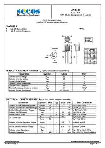
2N4124 0.2 A, 30 V NPN Plastic Encapsulated Transistor Elektronische Bauelemente RoHS Compliant Product A suffix of -C specifies halogen & lead-free FEATURES TO-92 High DC Current Gain High Transition Frequency G H Emitter Base Collector J A D B Collector Millimeter REF. Min. Max. K A 4.40 4.70 B 4.30 4.70 C 12.70 - D 3.30 3.
2n4126.pdf
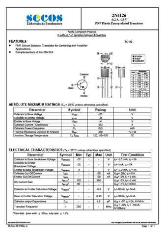
2N4126 -0.2 A, -25 V PNP Plastic Encapsulated Transistor Elektronische Bauelemente RoHS Compliant Product A suffix of -C specifies halogen & lead-free FEATURES TO-92 PNP Silicon Epitaxial Transistor for Switching and Amplifier Applications. Complementary of the 2N4124 G H Emitter Base Collector J A D Millimeter REF. B Min. Max. Collecto
2n4117 2n4118 2n4119 pn4117 pn4118 pn4119 sst4117 sst4118 sst4119.pdf
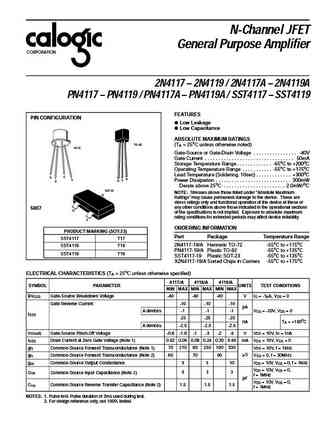
N-Channel JFET General Purpose Amplifier CORPORATION 2N4117 2N4119 / 2N4117A 2N4119A PN4117 PN4119 / PN4117A PN4119A / SST4117 SST4119 FEATURES PIN CONFIGURATION Low Leakage Low Capacitance ABSOLUTE MAXIMUM RATINGS TO-92 (T = 25oC unless otherwise noted) A TO-72 Gate-Source or Gate-Drain Voltage . . . . . . . . . . . . . . . . -40V Gate Curre
2n4150u3.pdf

TECHNICAL DATA SHEET 6 Lake Street, Lawrence, MA 01841 1-800-446-1158 / (978) 620-2600 / Fax (978) 689-0803 Website http //www.microsemi.com NPN POWER SILICON TRANSISTOR Qualified per MIL-PRF-19500/394 DEVICES LEVELS JAN 2N4150 2N5237 2N5238 JANTX 2N4150S 2N5237S 2N5238S JANTXV JANS ABSOLUTE MAXIMUM RATINGS (TC = +25 C unless otherwise noted) 2N4150 2N5237 2N5238
2n4150s.pdf
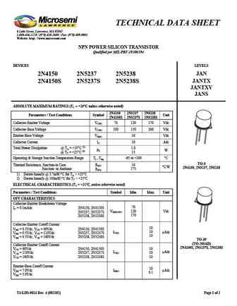
TECHNICAL DATA SHEET 6 Lake Street, Lawrence, MA 01841 1-800-446-1158 / (978) 620-2600 / Fax (978) 689-0803 Website http //www.microsemi.com NPN POWER SILICON TRANSISTOR Qualified per MIL-PRF-19500/394 DEVICES LEVELS JAN 2N4150 2N5237 2N5238 JANTX 2N4150S 2N5237S 2N5238S JANTXV JANS ABSOLUTE MAXIMUM RATINGS (TC = +25 C unless otherwise noted) 2N4150 2N5237 2N5238
wpt2n41.pdf
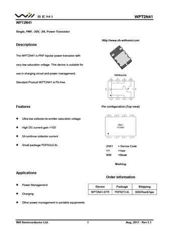
WPT2N41 WPT2N41 Single, PNP, -30V, -3A, Power Transistor Http //www.sh-willsemi.com Descriptions The WPT2N41 is PNP bipolar power transistor with very low saturation voltage. This device is suitable for use in charging circuit and power management. Standard Product WPT2N41 is Pb-free. Pin configuration (Top view) Features Ultra low collector-to-emitter saturation volta
2n4150 2n5237 2n5238.pdf
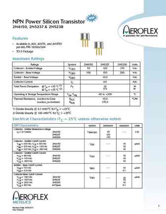
NPN Power Silicon Transistor 2N4150, 2N5237 & 2N5238 Features Available in JAN, JANTX, and JANTXV per MIL-PRF-19500/384 TO-5 Package Maximum Ratings Ratings Symbol 2N4150 2N5237 2N5238 Units Collector - Emitter Voltage VCEO 70 120 170 Vdc Collector - Base Voltage VCBO 100 150 200 Vdc Emitter - Base Voltage VEBO 10.0 Vdc Collector Current IC 4.0 Adc Total Power Dissipation @
2n3906 2n3973 2n3974 2n3975 2n3976 2n4058 2n4059 2n4060 2n4061 2n4062 2n4123 2n4124 2n4125 2n4126 2n4256 2n4264.pdf
2n4112.pdf

isc Silicon NPN Power Transistor 2N4112 DESCRIPTION Excellent Safe Operating Area Low Collector-Emitter Saturation Voltage 100% avalanche tested Minimum Lot-to-Lot variations for robust device performance and reliable operation. APPLICATIONS Designed for general-purpose switching and amplifier applications ABSOLUTE MAXIMUM RATINGS(T =25 ) a SYMBOL PARAMETER VALUE UNIT V
2n4114.pdf

isc Silicon NPN Power Transistor 2N4114 DESCRIPTION Excellent Safe Operating Area Low Collector-Emitter Saturation Voltage 100% avalanche tested Minimum Lot-to-Lot variations for robust device performance and reliable operation. APPLICATIONS Designed for general-purpose switching and amplifier applications ABSOLUTE MAXIMUM RATINGS(T =25 ) a SYMBOL PARAMETER VALUE UNIT V
2n4113.pdf

isc Silicon NPN Power Transistor 2N4113 DESCRIPTION Excellent Safe Operating Area Low Collector-Emitter Saturation Voltage 100% avalanche tested Minimum Lot-to-Lot variations for robust device performance and reliable operation. APPLICATIONS Designed for general-purpose switching and amplifier applications ABSOLUTE MAXIMUM RATINGS(T =25 ) a SYMBOL PARAMETER VALUE UNIT V
2n4111.pdf
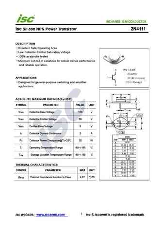
isc Silicon NPN Power Transistor 2N4111 DESCRIPTION Excellent Safe Operating Area Low Collector-Emitter Saturation Voltage 100% avalanche tested Minimum Lot-to-Lot variations for robust device performance and reliable operation. APPLICATIONS Designed for general-purpose switching and amplifier applications ABSOLUTE MAXIMUM RATINGS(T =25 ) a SYMBOL PARAMETER VALUE UNIT V
Otros transistores... 2N408 , 2N4080 , 2N4081 , 2N4086 , 2N4087 , 2N4087A , 2N409 , 2N4099 , BC557 , 2N410 , 2N4100 , 2N4104 , 2N4105 , 2N4106 , 2N4106A , 2N411 , 2N4111 .
🌐 : EN ES РУ

Liste
Recientemente añadidas las descripciónes de los transistores:
BJT: GA1A4M | SBT42 | 2SA200-Y | 2SA200-O | 2SD882-Q | 2SD882-P | 2SD882-E | 2SC945-L | 2SC945-H | 2SC4226-R23 | 2SC3357-F | 2SC3357-E | 2SC3356-R26 | 2SC3356-R24 | 2SC3356-R23 | 2SB772-Q | 2SB772-P | 2SB772-E | 2SA1015-L | 2SA1015-H | HSS8550
Popular searches
irfb4227 | irfb4110 | tip36c | bd139 transistor | irf840 datasheet | ge10001 | irf830 | irfp450