2N4395 Equivalente. Reemplazo. Hoja de especificaciones. Principales características
Número de Parte: 2N4395
Material: Si
Polaridad de transistor: NPN
ESPECIFICACIONES MÁXIMAS
Disipación total del dispositivo (Pc): 62
W
Tensión colector-base (Vcb): 60
V
Tensión colector-emisor (Vce): 40
V
Tensión emisor-base (Veb): 4
V
Corriente del colector DC máxima (Ic): 5
A
Temperatura operativa máxima (Tj): 200
°C
CARACTERÍSTICAS ELÉCTRICAS
Transición de frecuencia (ft): 4
MHz
Ganancia de corriente contínua (hfe): 50
Paquete / Cubierta:
TO3
Búsqueda de reemplazo de 2N4395
-
Selección ⓘ de transistores por parámetros
2N4395 datasheet
..1. Size:181K inchange semiconductor
2n4395.pdf 
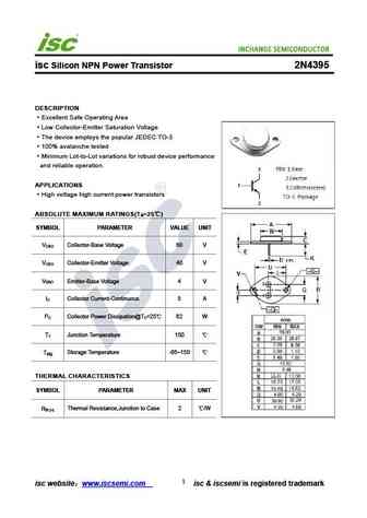
isc Silicon NPN Power Transistor 2N4395 DESCRIPTION Excellent Safe Operating Area Low Collector-Emitter Saturation Voltage The device employs the popular JEDEC TO-3 100% avalanche tested Minimum Lot-to-Lot variations for robust device performance and reliable operation. APPLICATIONS High voltage high current power transistors ABSOLUTE MAXIMUM RATINGS(T =25 ) a SYMBOL P
9.2. Size:59K vishay
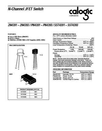
2n4391 pn4391 sst4391 2n4392 pn4392 sst4392 2n4393 pn4393 sst4393.pdf
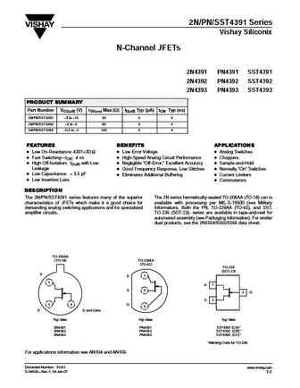
2N/PN/SST4391 Series Vishay Siliconix N-Channel JFETs 2N4391 PN4391 SST4391 2N4392 PN4392 SST4392 2N4393 PN4393 SST4393 PRODUCT SUMMARY Part Number VGS(off) (V) rDS(on) Max (W) ID(off) Typ (pA) tON Typ (ns) 2N/PN/SST4391 4 to 10 30 5 4 2N/PN/SST4392 2 to 5 60 5 4 2N/PN/SST4393 0.5 to 3 100 5 4 FEATURES BENEFITS APPLICATIONS D Low On-Resistance 4391
9.3. Size:106K central
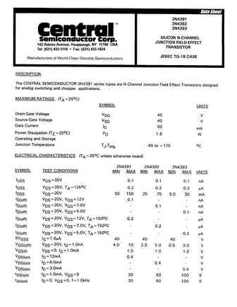
2n4391 2n4392 2n4393.pdf
145 Adams Avenue, Hauppauge, NY 11788 USA Tel (631) 435-1110 Fax (631) 435-1824 TM Central Semiconductor Corp. 145 Adams Avenue Hauppauge, NY 11788 USA Tel (631) 435-1110 Fax (631) 435-1824 www.centralsemi.com
9.5. Size:49K semelab
2n4393dcsm.pdf
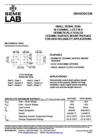
2N4393DCSM SEME LAB SMALL SIGNAL DUAL N CHANNEL J FET IN A HERMETICALLY SEALED CERAMIC SURFACE MOUNT PACKAGE FOR HIGH RELIABILITY APPLICATIONS MECHANICAL DATA Dimensions in mm (inches) 1.40 0.15 2.29 0.20 1.65 0.13 (0.055 0.006) (0.09 0.008) (0.065 0.005) FEATURES 2 3 HERMETIC CERAMIC SURFACE MOUNT 1 4 A PACKAGE 0.23 6 5 rad. (0.009) CECC SC
9.6. Size:15K semelab
2n4392.pdf
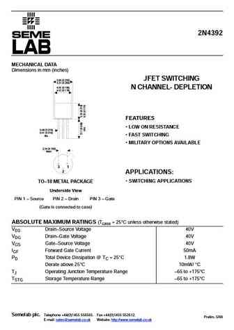
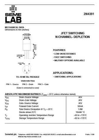
2N4392 MECHANICAL DATA Dimensions in mm (inches) JFET SWITCHING 5.84 (0.230) 5.31 (0.209) 4.95 (0.195) N CHANNEL- DEPLETION 4.52 (0.178) FEATURES LOW ON RESISTANCE 0.48 (0.019) 0.41 (0.016) FAST SWITCHING dia. MILITARY OPTIONS AVAILABLE 2.54 (0.100) Nom. 3 1 2 APPLICATIONS SWITCHING APPLICATIONS TO 18 METAL PACKAGE Underside View PIN 1 Source PIN 2
9.7. Size:13K semelab
2n4391.pdf
2N4391 MECHANICAL DATA Dimensions in mm (inches) JFET SWITCHING 5.84 (0.230) 5.31 (0.209) 4.95 (0.195) N CHANNEL- DEPLETION 4.52 (0.178) FEATURES LOW ON RESISTANCE 0.48 (0.019) 0.41 (0.016) FAST SWITCHING dia. MILITARY OPTIONS AVAILABLE 2.54 (0.100) Nom. 3 1 2 APPLICATIONS SWITCHING APPLICATIONS TO 18 METAL PACKAGE Underside View PIN 1 Source PIN 2
9.8. Size:229K semelab
2n4393c1a 2n4393c1b 2n4393c1c 2n4393c1d.pdf
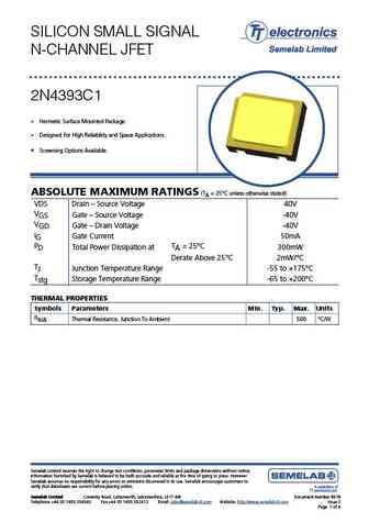
SILICON SMALL SIGNAL N-CHANNEL JFET 2N4393C1 Hermetic Surface Mounted Package. Designed For High Reliability and Space Applications. Screening Options Available. ABSOLUTE MAXIMUM RATINGS (TA = 25 C unless otherwise stated) VDS Drain Source Voltage 40V VGS Gate Source Voltage -40V VGD Gate Drain Voltage -40V IG Gate Current 50mA PD TA = 25 C
9.10. Size:38K inchange semiconductor
2n4399.pdf

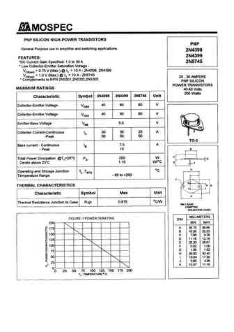
INCHANGE Semiconductor isc Product Specification isc Silicon PNP Power Transistors 2N4399 DESCRIPTION Low Collector Saturation Voltage- VCE(sat)= -1.0V(Max.)@ IC= -15A Wide Area of Safe Operation Complement to Type 2N5302 APPLICATIONS Designed for use in power amplifier and switching circuits. ABSOLUTE MAXIMUM RATINGS(Ta=25 ) SYMBOL PARAMETER VALUE UNIT V Coll
9.11. Size:38K inchange semiconductor
2n4398.pdf
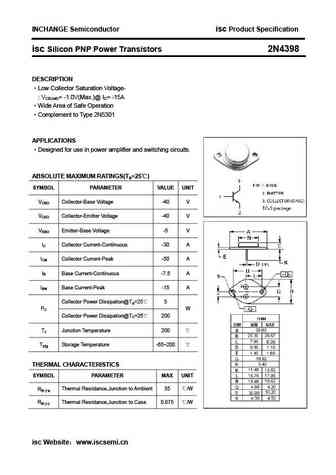
INCHANGE Semiconductor isc Product Specification isc Silicon PNP Power Transistors 2N4398 DESCRIPTION Low Collector Saturation Voltage- VCE(sat)= -1.0V(Max.)@ IC= -15A Wide Area of Safe Operation Complement to Type 2N5301 APPLICATIONS Designed for use in power amplifier and switching circuits. ABSOLUTE MAXIMUM RATINGS(Ta=25 ) SYMBOL PARAMETER VALUE UNIT V Coll
9.12. Size:182K inchange semiconductor
2n4396.pdf
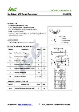
isc Silicon NPN Power Transistor 2N4396 DESCRIPTION Excellent Safe Operating Area Low Collector-Emitter Saturation Voltage The device employs the popular JEDEC TO-3 100% avalanche tested Minimum Lot-to-Lot variations for robust device performance and reliable operation. APPLICATIONS High voltage high current power transistors ABSOLUTE MAXIMUM RATINGS(T =25 ) a SYMBOL P
9.13. Size:121K inchange semiconductor
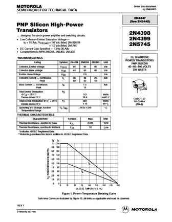
2n4398 2n4399 2n5745.pdf
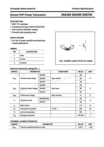
Inchange Semiconductor Product Specification Silicon PNP Power Transistors 2N4398 2N4399 2N5745 DESCRIPTION With TO-3 package Complement to type 2N5301/5302/5303 Low collector saturation voltage Excellent safe operating area APPLICATIONS For use in power amplifier and switching circuits applications. PINNING PIN DESCRIPTION 1 Base 2 Emitter Fig.1 simplified o
Otros transistores... 2N4385
, 2N4386
, 2N4387
, 2N4388
, 2N4389
, 2N438A
, 2N439
, 2N4390
, S8050
, 2N4396
, 2N4397
, 2N4398
, 2N4399
, 2N439A
, 2N43A
, 2N44
, 2N440
.