P302 Datasheet. Equivalente. Reemplazo. Hoja de especificaciones. Principales características
Número de Parte: P302 📄📄
Material: Si
Polaridad de transistor: PNP
ESPECIFICACIONES MÁXIMAS
Disipación total del dispositivo (Pc): 7 W
Tensión colector-base (Vcb): 35 V
Corriente del colector DC máxima (Ic): 0.5 A
Temperatura operativa máxima (Tj): 150 °C
CARACTERÍSTICAS ELÉCTRICAS
Transición de frecuencia (fT): 0.2 MHz
Ganancia de corriente contínua (hFE): 10
Búsqueda de reemplazo de P302
- Selecciónⓘ de transistores por parámetros
P302 datasheet
0.1. Size:50K motorola
tp3024br.pdf 
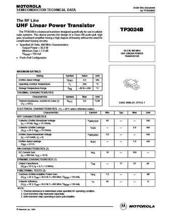
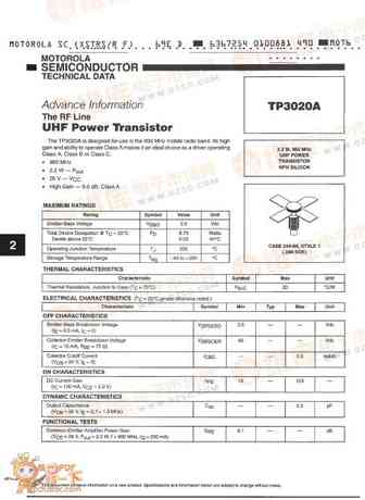
MOTOROLA Order this document SEMICONDUCTOR TECHNICAL DATA by TP3024B/D The RF Line UHF Linear Power Transistor TP3024B The TP3024B is a balanced transistor designed specifically for use in cellular radio systems. This device permits the design of a Class AB push pull, high gain, broadband amplifier having a high degree of linearity without the need for complicated biasing circuitry.
0.3. Size:93K motorola
tp3021re.pdf
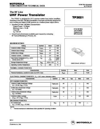
MOTOROLA Order this document SEMICONDUCTOR TECHNICAL DATA by TP3021/D The RF Line UHF Power Transistor TP3021 The TP3021 is designed for 24 V common emitter base station amplifiers. Operating in the 820 960 MHz bandwidth, it has been specifically designed for use in analog and digital (GSM) systems as a medium power output device. Specified 24 Volts, 960 MHz Characteristics Out
0.4. Size:51K motorola
tp3022br.pdf
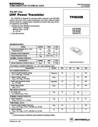
MOTOROLA Order this document SEMICONDUCTOR TECHNICAL DATA by TP3022B/D The RF Line UHF Power Transistor TP3022B The TP3022B is designed for common emitter operation in the 900 MHz mobile radio band. Use of gold metallization and silicon diffused ballast resistors results in a medium power output/driver transistor with state of the art ruggedness and reliability. Specifie
0.5. Size:280K st
stp3020l.pdf
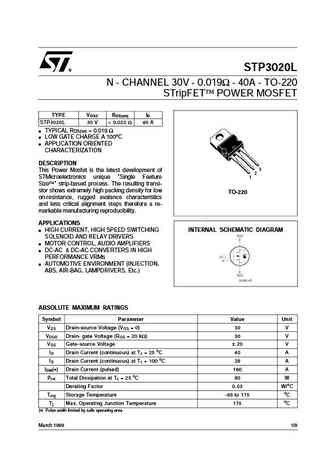
STP3020L N - CHANNEL 30V - 0.019 - 40A - TO-220 STripFET POWER MOSFET TYPE VDSS RDS(on) ID STP3020L 30 V
0.6. Size:123K sanyo
fp302.pdf
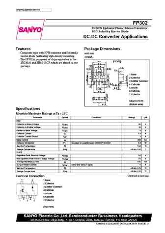
Ordering number EN4726 FP302 TR NPN Epitaxial Planar Silicon Transistor SBD Schottky Barrier Diode DC-DC Converter Applications Features Package Dimensions Composite type with NPN transistor and Schottoky unit mm barrier diode facilitating high-density mounting. 2099A The FP302 is composed of chips equivalent to the [FP302] 2SC4520 and SB05-05CP, which are placed in one pac
0.7. Size:462K sanyo
atp302.pdf
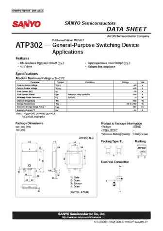
ATP302 Ordering number ENA1654A SANYO Semiconductors DATA SHEET P-Channel Silicon MOSFET General-Purpose Switching Device ATP302 Applications Features ON-resistance RDS(on)1=10m (typ.) Input capacitance Ciss=5400pF (typ.) 4.5V drive Halogen free compliance Specifications at Ta=25 C Absolute Maximum Ratings Parameter Symbol Conditions Ratings Unit Drai
0.8. Size:419K siemens
bup302.pdf
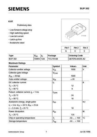
BUP 302 IGBT Preliminary data Low forward voltage drop High switching speed Low tail current Latch-up free Avalanche rated Pin 1 Pin 2 Pin 3 G C E Type VCE IC Package Ordering Code BUP 302 1000V 12A TO-218 AB Q67078-A4205-A2 Maximum Ratings Parameter Symbol Values Unit Collector-emitter voltage VCE 1000 V Collector-gate voltage VCGR RGE = 20 k 1000 Gate-
0.9. Size:26K siemens
byp302.pdf
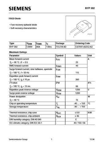
BYP 302 FRED Diode Fast recovery epitaxial diode Soft recovery characteristics Type VRRM IFRMS trr Package Ordering Code BYP 302 1200V 40A 130ns TO-218 AD C67047-A2252-A2 Maximum Ratings Parameter Symbol Values Unit Mean forward current IFAV A TC = 90 C, D = 0.5 25 RMS forward current IFRMS 40 Surge forward current, sine halfwave, aperiodic IFSM Tj = 100 C, f = 50 Hz 115
0.10. Size:416K diodes
dmp3028lk3.pdf
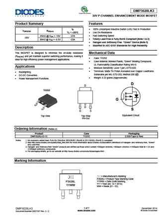
DMP3028LK3 30V P-CHANNEL ENHANCEMENT MODE MOSFET Product Summary Features ID 100% Unclamped Inductive Switch (UIS) Test In Production V(BR)DSS RDS(on) TC = +25 C Low On-Resistance Fast Switching Speed 25m @ VGS = -10V -27A -30V Totally Lead-Free & Fully RoHS Compliant (Note 1 & 2) 38m @ VGS = -4.5V -22A Halogen and Antimony Free. Green Devi
0.11. Size:404K diodes
dmp3028lfde.pdf
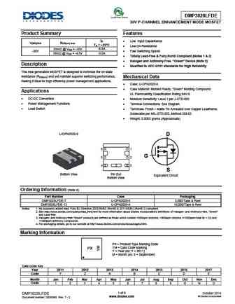
DMP3028LFDE 30V P-CHANNEL ENHANCEMENT MODE MOSFET Product Summary Features ID Low Input Capacitance V(BR)DSS RDS(on) max TA = +25 C Low On-Resistance 25m @ VGS = -10V -6.8A -30V Fast Switching Speed -5.0A 38m @ VGS = -4.5V Totally Lead-Free & Fully RoHS Compliant (Notes 1 & 2) Halogen and Antimony Free. Green Device (Note 3) Descripti
0.12. Size:197K diodes
dmp3020lss.pdf
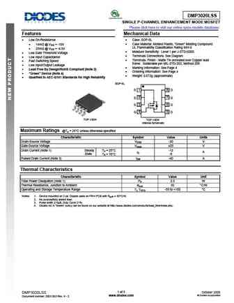
DMP3020LSS SINGLE P-CHANNEL ENHANCEMENT MODE MOSFET Please click here to visit our online spice models database. Features Mechanical Data Low On-Resistance Case SOP-8L 14m @ VGS = -10V Case Material Molded Plastic, Green Molding Compound. UL Flammability Classification Rating 94V-0 25m @ VGS = -4.5V Moisture Sensitivity Level 1 per J-STD-020D
0.13. Size:234K diodes
dmp3028lsd.pdf
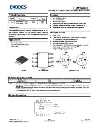
DMP3028LSD Maximum Ratings (@TA = +25 C, unless otherwise specified.) Characteristic Symbol Value Units Drain-Source Voltage VDSS -30 V Gate-Source Voltage 20 V VGSS Steady TA = +25 C -6 ID A State -4.7 TA = +70 C Continuous Drain Current (Note 5) VGS = 10V TA = +25 C -7.4 t
0.14. Size:355K onsemi
atp302.pdf
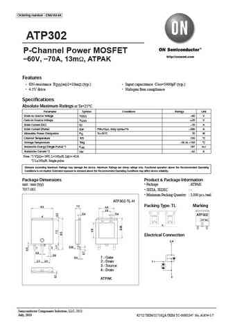
Ordering number ENA1654A ATP302 P-Channel Power MOSFET http //onsemi.com 60V, 70A, 13m , ATPAK Features ON-resistance RDS(on)1=10m (typ.) Input capacitance Ciss=5400pF (typ.) 4.5V drive Halogen free compliance Specifications Absolute Maximum Ratings at Ta=25 C Parameter Symbol Conditions Ratings Unit Drain-to-Source Voltage VDSS --60 V Gate-t
0.15. Size:32K russia
2p302a.pdf

p-n n-. 2302 P max, 300 U max,B 20 U max,B 20 U max,B 10 I max, 24 Tmax, C 125 U ,B 1...3.5 I,A 10 U,B 10 S,/ 5...12 U, 7 I , 3...24 11, 20 12, 8
0.18. Size:840K cn vbsemi
dmp3025lk3-13.pdf
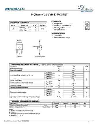
DMP3025LK3-13 www.VBsemi.tw P-Channel 30-V (D-S) MOSFET FEATURES PRODUCT SUMMARY Halogen-free VDS (V) RDS(on) ( ) ID (A)d Qg (Typ.) TrenchFET Power MOSFET 0.033 at VGS = - 10 V - 26 100 % Rg Tested RoHS - 30 19 nC COMPLIANT 100 % UIS Tested 0.046 at VGS = - 4.5 V - 21 APPLICATIONS Load Switch Notebook Adaptor Switch S TO-252 G G D S D Top View
0.19. Size:265K inchange semiconductor
dmp3028lk3.pdf
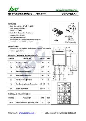
isc P-Channel MOSFET Transistor DMP3028LK3 FEATURES Drain Current I = -27A@ T =25 D C Drain Source Voltage- V = -30V(Min) DSS Static Drain-Source On-Resistance R = 25m (Max) DS(on) 100% avalanche tested Minimum Lot-to-Lot variations for robust device performance and reliable operation DESCRIPTION Designed for use in switch mode power supplies and general pu
Otros transistores... P217G, P217V, P27, P27A, P28, P29, P29A, P30, 431, P303, P303A, P304, P306, P306A, P307, P307A, P307B