SE2002 Equivalente. Reemplazo. Hoja de especificaciones. Principales características
Número de Parte: SE2002
Material: Si
Polaridad de transistor: NPN
ESPECIFICACIONES MÁXIMAS
Disipación total del dispositivo (Pc): 0.2 W
Tensión colector-base (Vcb): 35 V
Tensión colector-emisor (Vce): 20 V
Tensión emisor-base (Veb): 4 V
Corriente del colector DC máxima (Ic): 0.1 A
Temperatura operativa máxima (Tj): 125 °C
CARACTERÍSTICAS ELÉCTRICAS
Transición de frecuencia (fT): 200 MHz
Capacitancia de salida (Cc): 6 pF
Ganancia de corriente contínua (hFE): 100
Encapsulados: TO106
Búsqueda de reemplazo de SE2002
- Selecciónⓘ de transistores por parámetros
SE2002 datasheet
kse200.pdf
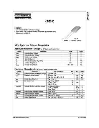
KSE200 Feature Low Collector-Emitter Saturation Voltage High Current Gain Bandwidth Product fT=65MHz @ IC=100mA (Min.) Complement to KSE210 TO-126 1 1. Emitter 2.Collector 3.Base NPN Epitaxial Silicon Transistor Absolute Maximum Ratings TC=25 C unless otherwise noted Symbol Parameter Value Units VCBO Collector-Base Voltage 40 V VCEO Collector-Emitter Voltage 25 V
kse200.pdf
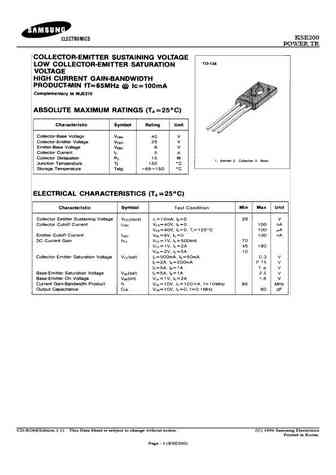
KSE200 POWER TR CD-ROM(Edition.1.1) This Data Sheet is subject to change without notice. (C) 1994 Samsung Electronics Printed in Korea. Page 1 (KSE200) KSE200 POWER TR CD-ROM(Edition.1.1) This Data Sheet is subject to change without notice. (C) 1994 Samsung Electronics Printed in Korea. Page 2 (KSE200)
se20075.pdf
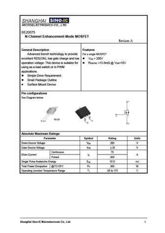
SE20075 N-Channel Enhancement-Mode MOSFET Revision A General Description Features For a single MOSFET Advanced trench technology to provide excellent RDS(ON), low gate charge and low V = 200V DS operation voltage. This device is suitable for R =15.8m @V =10V DS(ON) GS using as a load switch or in PWM applications. Simple Drive Requirement Small Package Outline
Otros transistores... SDT9308, SDT9309, SE0566, SE1001, SE1002, SE1022, SE1730, SE2001, TIP31, SE3001, SE3002, SE3005, SE4001, SE4002, SE4010, SE5006, SE5020
🌐 : EN ES РУ

Liste
Recientemente añadidas las descripciónes de los transistores:
BJT: GA1A4M | SBT42 | 2SA200-Y | 2SA200-O | 2SD882-Q | 2SD882-P | 2SD882-E | 2SC945-L | 2SC945-H | 2SC4226-R23 | 2SC3357-F | 2SC3357-E | 2SC3356-R26 | 2SC3356-R24 | 2SC3356-R23 | 2SB772-Q | 2SB772-P | 2SB772-E | 2SA1015-L | 2SA1015-H | HSS8550
Popular searches
2sc281 | m28s transistor | 2n3640 | tta1943 transistor | fb4410z | 2sa899 | 2sc1166 | jcs9n50fc datasheet