TK34 Datasheet. Equivalente. Reemplazo. Hoja de especificaciones. Principales características
Número de Parte: TK34 📄📄
Material: Ge
Polaridad de transistor: PNP
ESPECIFICACIONES MÁXIMAS
Disipación total del dispositivo (Pc): 0.1 W
Tensión colector-base (Vcb): 20 V
Tensión colector-emisor (Vce): 6 V
Tensión emisor-base (Veb): 15 V
Corriente del colector DC máxima (Ic): 0.05 A
Temperatura operativa máxima (Tj): 75 °C
CARACTERÍSTICAS ELÉCTRICAS
Transición de frecuencia (fT): 6 MHz
Ganancia de corriente contínua (hFE): 25
Encapsulados: X18
📄📄 Copiar
Búsqueda de reemplazo de TK34
- Selecciónⓘ de transistores por parámetros
TK34 datasheet
0.1. Size:255K toshiba
tk34e10n1.pdf 
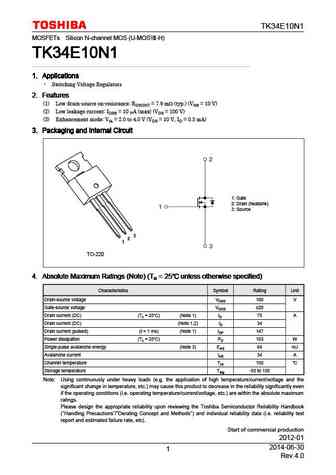
TK34E10N1 MOSFETs Silicon N-channel MOS (U-MOS -H) TK34E10N1 TK34E10N1 TK34E10N1 TK34E10N1 1. Applications 1. Applications 1. Applications 1. Applications Switching Voltage Regulators 2. Features 2. Features 2. Features 2. Features (1) Low drain-source on-resistance RDS(ON) = 7.9 m (typ.) (VGS = 10 V) (2) Low leakage current IDSS = 10 A (max) (VDS = 100 V) (3) Enha
0.2. Size:238K toshiba
tk34a10n1.pdf
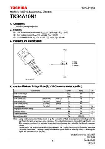
TK34A10N1 MOSFETs Silicon N-channel MOS (U-MOS -H) TK34A10N1 TK34A10N1 TK34A10N1 TK34A10N1 1. Applications 1. Applications 1. Applications 1. Applications Switching Voltage Regulators 2. Features 2. Features 2. Features 2. Features (1) Low drain-source on-resistance RDS(ON) = 7.9 m (typ.) (VGS = 10 V) (2) Low leakage current IDSS = 10 A (max) (VDS = 100 V) (3) Enha
0.3. Size:478K first silicon
ftk3415l.pdf
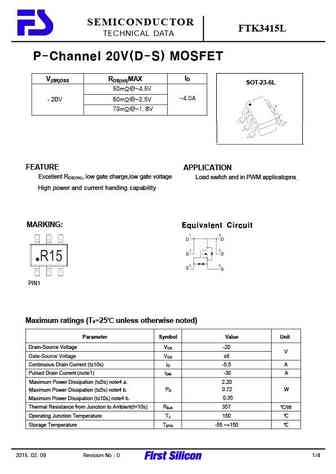
SEMICONDUCTOR FTK3415L TECHNICAL DATA P-Channel 20V(D-S) MOSFET ID V(BR)DSS RDS(on)MAX SOT-23-6L 50m @-4.5V -4.0A -20V 60m @-2.5V 73m @-1. 8V FEATURE APPLICATION Excellent RDS(ON), low gate charge,low gate voltage Load switch and in PWM applicatopns High power and current handing capability MARKING Equivalent Circuit PIN1 Maximum ratings (Ta=25 unless otherwise
0.4. Size:232K first silicon
ftk3400.pdf
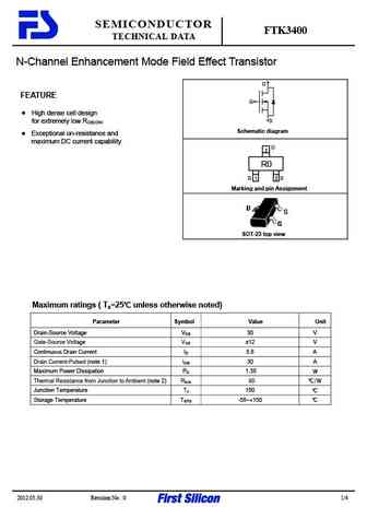
SEMICONDUCTOR FTK3400 TECHNICAL DATA N-Channel Enhancement Mode Field Effect Transistor D FEATURE G High dense cell design for extremely low R S DS(ON) Schematic diagram Exceptional on-resistance and maximum DC current capability D 3 R0 G 1 2 S Marking and pin Assignment SOT-23 top view Maximum ratings ( Ta=25 unless otherwise noted) Parameter Symbol Value Unit
0.5. Size:681K first silicon
ftk3415.pdf
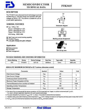
SEMICONDUCTOR FTK3415 TECHNICAL DATA DESCRIPTION D The FTK3415 uses advanced trench technology to provide excellent RDS(ON), low gate charge and operation with gate voltages as low as 1.8V. This device is suitable for use as G a load switch applications. S GENERAL FEATURES Schematic diagram VDS = -20V,ID =-4A RDS(ON)
0.6. Size:305K first silicon
ftk3404.pdf
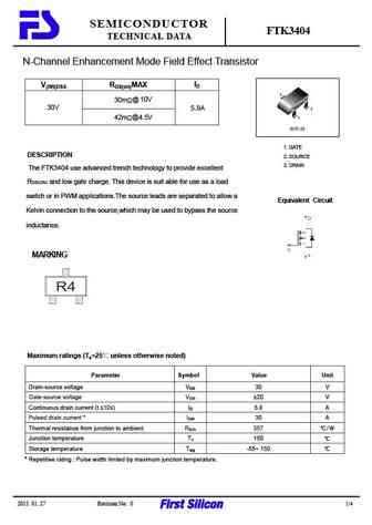
SEMICONDUCTOR FTK3404 TECHNICAL DATA N-Channel Enhancement Mode Field Effect Transistor ID V(BR)DSS RDS(on)MAX 3 30m @ 10V 30V 5.8A 2 1 42m @4.5V SOT 23 1. GATE DESCRIPTION 2. SOURCE 3. DRAIN The FTK3404 use advanced trench technology to provide excellent RDS(ON) and low gate charge. This device is suit able for use as a load switch or in PWM applications.The s
0.7. Size:236K first silicon
ftk3443.pdf
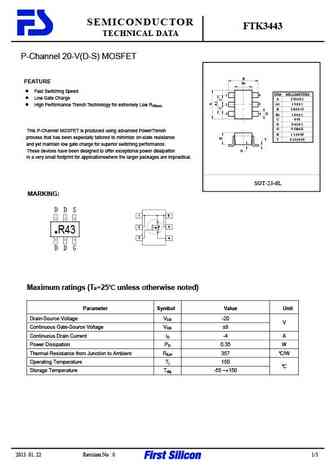
SEMICONDUCTOR FTK3443 TECHNICAL DATA P-Channel 20-V(D-S) MOSFET B FEATURE B1 Fast Switching Speed DIM MILLIMETERS 1 6 Low Gate Charge A 2 92 0 1 2 5 A1 1 9 0 1 High Performance Trench Technology for extremely Low RDS(on) B 2 8 0 15 3 4 D B1 1 6 0 1 C 0 95 D 0 4 0 1 G 0 1MAX This P-Channel MOSFET is produced using advanced PowerTrench H 1 1 0 05 process tha
0.8. Size:380K first silicon
ftk3407l.pdf
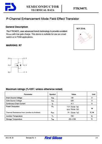
SEMICONDUCTOR FTK3407L TECHNICAL DATA P-Channel Enhancement Mode Field Effect Transistor General Description SOT-23-6L The FTK3407L uses advanced trench technology to provide excellent RDS(on) with low gate charge. This device is suitable for use as a load switch or in PWM applications. MARKING R7 Maximum ratings (Ta=25 unless otherwise noted) Parameter Symbol Value Unit
0.9. Size:229K first silicon
ftk3407.pdf
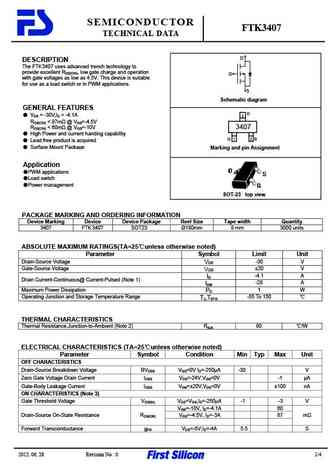
SEMICONDUCTOR FTK3407 TECHNICAL DATA D DESCRIPTION The FTK3407 uses advanced trench technology to provide excellent RDS(ON), low gate charge and operation G with gate voltages as low as 4.5V. This device is suitable for use as a load switch or in PWM applications. S Schematic diagram GENERAL FEATURES D VDS = -30V,ID = -4.1A 3 RDS(ON)
0.10. Size:236K first silicon
ftk3401.pdf
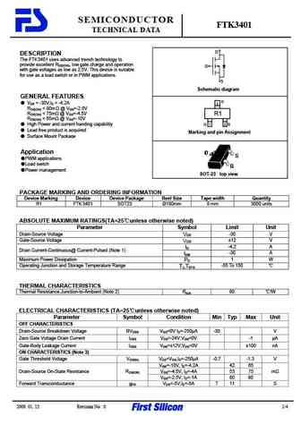
SEMICONDUCTOR FTK3401 TECHNICAL DATA D DESCRIPTION The FTK3401 uses advanced trench technology to provide excellent RDS(ON), low gate charge and operation G with gate voltages as low as 2.5V. This device is suitable for use as a load switch or in PWM applications. S Schematic diagram GENERAL FEATURES D VDS = -30V,ID = -4.2A 3 RDS(ON)
0.11. Size:578K first silicon
ftk3439kd.pdf
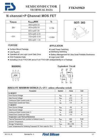
SEMICONDUCTOR FTK3439KD TECHNICAL DATA N channel+P Channel MOS FET ID V(BR)DSS RDS(on)MAX SOT-363 380m @4.5V 450m @2.5V 20V 0.75A 800m @1.8V 520m @-4.5V -20V 700m @-2.5V -0.66A 950m @-1.8V FEATURE APPLICATION Surface Mount Package Load/ Power Switching Interfacing Switching Low RDS(on) Operated at Low Logic Level Gate Drive Battery Management for
0.12. Size:1091K jiejie micro
jmtk340p03a.pdf
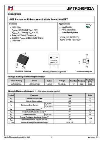
JMTK340P03A Description JMT P-channel Enhancement Mode Power MosFET Features Applications -30V, -20A Load Switch RDS(ON)
0.13. Size:246K inchange semiconductor
tk34e10n1.pdf
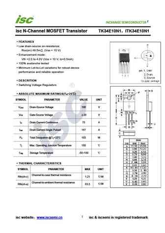
INCHANGE Semiconductor isc N-Channel MOSFET Transistor TK34E10N1 ITK34E10N1 FEATURES Low drain-source on-resistance RDS(on) 9.5m . (VGS = 10 V) Enhancement mode Vth =2.0 to 4.0V (VDS = 10 V, ID=0.5mA) 100% avalanche tested Minimum Lot-to-Lot variations for robust device performance and reliable operation DESCRITION Switching Voltage Regulators ABSOLUTE MAXIM
0.14. Size:253K inchange semiconductor
tk34a10n1.pdf
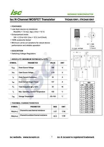
INCHANGE Semiconductor Isc N-Channel MOSFET Transistor TK34A10N1 ITK34A10N1 FEATURES Low drain-source on-resistance RDS(ON) = 7.9 m (typ.) (VGS = 10 V) Enhancement mode Vth = 2.0 to 4.0V (VDS = 10 V, ID=0.5mA) 100% avalanche tested Minimum Lot-to-Lot variations for robust device performance and reliable operation DESCRITION Switching Voltage Regulators ABSOL
Otros transistores... TK28, TK28C, TK30, TK30D, TK31, TK31D, TK33, TK33C, D882, TK34C, TK35, TK35C, TK36, TK36C, TK37, TK37C, TK38
