TK40 Datasheet. Equivalente. Reemplazo. Hoja de especificaciones. Principales características
Número de Parte: TK40 📄📄
Material: Ge
Polaridad de transistor: PNP
ESPECIFICACIONES MÁXIMAS
Disipación total del dispositivo (Pc): 0.2 W
Tensión colector-base (Vcb): 40 V
Tensión colector-emisor (Vce): 20 V
Tensión emisor-base (Veb): 40 V
Corriente del colector DC máxima (Ic): 0.1 A
Temperatura operativa máxima (Tj): 75 °C
CARACTERÍSTICAS ELÉCTRICAS
Transición de frecuencia (fT): 1 MHz
Ganancia de corriente contínua (hFE): 17
Encapsulados: X18
📄📄 Copiar
Búsqueda de reemplazo de TK40
- Selecciónⓘ de transistores por parámetros
TK40 datasheet
0.1. Size:233K toshiba
tk40a06n1.pdf 
TK40A06N1 MOSFETs Silicon N-channel MOS (U-MOS -H) TK40A06N1 TK40A06N1 TK40A06N1 TK40A06N1 1. Applications 1. Applications 1. Applications 1. Applications Switching Voltage Regulators 2. Features 2. Features 2. Features 2. Features (1) Low drain-source on-resistance RDS(ON) = 8.4 m (typ.) (VGS = 10 V) (2) Low leakage current IDSS = 10 A (max) (VDS = 60 V) (3) Enhan
0.2. Size:246K toshiba
tk40e06n1.pdf
TK40E06N1 MOSFETs Silicon N-channel MOS (U-MOS -H) TK40E06N1 TK40E06N1 TK40E06N1 TK40E06N1 1. Applications 1. Applications 1. Applications 1. Applications Switching Voltage Regulators 2. Features 2. Features 2. Features 2. Features (1) Low drain-source on-resistance RDS(ON) = 8.4 m (typ.) (VGS = 10 V) (2) Low leakage current IDSS = 10 A (max) (VDS = 60 V) (3) Enhan
0.3. Size:241K toshiba
tk40p03m1.pdf
TK40P03M1 MOSFETs Silicon N-Channel MOS (U-MOS -H) TK40P03M1 TK40P03M1 TK40P03M1 TK40P03M1 1. Applications 1. Applications 1. Applications 1. Applications DC-DC Converters Desktop PCs 2. Features 2. Features 2. Features 2. Features (1) High-speed switching (2) Low gate charge QSW = 5.7 nC (typ.) (3) Low drain-source on-resistance RDS(ON) = 8.3 m (typ.) (VGS = 10
0.4. Size:197K toshiba
tk40d10j1.pdf
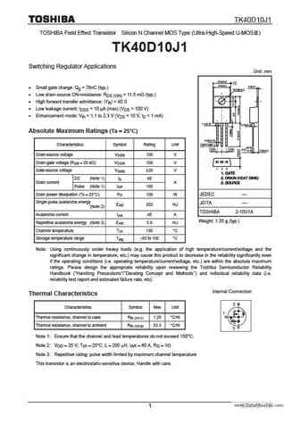
TK40D10J1 www.DataSheet4U.com TOSHIBA Field Effect Transistor Silicon N Channel MOS Type (Ultra-High-Speed U-MOS ) TK40D10J1 Switching Regulator Applications Unit mm 10.0 0.3 A 9.5 0.2 0.6 0.1 Small gate charge Qg = 76nC (typ.) 3.65 0.2 Low drain-source ON-resistance RDS (ON) = 11.5 m (typ.) High forward transfer admittance Yfs = 90 S
0.5. Size:235K toshiba
tk40p04m1.pdf
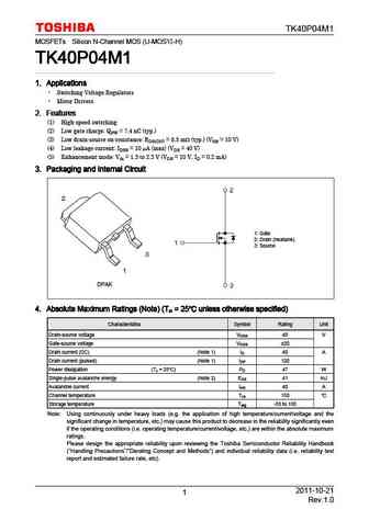
TK40P04M1 MOSFETs Silicon N-Channel MOS (U-MOS -H) TK40P04M1 TK40P04M1 TK40P04M1 TK40P04M1 1. Applications 1. Applications 1. Applications 1. Applications Switching Voltage Regulators Motor Drivers 2. Features 2. Features 2. Features 2. Features (1) High-speed switching (2) Low gate charge QSW = 7.4 nC (typ.) (3) Low drain-source on-resistance RDS(ON) = 8.5 m (t
0.6. Size:177K toshiba
tk40a10j1.pdf
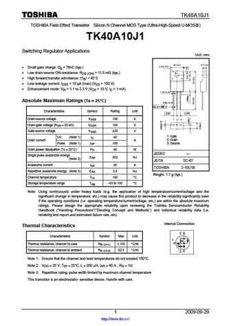
TK40A10J1 TOSHIBA Field Effect Transistor Silicon N Channel MOS Type (Ultra-High-Speed U-MOS ) TK40A10J1 Switching Regulator Applications Unit mm Small gate charge Qg = 76nC (typ.) Low drain-source ON-resistance RDS (ON) = 11.5 m (typ.) High forward transfer admittance Yfs = 90 S Low leakage current IDSS = 10 A (max) (VDS = 100 V) Enhancement m
0.7. Size:237K toshiba
tk40j20d.pdf

TK40J20D MOSFETs Silicon N-Channel MOS ( -MOS ) TK40J20D TK40J20D TK40J20D TK40J20D 1. Applications 1. Applications 1. Applications 1. Applications Switching Voltage Regulators 2. Features 2. Features 2. Features 2. Features (1) Low drain-source on-resistance RDS(ON) = 0.0374 (typ.) (2) Low leakage current IDSS = 10 A (max) (VDS = 200 V) (3) Enhancement mode Vth
0.8. Size:243K toshiba
tk40s10k3z.pdf
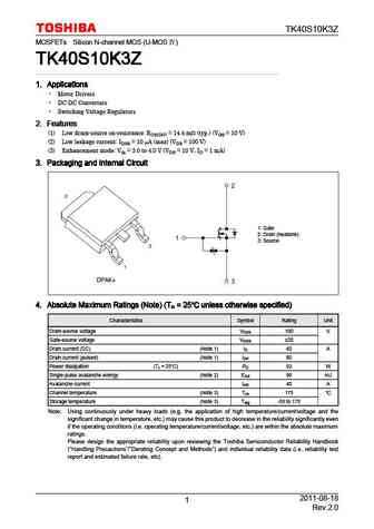
TK40S10K3Z MOSFETs Silicon N-channel MOS (U-MOS ) TK40S10K3Z TK40S10K3Z TK40S10K3Z TK40S10K3Z 1. Applications 1. Applications 1. Applications 1. Applications Motor Drivers DC-DC Converters Switching Voltage Regulators 2. Features 2. Features 2. Features 2. Features (1) Low drain-source on-resistance RDS(ON) = 14.4 m (typ.) (VGS = 10 V) (2) Low leakage curren
0.9. Size:243K toshiba
tk40m60u.pdf
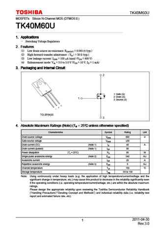
TK40M60U MOSFETs Silicon N-Channel MOS (DTMOS ) TK40M60U TK40M60U TK40M60U TK40M60U 1. Applications 1. Applications 1. Applications 1. Applications Switching Voltage Regulators 2. Features 2. Features 2. Features 2. Features (1) Low drain-source on-resistance RDS(ON) = 0.065 (typ.) (2) High forward transfer admittance Yfs = 30 S (typ.) (3) Low leakage current IDS
0.10. Size:220K toshiba
tk40f08k3.pdf
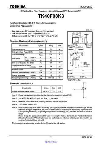
TK40F08K3 TOSHIBA Field Effect Transistor Silicon N Channel MOS Type (U-MOSIV) TK40F08K3 Swiching Regulator, DC-DC Converter Applications Motor Drive Applications Unit mm Low drain-source ON-resistance RDS (ON) = 6.5 m (typ.) 10.0 0.3 Low leakage current IDSS = 10 A (max) (VDS = 75 V) 0.4 0.1 9.5 0.2 Enhancement-model Vth = 3.0 to 4.0 V (VDS = 10
0.12. Size:211K toshiba
tk40x10j1.pdf
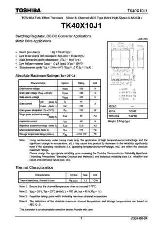
TK40X10J1 TOSHIBA Field Effect Transistor Silicon N Channel MOS Type (Ultra-High-Speed U-MOS ) TK40X10J1 Switching Regulator, DC-DC Converter Applications Unit mm Motor Drive Applications Small gate charge Qg = 59 nC (typ.) Low drain-source ON-resistance RDS (ON) = 15 m (typ.) High forward transfer admittance Yfs = 60 S (typ.) Low leakage current ID
0.13. Size:237K toshiba
tk40j60u.pdf
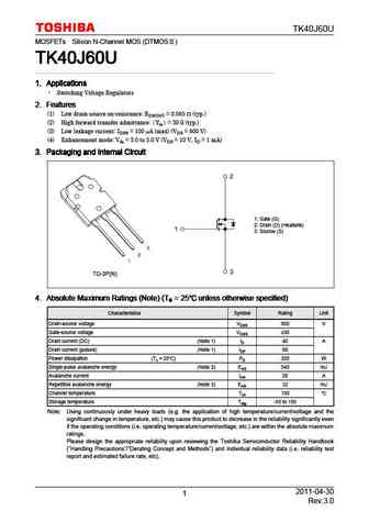
TK40J60U MOSFETs Silicon N-Channel MOS (DTMOS ) TK40J60U TK40J60U TK40J60U TK40J60U 1. Applications 1. Applications 1. Applications 1. Applications Switching Voltage Regulators 2. Features 2. Features 2. Features 2. Features (1) Low drain-source on-resistance RDS(ON) = 0.065 (typ.) (2) High forward transfer admittance Yfs = 30 S (typ.) (3) Low leakage current IDS
0.14. Size:233K toshiba
tk40a10n1.pdf
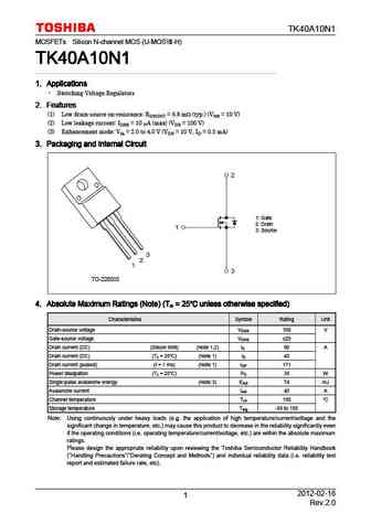
TK40A10N1 MOSFETs Silicon N-channel MOS (U-MOS -H) TK40A10N1 TK40A10N1 TK40A10N1 TK40A10N1 1. Applications 1. Applications 1. Applications 1. Applications Switching Voltage Regulators 2. Features 2. Features 2. Features 2. Features (1) Low drain-source on-resistance RDS(ON) = 6.8 m (typ.) (VGS = 10 V) (2) Low leakage current IDSS = 10 A (max) (VDS = 100 V) (3) Enha
0.15. Size:253K toshiba
tk40e10n1.pdf
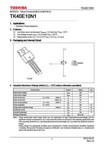
TK40E10N1 MOSFETs Silicon N-channel MOS (U-MOS -H) TK40E10N1 TK40E10N1 TK40E10N1 TK40E10N1 1. Applications 1. Applications 1. Applications 1. Applications Switching Voltage Regulators 2. Features 2. Features 2. Features 2. Features (1) Low drain-source on-resistance RDS(ON) = 6.8 m (typ.) (VGS = 10 V) (2) Low leakage current IDSS = 10 A (max) (VDS = 100 V) (3) Enha
0.16. Size:202K toshiba
tk40a10k3.pdf
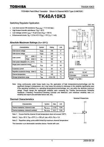
TK40A10K3 TOSHIBA Field Effect Transistor Silicon N Channel MOS Type (U-MOS ) TK40A10K3 Switching Regulator Application Unit mm Low drain-source ON resistance RDS (ON) = 11.5 m (typ.) High forward transfer admittance Yfs = 80 S Low leakage current IDSS = 10 A (max) (VDS = 100 V) Enhancement-mode Vth = 2.0 to 4.0 V (VDS = 10 V, ID = 1 mA) Absolute M
0.17. Size:224K toshiba
tk40j60t.pdf
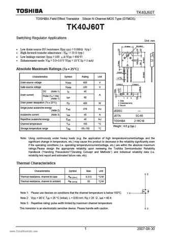
TK40J60T www.DataSheet4U.com TOSHIBA Field Effect Transistor Silicon N Channel MOS Type (DTMOS) TK40J60T Switching Regulator Applications Unit mm 3.2 0.2 15.9max. Low drain-source ON resistance RDS (ON) = 0.068 (typ.) High forward transfer admittance Yfs = 25 S (typ.) Low leakage current IDSS = 100 A (VDS = 600 V) Enhancement-mode Vth = 3.0
0.18. Size:258K toshiba
tk40s06n1l.pdf
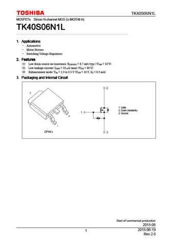
TK40S06N1L MOSFETs Silicon N-channel MOS (U-MOS -H) TK40S06N1L TK40S06N1L TK40S06N1L TK40S06N1L 1. Applications 1. Applications 1. Applications 1. Applications Automotive Motor Drivers Switching Voltage Regulators 2. Features 2. Features 2. Features 2. Features (1) Low drain-source on-resistance RDS(ON) = 8.7 m (typ.) (VGS = 10 V) (2) Low leakage current IDS
0.19. Size:96K samhop
stk400.pdf
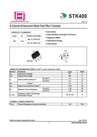
Gre r r P Pr Pr Pro STK400 a S mHop Microelectronics C orp. Ver 1.0 N-Channel Enhancement Mode Field Effect Transistor FEATURES PRODUCT SUMMARY Super high dense cell design for low RDS(ON). RDS(ON) (m ) Max VDSS ID Rugged and reliable. 390 @ VGS=10V Suface Mount Package. 40V 1.3A 550 @ VGS=4.5V ESD Protected. D D G S D SOT-89 G S (TA=25 C unless otherwise noted)
0.20. Size:373K first silicon
ftk40p04d.pdf
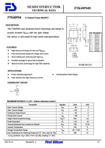
SEMICONDUCTOR FTK40P04D TECHNICAL DATA FTK40P04 P-Channel Power MOSFET A I DESCRIPTION C J The FTK40P04 uses advanced trench technology and design to provide excellent RDS(ON) with low gate charge. DIM MILLIMETERS A 6 50 0 2 B 5 60 0 2 This device is well suited for high current load applications. C 5 20 0 2 D 1 50 0 2 E 2 70 0 2 F 2 30 0 1 H H 1 00 MA
0.21. Size:578K first silicon
ftk4004.pdf
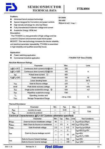
SEMICONDUCTOR FTK4004 TECHNICAL DATA Feathers ID=200A Advanced trench process technology BV=40V Special designed for Convertors and power controls Rdson=4 m max. High density cell design for ultra low Rdson Fully characterized Avalanche voltage and current Avalanche Energy 100% test Description The FTK4004 is a new generation of high voltage and low curre
0.22. Size:342K first silicon
ftk40n10d.pdf
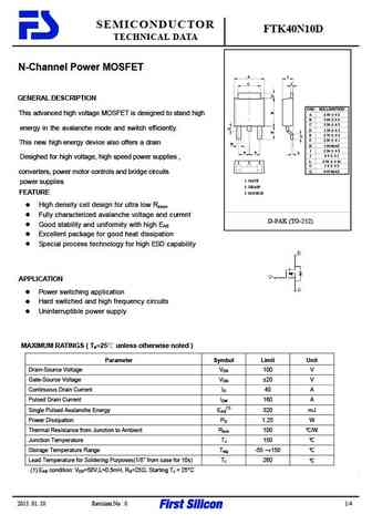
SEMICONDUCTOR FTK40N10D TECHNICAL DATA N-Channel Power MOSFET A I C J GENERAL DESCRIPTION DIM MILLIMETERS This advanced high voltage MOSFET is designed to stand high A 6 50 0 2 B 5 60 0 2 C 5 20 0 2 energy in the avalanche mode and switch efficiently. D 1 50 0 2 E 2 70 0 2 F 2 30 0 1 This new high energy device also offers a drain H H 1 00 MAX I 2 30
0.23. Size:375K first silicon
ftk4015d.pdf
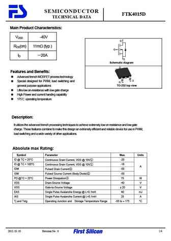
SEMICONDUCTOR FTK4015D TECHNICAL DATA Main Product Characteristics VDSS -40V D RDS(on) 11m (typ.) G ID 20A S Schematic diagram D Features and Benefits Advanced trench MOSFET process technology S Special designed for PWM, load switching and G TO-252 top view general purpose applications Ultra low on-resistance with low gate charge High Power and current
0.24. Size:881K jiejie micro
jmtk4005a.pdf
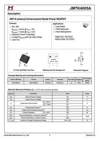
JMTK4005A Description JMT N-channel Enhancement Mode Power MOSFET Features Applications 40V, 80A Load Switch RDS(ON)
0.25. Size:568K jiejie micro
jmtk4004a.pdf
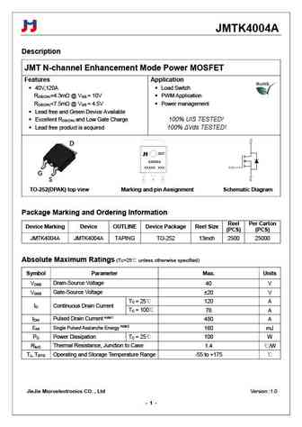
JMTK4004A Description JMT N-channel Enhancement Mode Power MOSFET Features Application 40V,120A Load Switch R
0.26. Size:1229K jiejie micro
jmtk4006a.pdf
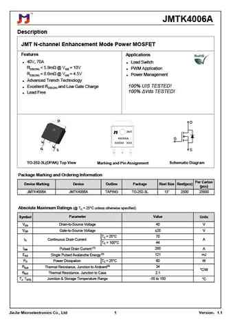
JMTK4006A Description JMT N-channel Enhancement Mode Power MOSFET Features Applications 40V, 70A Load Switch RDS(ON)
0.27. Size:1425K cn vbsemi
tk40p04m.pdf
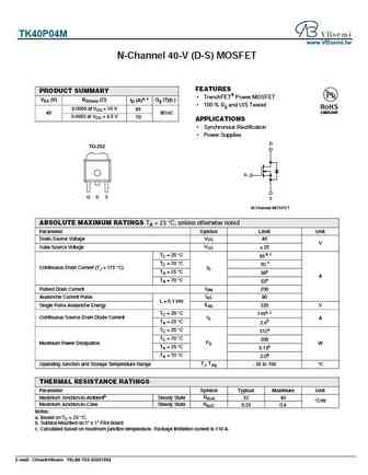
TK40P04M www.VBsemi.tw N-Channel 40-V (D-S) MOSFET FEATURES PRODUCT SUMMARY TrenchFET Power MOSFET VDS (V) RDS(on) ( ) ID (A)a, c Qg (Typ.) 100 % Rg and UIS Tested RoHS 0.0050 at VGS = 10 V 85 COMPLIANT 40 80 nC 0.0065 at VGS = 4.5 V 70 APPLICATIONS Synchronous Rectification Power Supplies D TO-252 G G D S S N-Channel MOSFET ABSOLUTE MAXIMUM RA
0.28. Size:252K inchange semiconductor
tk40a06n1.pdf
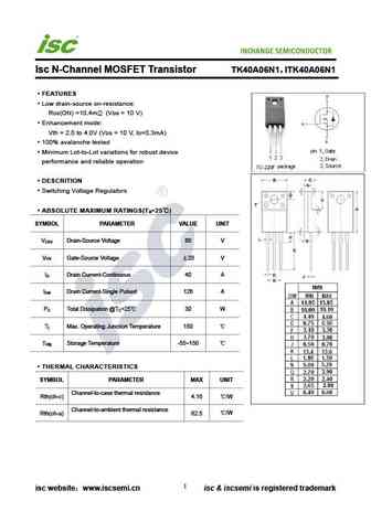
INCHANGE Semiconductor Isc N-Channel MOSFET Transistor TK40A06N1 ITK40A06N1 FEATURES Low drain-source on-resistance RDS(ON) =10.4m (VGS = 10 V) Enhancement mode Vth = 2.0 to 4.0V (VDS = 10 V, ID=0.3mA) 100% avalanche tested Minimum Lot-to-Lot variations for robust device performance and reliable operation DESCRITION Switching Voltage Regulators ABSOLUTE MAXI
0.29. Size:238K inchange semiconductor
tk40j60u.pdf
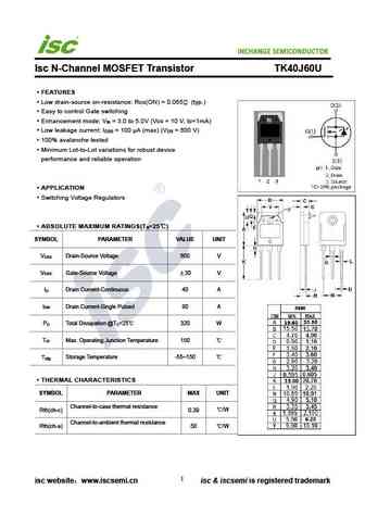
INCHANGE Semiconductor Isc N-Channel MOSFET Transistor TK40J60U FEATURES Low drain-source on-resistance RDS(ON) = 0.065 (typ.) Easy to control Gate switching Enhancement mode V = 3.0 to 5.0V (VDS = 10 V, ID=1mA) th Low leakage current I = 100 A (max) (V = 600 V) DSS DS 100% avalanche tested Minimum Lot-to-Lot variations for robust device performance and reliable
0.30. Size:252K inchange semiconductor
tk40a10n1.pdf
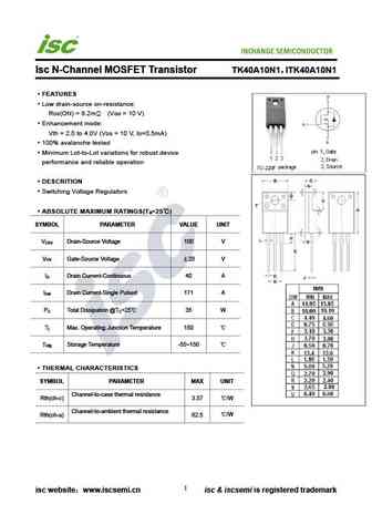
INCHANGE Semiconductor Isc N-Channel MOSFET Transistor TK40A10N1 ITK40A10N1 FEATURES Low drain-source on-resistance RDS(ON) = 8.2m (VGS = 10 V) Enhancement mode Vth = 2.0 to 4.0V (VDS = 10 V, ID=0.5mA) 100% avalanche tested Minimum Lot-to-Lot variations for robust device performance and reliable operation DESCRITION Switching Voltage Regulators ABSOLUTE MAXI
0.31. Size:232K inchange semiconductor
tk40e10n1.pdf
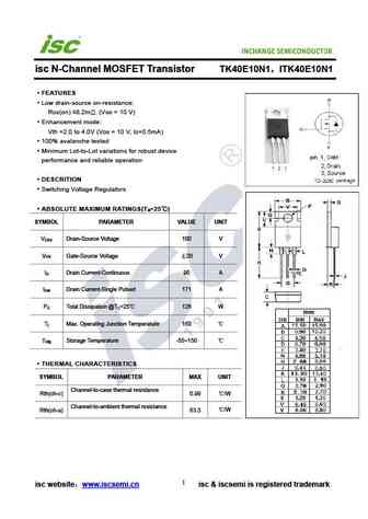
INCHANGE Semiconductor isc N-Channel MOSFET Transistor TK40E10N1 ITK40E10N1 FEATURES Low drain-source on-resistance RDS(on) 8.2m . (VGS = 10 V) Enhancement mode Vth =2.0 to 4.0V (VDS = 10 V, ID=0.5mA) 100% avalanche tested Minimum Lot-to-Lot variations for robust device performance and reliable operation DESCRITION Switching Voltage Regulators ABSOLUTE MAXIM
Otros transistores... TK35, TK35C, TK36, TK36C, TK37, TK37C, TK38, TK38C, 2SD1047, TK400A, TK401A, TK402A, TK403A, TK40A, TK40C, TK41, TK41C