2N54 Datasheet. Equivalente. Reemplazo. Hoja de especificaciones. Principales características
Número de Parte: 2N54 📄📄
Material: Ge
Polaridad de transistor: PNP
ESPECIFICACIONES MÁXIMAS
Disipación total del dispositivo (Pc): 0.2 W
Tensión colector-base (Vcb): 45 V
Corriente del colector DC máxima (Ic): 0.01 A
Temperatura operativa máxima (Tj): 60 °C
CARACTERÍSTICAS ELÉCTRICAS
Transición de frecuencia (fT): 0.5 MHz
Ganancia de corriente contínua (hFE): 19
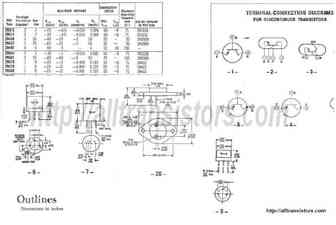
Encapsulados: TO50-3
📄📄 Copiar
Búsqueda de reemplazo de 2N54
- Selecciónⓘ de transistores por parámetros
2N54 datasheet
2n5400 2n5401.pdf
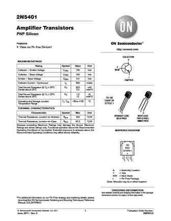
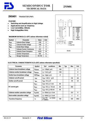
MOTOROLA Order this document SEMICONDUCTOR TECHNICAL DATA by 2N5400/D Amplifier Transistors 2N5400 PNP Silicon * 2N5401 *Motorola Preferred Device COLLECTOR 3 2 BASE 1 EMITTER 1 2 3 MAXIMUM RATINGS Rating Symbol 2N5400 2N5401 Unit CASE 29 04, STYLE 1 TO 92 (TO 226AA) Collector Emitter Voltage VCEO 120 150 Vdc Collector Base Voltage VCBO 130 160 Vdc Emitter B
2n5457re.pdf
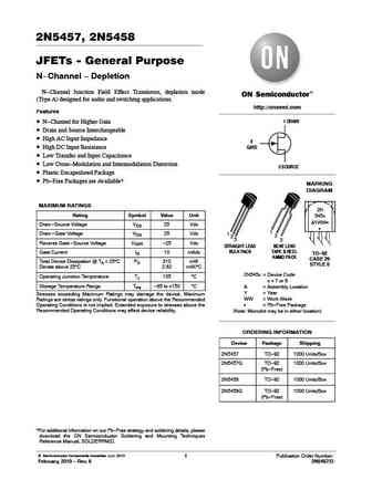
MOTOROLA Order this document SEMICONDUCTOR TECHNICAL DATA by 2N5457/D JFETs General Purpose 2N5457 N Channel Depletion 1 DRAIN *Motorola Preferred Device 3 GATE 2 SOURCE MAXIMUM RATINGS Rating Symbol Value Unit 1 2 3 Drain Source Voltage VDS 25 Vdc Drain Gate Voltage VDG 25 Vdc CASE 29 04, STYLE 5 Reverse Gate Source Voltage VGSR 25 Vdc TO 92 (TO 226AA)
2n5401.pdf
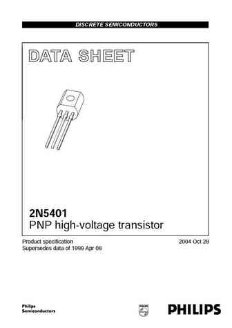
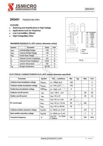
DISCRETE SEMICONDUCTORS DATA SHEET book, halfpage M3D186 2N5401 PNP high-voltage transistor Product specification 2004 Oct 28 Supersedes data of 1999 Apr 08 Philips Semiconductors Product specification PNP high-voltage transistor 2N5401 FEATURES PINNING Low current (max. 300 mA) PIN DESCRIPTION High voltage (max. 150 V). 1 collector 2 base APPLICATIONS 3 emitter G
2n5415 2n5416 cnv 2.pdf
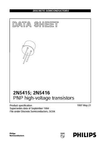
DISCRETE SEMICONDUCTORS DATA SHEET book, halfpage M3D111 2N5415; 2N5416 PNP high-voltage transistors 1997 May 21 Product specification Supersedes data of September 1994 File under Discrete Semiconductors, SC04 Philips Semiconductors Product specification PNP high-voltage transistors 2N5415; 2N5416 FEATURES PINNING Low current (max. 200 mA) PIN DESCRIPTION High voltage (m
2n5415 2n5416.pdf

DISCRETE SEMICONDUCTORS DATA SHEET book, halfpage M3D111 2N5415; 2N5416 PNP high-voltage transistors 1997 May 21 Product specification Supersedes data of September 1994 File under Discrete Semiconductors, SC04 Philips Semiconductors Product specification PNP high-voltage transistors 2N5415; 2N5416 FEATURES PINNING Low current (max. 200 mA) PIN DESCRIPTION High voltage (m
2n5401hr.pdf
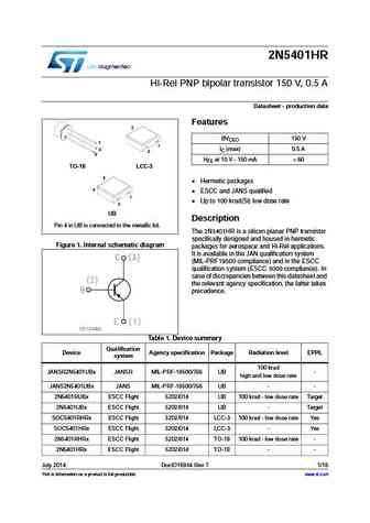
2N5401HR Hi-Rel PNP bipolar transistor 150 V, 0.5 A Datasheet - production data Features 3 BVCEO 150 V 1 1 IC (max) 0.5 A 2 2 3 HFE at 10 V - 150 mA > 60 TO-18 LCC-3 3 Hermetic packages 4 ESCC and JANS qualified 1 Up to 100 krad(Si) low dose rate 2 UB Description Pin 4 in UB is connected to the metallic lid. The 2N5401HR is a silicon planar PNP transistor
2n5415 2n5416.pdf

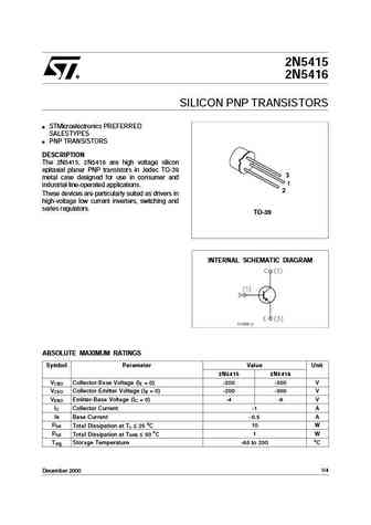
2N5415 2N5416 SILICON PNP TRANSISTORS STMicroelectronics PREFERRED SALESTYPES PNP TRANSISTORS DESCRIPTION The 2N5415, 2N5416 are high voltage silicon epitaxial planar PNP transistors in Jedec TO-39 metal case designed for use in consumer and industrial line-operated applications. These devices are particularly suited as drivers in high-voltage low current inverters, switching
2n5415 2n5416 .pdf
2N5415 2N5416 SILICON PNP TRANSISTORS STMicroelectronics PREFERRED SALESTYPES PNP TRANSISTORS DESCRIPTION The 2N5415, 2N5416 are high voltage silicon epitaxial planar PNP transistors in Jedec TO-39 metal case designed for use in consumer and industrial line-operated applications. These devices are particularly suited as drivers in high-voltage low current inverters, switching
2n5484 2n5485 2n5486 mmbf5484 mmbf5485 mmbf5486.pdf
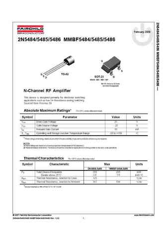
February 2009 2N5484/5485/5486 MMBF5484/5485/5486 2007 Fairchild Semiconductor Corporation www.fairchildsemi.com 2N5484/5485/5486 MMBF5484/5485/5486 Rev. 1.0.0 1 2N5484/5485/5486 MMBF5484/5485/5486 2007 Fairchild Semiconductor Corporation www.fairchildsemi.com Rev. 1.0.0 2 2007 Fairchild Semiconductor Corporation www.fairchildsemi.com Rev. 1.0.0 3 2007
2n5401 mmbt5401.pdf
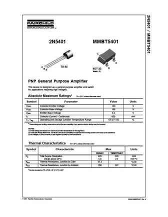
2N5401 MMBT5401 C E C TO-92 B B SOT-23 E Mark 2L PNP General Purpose Amplifier This device is designed as a general purpose amplifier and switch for applications requiring high voltages. Absolute Maximum Ratings* TA = 25 C unless otherwise noted Symbol Parameter Value Units VCEO Collector-Emitter Voltage 150 V VCBO Collector-Base Voltage 160 V VEBO Emitter-Base Voltage 5.0 V I
2n5457 2n5458 2n5459 mmbf5457 mmbf5458 mmbf5459.pdf
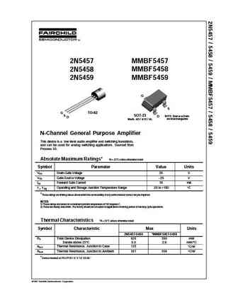
2N5457 MMBF5457 2N5458 MMBF5458 2N5459 MMBF5459 G S TO-92 G S SOT-23 NOTE Source & Drain D D are interchangeable Mark 6D / 61S / 6L N-Channel General Purpose Amplifier This device is a low level audio amplifier and switching transistors, and can be used for analog switching applications. Sourced from Process 55. Absolute Maximum Ratings* TA = 25 C unless otherwise noted S
2n5484 mmbf5484.pdf
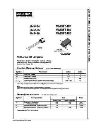
2N5484 MMBF5484 2N5485 MMBF5485 2N5486 MMBF5486 G S G TO-92 S SOT-23 D D Mark 6B / 6M / 6H NOTE Source & Drain are interchangeable N-Channel RF Amplifier This device is designed primarily for electronic switching applications such as low On Resistance analog switching. Sourced from Process 50. Absolute Maximum Ratings* TA = 25 C unless otherwise noted Symbol Parameter Value
2n5460 2n5461 2n5462 mmbf5460 mmbf5461 mmbf5462.pdf
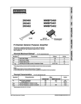
2N5460 MMBF5460 2N5461 MMBF5461 2N5462 MMBF5462 G S G TO-92 D SOT-23 NOTE Source & Drain S Mark 6E / 61U / 61V are interchangeable D P-Channel General Purpose Amplifier This device is designed primarily for low level audio and general purpose applications with high impedance signal sources. Sourced from Process 89. Absolute Maximum Ratings* TA = 25 C unless otherwise noted -
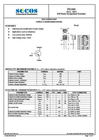
2n5400.pdf
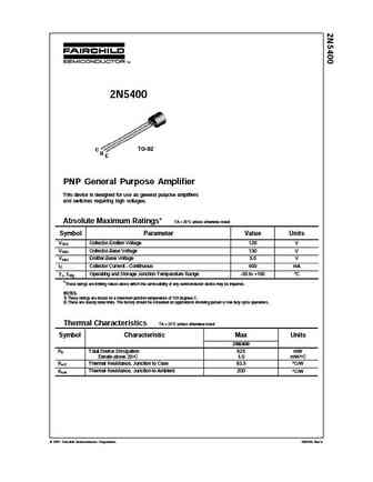
2N5400 C TO-92 B E PNP General Purpose Amplifier This device is designed for use as general purpose amplifiers and switches requiring high voltages. Absolute Maximum Ratings* TA = 25 C unless otherwise noted Symbol Parameter Value Units VCEO Collector-Emitter Voltage 120 V VCBO Collector-Base Voltage 130 V VEBO Emitter-Base Voltage 5.0 V ICCollector Current - Continuous600mA Oper
2n5401.pdf
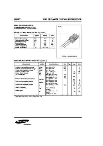
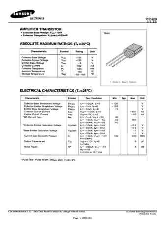
2N5401 PNP EPITAXIAL SILICON TRANSISTOR AMPLIFIER TRANSISTOR TO-92 Collector-Emitter Voltage VCEO= 150V Collector Dissipation PC (max)=625mW ABSOLUTE MAXIMUM RATINGS (T =25 ) A Characteristic Symbol Rating Unit Collector-Base Voltage VCBO -160 V Collector-Emitter Voltage VCEO -150 V Emitter-Base Voltage VEBO -5 V Collector Current IC -600 mA Collector Dissipation PC 625 m
2n5400.pdf
2N5400 S/S TR CD-ROM(Edition.1.1) This Data Sheet is subject to change without notice. (C) 1994 Samsung Electronics Printed in Korea. Page 1 (2N5400)
2n5484 sst5484 2n5485 sst5485 2n5486 sst5486.pdf
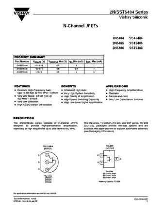
2N/SST5484 Series Vishay Siliconix N-Channel JFETs 2N5484 SST5484 2N5485 SST5485 2N5486 SST5486 PRODUCT SUMMARY Part Number VGS(off) (V) V(BR)GSS Min (V) gfs Min (mS) IDSS Min (mA) 2N/SST5484 -0.3 to -3 -25 3 1 2N/SST5485 -0.5 to -4 -25 3.5 4 2N/SST5486 -2 to -6 -25 4 8 FEATURES BENEFITS APPLICATIONS D Excellent High-Frequency Gain D Wideband High Gain D High-Frequency Amplifier/Mi
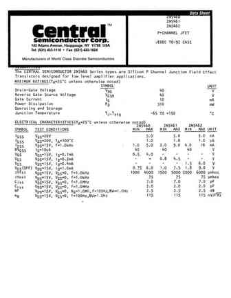
2n5460 sst5460 2n5461 sst5461 2n5462 sst5462.pdf
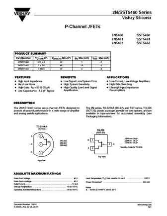
2N/SST5460 Series Vishay Siliconix P-Channel JFETs 2N5460 SST5460 2N5461 SST5461 2N5462 SST5462 PRODUCT SUMMARY Part Number VGS(off) (V) V(BR)GSS Min (V) gfs Min (mS) IDSS Min (mA) 2N/SST5460 0.75 to 6 40 1 1 2N/SST5461 1 to 7.5 40 1.5 2 2N/SST5462 1.8 to 9 40 2 4 FEATURES BENEFITS APPLICATIONS D High Input Impedance D Low Signal Loss/System Error D Low-Current, Low-Voltage
2n5432 2n5433 2n5434.pdf
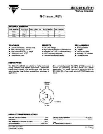
2N5432/5433/5434 Vishay Siliconix N-Channel JFETs PRODUCT SUMMARY Part Number VGS(off) (V) rDS(on) Max (W) ID(off) Typ (pA) tON Typ (ns) 2N5432 4 to 10 5 10 2.5 2N5433 3 to 9 7 10 2.5 2N5434 1 to 4 10 10 2.5 FEATURES BENEFITS APPLICATIONS D Low On-Resistance 2N5432
2n5460 2n5461 2n5462.pdf
145 Adams Avenue, Hauppauge, NY 11788 USA Tel (631) 435-1110 Fax (631) 435-1824
2n5457 2n5458 2n5459.pdf
145 Adams Avenue, Hauppauge, NY 11788 USA Tel (631) 435-1110 Fax (631) 435-1824
2n5400 2n5401.pdf
145 Adams Avenue, Hauppauge, NY 11788 USA Tel (631) 435-1110 Fax (631) 435-1824
2n5415 2n5416 2.pdf
145 Adams Avenue, Hauppauge, NY 11788 USA Tel (631) 435-1110 Fax (631) 435-1824
2n5484 2n5485 2n5486.pdf
145 Adams Avenue, Hauppauge, NY 11788 USA Tel (631) 435-1110 Fax (631) 435-1824
2n5490 2n5492 2n5494 2n5496.pdf
145 Adams Avenue, Hauppauge, NY 11788 USA Tel (631) 435-1110 Fax (631) 435-1824
2n5401.pdf
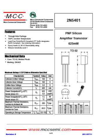
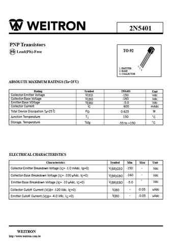
2N5401 MCC TM Micro Commercial Components ELECTRICAL CHARACTERISTICS (TA = 25 C unless otherwise noted) Characteristic Symbol Min Max Unit OFF CHARACTERISTICS Collector Emitter Breakdown Voltage(1) V(BR)CEO Vdc (IC = 1.0 mAdc, IB = 0) 150 Collector Base Breakdown Voltage V(BR)CBO Vdc (IC = 100 mAdc, IE = 0) 160 Emitter Base Breakdown Voltage V(BR)EBO 5.0 Vdc (IE
2n5460 2n5461 2n5462.pdf
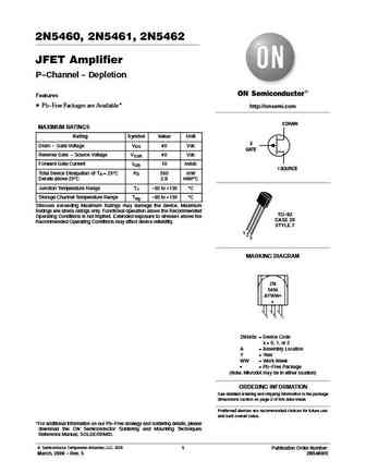
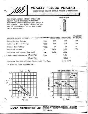
2N5460, 2N5461, 2N5462 JFET Amplifier P-Channel - Depletion Features Pb-Free Packages are Available* http //onsemi.com 2 DRAIN MAXIMUM RATINGS Rating Symbol Value Unit 3 Drain - Gate Voltage VDG 40 Vdc GATE Reverse Gate - Source Voltage VGSR 40 Vdc Forward Gate Current IG(f) 10 mAdc 1 SOURCE Total Device Dissipation @ TA = 25 C PD 350 mW Derate above 25 C 2.8 mW/ C Junct
2n5401rlrag.pdf
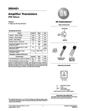
2N5401 Amplifier Transistors PNP Silicon Features These are Pb-Free Devices* http //onsemi.com COLLECTOR 3 MAXIMUM RATINGS Rating Symbol Value Unit 2 BASE Collector - Emitter Voltage VCEO 150 Vdc Collector - Base Voltage VCBO 160 Vdc 1 Emitter - Base Voltage VEBO 5.0 Vdc EMITTER Collector Current - Continuous IC 600 mAdc Total Device Dissipation @ TA = 25 C PD 625 mW Der
2n5401g.pdf

2N5401 Amplifier Transistors PNP Silicon Features These are Pb-Free Devices* http //onsemi.com COLLECTOR 3 MAXIMUM RATINGS Rating Symbol Value Unit 2 BASE Collector - Emitter Voltage VCEO 150 Vdc Collector - Base Voltage VCBO 160 Vdc 1 Emitter - Base Voltage VEBO 5.0 Vdc EMITTER Collector Current - Continuous IC 600 mAdc Total Device Dissipation @ TA = 25 C PD 625 mW Der
2n5486.pdf
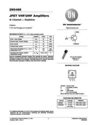
2N5486 JFET VHF/UHF Amplifiers N-Channel Depletion Features Pb-Free Packages are Available* http //onsemi.com 1 DRAIN MAXIMUM RATINGS (TJ = 25 C unless otherwise noted) Rating Symbol Value Unit 3 GATE Drain-Gate Voltage VDG 25 Vdc Reverse Gate-Source Voltage VGSR 25 Vdc 2 SOURCE Drain Current ID 30 mAdc Forward Gate Current IG(f) 10 mAdc Total Device Dissipation @ TC =
2n5401-d.pdf
2N5401 Amplifier Transistors PNP Silicon Features These are Pb-Free Devices* http //onsemi.com COLLECTOR 3 MAXIMUM RATINGS Rating Symbol Value Unit 2 BASE Collector - Emitter Voltage VCEO 150 Vdc Collector - Base Voltage VCBO 160 Vdc 1 Emitter - Base Voltage VEBO 5.0 Vdc EMITTER Collector Current - Continuous IC 600 mAdc Total Device Dissipation @ TA = 25 C PD 625 mW Der

2n5401.pdf
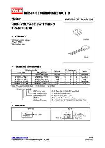
UNISONIC TECHNOLOGIES CO., LTD 2N5401 PNP SILICON TRANSISTOR HIGH VOLTAGE SWITCHING TRANSISTOR FEATURES * Collector-emitter voltage VCEO = -150V * High current gain, ORDERING INFORMATION Ordering Number Pin Assignment Package Packing Lead Free Halogen Free 1 2 3 - 2N5401G-x-AB3-R SOT-89 B C E Tape Reel 2N5401L-x-T92-B 2N5401G-x-T92-B TO-92 E B C Tape Box 2N5401
2n5401.pdf
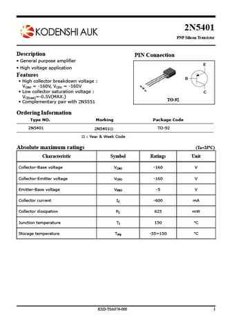
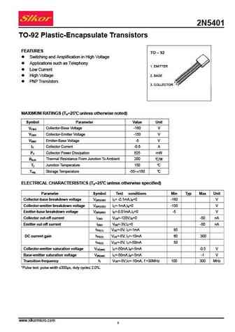
2N5401 PNP Silicon Transistor Description PIN Connection General purpose amplifier E High voltage application Features B High collector breakdown voltage VCBO = -160V, VCEO = -160V Low collector saturation voltage C VCE(sat)=-0.5V(MAX.) TO-92 Complementary pair with 2N5551 Ordering Information Type NO. Marking Package Code 2N5401 TO-9
2n5401n.pdf
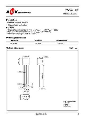
2N5401N Semiconductor Semiconductor PNP Silicon Transistor Description General purpose amplifier High voltage application Features High collector breakdown voltage VCBO = -160V, VCEO = -160V Low collector saturation voltage VCE(sat)=-0.5V(MAX.) Complementary pair with 2N5551N Ordering Information Type NO. Marking Package Code 2N5401N 2N5401 T
2n5415u4.pdf

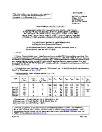
INCH-POUND The documentation and process conversion measures necessary to comply with this document shall be MIL-PRF-19500/485N completed by 10 September 2013. 10 June 2013 SUPERSEDING MIL-PRF-19500/485M 1 June 2010 PERFORMANCE SPECIFICATION SHEET SEMICONDUCTOR DEVICE, TRANSISTOR, PNP, SILICON, LOW-POWER TYPES 2N5415, 2N5415S, 2N5415UA, 2N5415U4, 2N5416, 2N5416S, 2N5416UA
2n5416ua.pdf

INCH-POUND The documentation and process conversion measures necessary to comply with this document shall be MIL-PRF-19500/485N completed by 10 September 2013. 10 June 2013 SUPERSEDING MIL-PRF-19500/485M 1 June 2010 PERFORMANCE SPECIFICATION SHEET SEMICONDUCTOR DEVICE, TRANSISTOR, PNP, SILICON, LOW-POWER TYPES 2N5415, 2N5415S, 2N5415UA, 2N5415U4, 2N5416, 2N5416S, 2N5416UA
2n5416u4.pdf
INCH-POUND The documentation and process conversion measures necessary to comply with this document shall be MIL-PRF-19500/485N completed by 10 September 2013. 10 June 2013 SUPERSEDING MIL-PRF-19500/485M 1 June 2010 PERFORMANCE SPECIFICATION SHEET SEMICONDUCTOR DEVICE, TRANSISTOR, PNP, SILICON, LOW-POWER TYPES 2N5415, 2N5415S, 2N5415UA, 2N5415U4, 2N5416, 2N5416S, 2N5416UA
2n5415ua.pdf

INCH-POUND The documentation and process conversion measures necessary to comply with this document shall be MIL-PRF-19500/485N completed by 10 September 2013. 10 June 2013 SUPERSEDING MIL-PRF-19500/485M 1 June 2010 PERFORMANCE SPECIFICATION SHEET SEMICONDUCTOR DEVICE, TRANSISTOR, PNP, SILICON, LOW-POWER TYPES 2N5415, 2N5415S, 2N5415UA, 2N5415U4, 2N5416, 2N5416S, 2N5416UA
2n5416s.pdf

INCH-POUND The documentation and process conversion measures necessary to comply with this document shall be MIL-PRF-19500/485N completed by 10 September 2013. 10 June 2013 SUPERSEDING MIL-PRF-19500/485M 1 June 2010 PERFORMANCE SPECIFICATION SHEET SEMICONDUCTOR DEVICE, TRANSISTOR, PNP, SILICON, LOW-POWER TYPES 2N5415, 2N5415S, 2N5415UA, 2N5415U4, 2N5416, 2N5416S, 2N5416UA
2n3904 2n3906 2n5401 2n5551 2sa1271 2sa1273 2sa1275 2sa1276 2sa1366 2sa1657 2sa1658 2sb1366 2sb988 2sc3190 2sc3191 2sc3192.pdf
2n5401csm.pdf
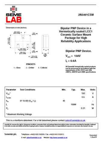
2N5401CSM Dimensions in mm (inches). Bipolar PNP Device in a 0.51 0.10 Hermetically sealed LCC1 (0.02 0.004) 0.31 rad. (0.012) Ceramic Surface Mount 3 Package for High Reliability Applications 21 1.91 0.10 (0.075 0.004) A 0.31 rad. Bipolar PNP Device. (0.012) 3.05 0.13 (0.12 0.005) 1.40 (0.055) 1.02 0.10 max. VCEO = 150V A = (0.04 0.00
2n5430x.pdf
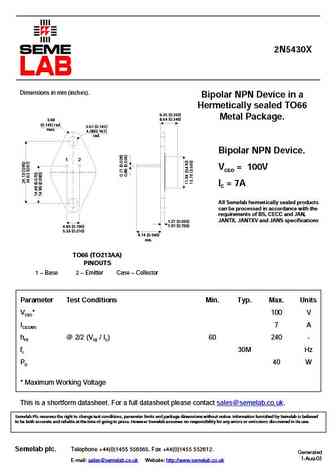
2N5430X Dimensions in mm (inches). Bipolar NPN Device in a Hermetically sealed TO66 6.35 (0.250) Metal Package. 8.64 (0.340) 3.68 (0.145) rad. 3.61 (0.142) max. 4.08(0.161) rad. Bipolar NPN Device. 1 2 VCEO = 100V IC = 7A All Semelab hermetically sealed products can be processed in accordance with the requirements of BS, CECC and JAN, JANTX, JANTXV and JANS spec
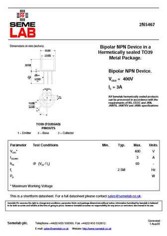
2n5468.pdf
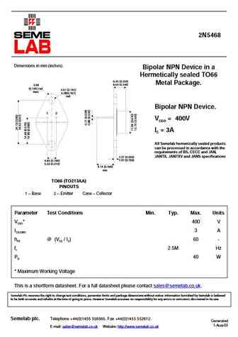
2N5468 Dimensions in mm (inches). Bipolar NPN Device in a Hermetically sealed TO66 6.35 (0.250) Metal Package. 8.64 (0.340) 3.68 (0.145) rad. 3.61 (0.142) max. 4.08(0.161) rad. Bipolar NPN Device. 1 2 VCEO = 400V IC = 3A All Semelab hermetically sealed products can be processed in accordance with the requirements of BS, CECC and JAN, JANTX, JANTXV and JANS speci
2n5428a.pdf
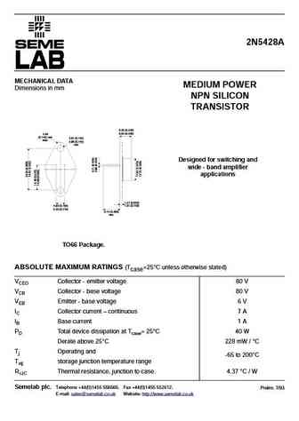
2N5428A MECHANICAL DATA MEDIUM POWER Dimensions in mm NPN SILICON TRANSISTOR 6.35 (0.250) 8.64 (0.340) 3.68 (0.145) rad. 3.61 (0.142) max. 3.86 (0.145) rad. Designed for switching and wide - band amplifier applications 1.27 (0.050) 4.83 (0.190) 1.91 (0.750) 5.33 (0.210) 9.14 (0.360) min. TO66 Package. ABSOLUTE MAXIMUM RATINGS (Tcase=25 C unless otherwise stated) VCEO Co
2n5407x.pdf
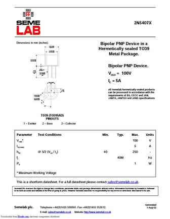
2N5407X Dimensions in mm (inches). Bipolar PNP Device in a 8.51 (0.34) 9.40 (0.37) Hermetically sealed TO39 7.75 (0.305) 8.51 (0.335) Metal Package. 6.10 (0.240) 6.60 (0.260) Bipolar PNP Device. 0.89 (0.035)max. 12.70 (0.500) min. 0.41 (0.016) 0.53 (0.021) VCEO = 100V dia. IC = 5A 5.08 (0.200) typ. 2.54 All Semelab hermetically sealed products 2 (0.100) 1 3
2n5414.pdf
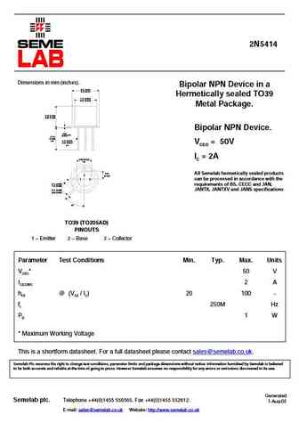
2N5414 Dimensions in mm (inches). Bipolar NPN Device in a 8.51 (0.34) 9.40 (0.37) Hermetically sealed TO39 7.75 (0.305) 8.51 (0.335) Metal Package. 6.10 (0.240) 6.60 (0.260) Bipolar NPN Device. 0.89 max. (0.035) 12.70 (0.500) min. 0.41 (0.016) 0.53 (0.021) VCEO = 50V dia. IC = 2A 5.08 (0.200) typ. 2.54 All Semelab hermetically sealed products 2 (0.100) 1 3
2n5469.pdf

2N5469 Dimensions in mm (inches). Bipolar NPN Device in a Hermetically sealed TO66 6.35 (0.250) Metal Package. 8.64 (0.340) 3.68 (0.145) rad. 3.61 (0.142) max. 4.08(0.161) rad. Bipolar NPN Device. 1 2 VCEO = 400V IC = 3A All Semelab hermetically sealed products can be processed in accordance with the requirements of BS, CECC and JAN, JANTX, JANTXV and JANS speci
2n5414cecc.pdf
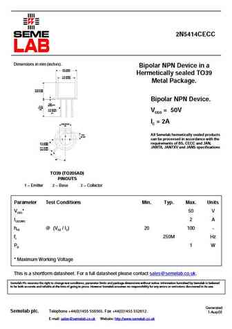
2N5414CECC Dimensions in mm (inches). Bipolar NPN Device in a 8.51 (0.34) 9.40 (0.37) Hermetically sealed TO39 7.75 (0.305) 8.51 (0.335) Metal Package. 6.10 (0.240) 6.60 (0.260) Bipolar NPN Device. 0.89 max. (0.035) 12.70 (0.500) min. 0.41 (0.016) 0.53 (0.021) VCEO = 50V dia. IC = 2A 5.08 (0.200) typ. 2.54 All Semelab hermetically sealed products 2 (0.100)
2n5404 2n5405 2n5406 2n5407.pdf
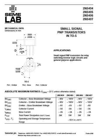
2N5404 2N5405 2N5406 2N5407 MECHANICAL DATA SMALL SIGNAL Dimensions in mm PNP TRANSISTORS 8.89 (0.35) 9.40 (0.37) IN TO-5 7.75 (0.305) 8.51 (0.335) 4.19 (0.165) 4.95 (0.195) 0.89 max. (0.035) 38.1 (1.500) APPLICATIONS min. 7.75 (0.305) 8.51 (0.335) dia. Small signal PNP transistors for relay 5.08 (0.200) switching resistor logic circuits and typ. general purpose appli
2n5401dcsm.pdf
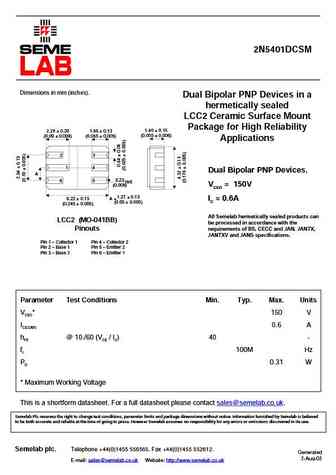
2N5401DCSM Dimensions in mm (inches). Dual Bipolar PNP Devices in a hermetically sealed LCC2 Ceramic Surface Mount Package for High Reliability 1.40 0.15 2.29 0.20 1.65 0.13 (0.055 0.006) (0.09 0.008) (0.065 0.005) Applications 2 3 1 4 Dual Bipolar PNP Devices. A 0.23 6 5 rad. (0.009) V = 150V CEO 6.22 0.13 A = 1.27 0.13 I = 0.6A C (0.
2n5467.pdf
2N5467 Dimensions in mm (inches). Bipolar NPN Device in a 8.51 (0.34) 9.40 (0.37) Hermetically sealed TO39 7.75 (0.305) 8.51 (0.335) Metal Package. 6.10 (0.240) 6.60 (0.260) Bipolar NPN Device. 0.89 max. (0.035) 12.70 (0.500) min. 0.41 (0.016) 0.53 (0.021) VCEO = 400V dia. IC = 3A 5.08 (0.200) typ. 2.54 All Semelab hermetically sealed products 2 (0.100) 1 3
2n5401.pdf
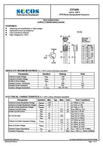
2N5401 -0.6 A, -160 V PNP Plastic Encapsulated Transistor Elektronische Bauelemente RoHS Compliant Product A suffix of -C specifies halogen & lead-free TO-92 FEATURES G H Switching and amplification in high voltage Applications such as telephony J Low current (max. 600mA) A D Millimeter REF. Min. Max. B High voltage (max. 160V) A 4.40 4.70 B 4.30
2n5400.pdf
2N5400 -0.6 A, -130 V PNP Plastic Encapsulated Transistor Elektronische Bauelemente RoHS Compliant Product A suffix of -C specifies halogen & lead-free FEATURES Switching and amplification in high voltage Applications such as telephony TO-92 Low current(max.600mA) High voltage(max.130V) G H Emitter Base Collector J A D Millimeter
2n5401.pdf
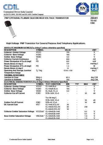
Continental Device India Limited An ISO/TS 16949, ISO 9001 and ISO 14001 Certified Company PNP EPITAXIAL PLANAR SILICON HIGH VOLTAGE TRANSISTOR 2N5401 TO-92 CBE C B E High Voltage PNP Transistor For General Purpose And Telephony Applications. ABSOLUTE MAXIMUM RATINGS(Ta=25deg C unless otherwise specified) DESCRIPTION SYMBOL VALUE UNIT Collector -Emitter Voltage VCEO 150 V Collector
2n5496.pdf
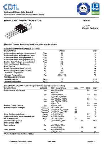
Continental Device India Limited An ISO/TS 16949, ISO 9001 and ISO 14001 Certified Company NPN PLASTIC POWER TRANSISTOR 2N5496 TO-220 Plastic Package Medium Power Switching and Amplifier Applications ABSOLUTE MAXIMUM RATINGS (Ta=25 C) DESCRIPTION VALUE UNIT Collector Base Voltage (Open emitter) VCBO 90 V Collector Emitter Voltage(open base) VCEO 70 V Collector Emitter Voltage(Vbe=1.5
2n5415 2n5416.pdf
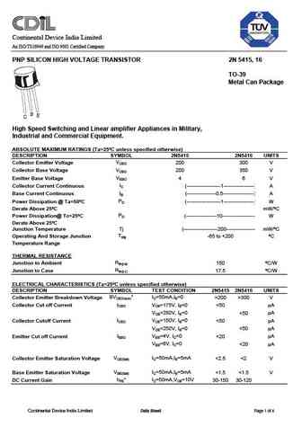
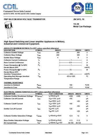
Continental Device India Limited An ISO/TS16949 and ISO 9001 Certified Company PNP SILICON HIGH VOLTAGE TRANSISTOR 2N 5415, 16 TO-39 Metal Can Package High Speed Switching and Linear amplifier Appliances in Military, Industrial and Commercial Equipment. ABSOLUTE MAXIMUM RATINGS (Ta=25 C unless specified otherwise) DESCRIPTION SYMBOL 2N5415 2N5416 UNITS VCEO Collector Emitter Voltage
2n5415 16.pdf
Continental Device India Limited An ISO/TS 16949, ISO 9001 and ISO 14001 Certified Company PNP SILICON HIGH VOLTAGE TRANSISTOR 2N 5415, 16 TO-39 Metal Can Package High Speed Switching and Linear amplifier Appliances in Military, Industrial and Commercial Equipment. ABSOLUTE MAXIMUM RATINGS (Ta=25 C unless specified otherwise) DESCRIPTION SYMBOL 2N5415 2N5416 UNITS VCEO Collector Emit
2n5400.pdf
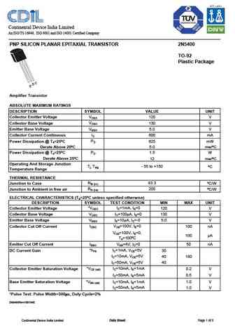
Continental Device India Limited An ISO/TS 16949, ISO 9001 and ISO 14001 Certified Company PNP SILICON PLANAR EPITAXIAL TRANSISTOR 2N5400 TO-92 Plastic Package C B E Amplifier Transistor ABSOLUTE MAXIMUM RATINGS DESCRIPTION SYMBOL VALUE UNIT Collector Emitter Voltage VCEO 120 V Collector Base Voltage VCBO 130 V Emitter Base Voltage VEBO 5.0 V Collector Current Continuous IC 600 mA
2n5401.pdf
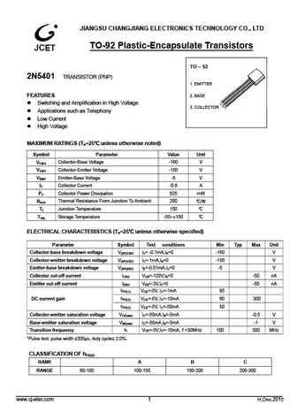
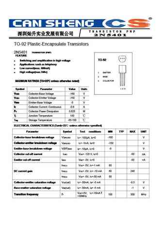
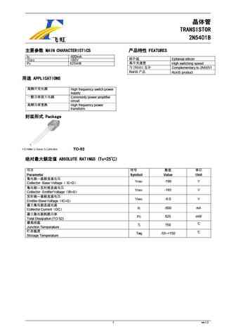
JIANGSU CHANGJIANG ELECTRONICS TECHNOLOGY CO., LTD TO-92 Plastic-Encapsulate Transistors TO 92 2N5401 TRANSISTOR (PNP) 1. EMITTER FEATURES 2. BASE Switching and Amplification in High Voltage 3. COLLECTOR Applications such as Telephony Low Current High Voltage MAXIMUM RATINGS (Ta=25 unless otherwise noted) Symbol Parameter Value Unit VCBO Collector-Base Volta
2n5498.pdf
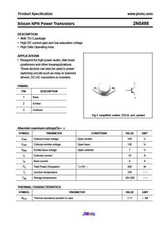
Product Specification www.jmnic.com Silicon NPN Power Transistors 2N5498 DESCRIPTION With TO-3 package High DC current gain and low saturation voltage High Safe Operating Area APPLICATIONS Designed for high power audio, disk head positioners and other linearapplications. These devices can also be used in power switching circuits such as relay or solenoid drivers,
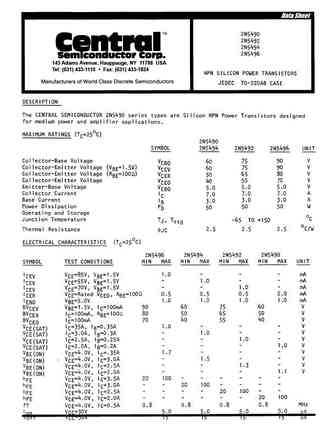
2n5490 2n5492 2n5494 2n5496.pdf
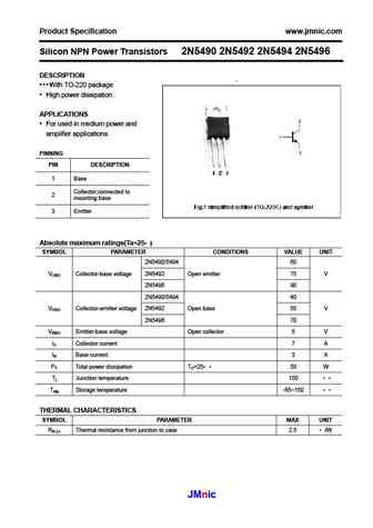
Product Specification www.jmnic.com Silicon NPN Power Transistors 2N5490 2N5492 2N5494 2N5496 DESCRIPTION With TO-220 package High power dissipation APPLICATIONS For used in medium power and amplifier applications PINNING PIN DESCRIPTION 1 Base Collector;connected to 2 mounting base 3 Emitter Absolute maximum ratings(Ta=25 ) SYMBOL PARAMETER CONDITIONS
2n5401.pdf
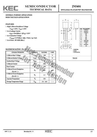
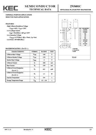
SEMICONDUCTOR 2N5401 TECHNICAL DATA EPITAXIAL PLANAR PNP TRANSISTOR GENERAL PURPOSE APPLICATION. HIGH VOLTAGE APPLICATION. B C FEATURES High Collector Breakdwon Voltage N DIM MILLIMETERS VCBO=-160V, VCEO=-150V A 4.70 MAX E K Low Leakage Current. B 4.80 MAX G C 3.70 MAX D ICBO=-50nA(Max.) @VCB=-120V D 0.45 E 1.00 Low Saturation Voltage F 1.27 G 0.85 VCE(sat)=-
2n5401c.pdf
SEMICONDUCTOR 2N5401C TECHNICAL DATA EPITAXIAL PLANAR PNP TRANSISTOR GENERAL PURPOSE APPLICATION. HIGH VOLTAGE APPLICATION. B C FEATURES High Collector Breakdwon Voltage N DIM MILLIMETERS VCBO=-160V, VCEO=-150V A 4.70 MAX E K Low Leakage Current. B 4.80 MAX G C 3.70 MAX D ICBO=-50nA(Max.) @VCB=-120V D 0.45 E 1.00 Low Saturation Voltage F 1.27 G 0.85 VCE(sat)=-0.5V(
2n5400s.pdf
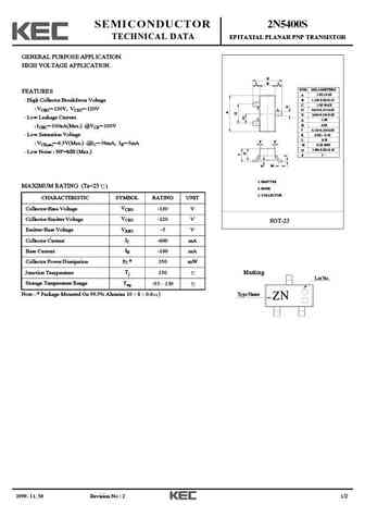
SEMICONDUCTOR 2N5400S TECHNICAL DATA EPITAXIAL PLANAR PNP TRANSISTOR GENERAL PURPOSE APPLICATION. HIGH VOLTAGE APPLICATION. E L B L DIM MILLIMETERS FEATURES _ + 2.93 0.20 A B 1.30+0.20/-0.15 High Collector Breakdwon Voltage C 1.30 MAX 2 VCBO=-130V, VCEO=-120V 3 D 0.45+0.15/-0.05 E 2.40+0.30/-0.20 Low Leakage Current. 1 G 1.90 H 0.95 ICBO=-100nA(Max.) @VCB=-100V J 0.
2n5400.pdf

SEMICONDUCTOR 2N5400 TECHNICAL DATA EPITAXIAL PLANAR PNP TRANSISTOR GENERAL PURPOSE APPLICATION. HIGH VOLTAGE APPLICATION. B C FEATURES High Collector Breakdwon Voltage N DIM MILLIMETERS VCBO=-130V, VCEO=-120V A 4.70 MAX E K Low Leakage Current. B 4.80 MAX G C 3.70 MAX D ICBO=-100nA(Max.) @VCB=-100V D 0.45 E 1.00 Low Saturation Voltage F 1.27 G 0.85 VCE(sat)=-0.5V(
2n5401s.pdf
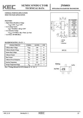
SEMICONDUCTOR 2N5401S TECHNICAL DATA EPITAXIAL PLANAR PNP TRANSISTOR GENERAL PURPOSE APPLICATION. HIGH VOLTAGE APPLICATION. E L B L DIM MILLIMETERS _ FEATURES A 2.93 0.20 + B 1.30+0.20/-0.15 High Collector Breakdwon Voltage C 1.30 MAX 2 3 D 0.40+0.15/-0.05 VCBO=-160V, VCEO=-150V E 2.40+0.30/-0.20 1 Low Leakage Current. G 1.90 H 0.95 ICBO=-50nA(Max.) @VCB=-120V J 0.
2n5401.pdf
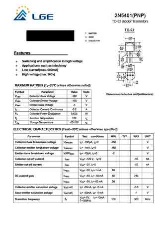
2N5401(PNP) TO-92 Bipolar Transistors TO-92 1. EMITTER 2. BASE 3. COLLECTOR Features Switching and amplification in high voltage Applications such as telephony Low current(max. 600mA) High voltage(max.160v) MAXIMUM RATINGS (TA=25 unless otherwise noted) Symbol Parameter Value Units Dimensions in inches and (millimeters) VCBO Collector-Base Voltage -160 V
2n5400.pdf

2N5400(PNP) TO-92 Bipolar Transistors TO-92 1. EMITTER 2. BASE 3. COLLECTOR Features Switching and amplification in high voltage Applications such as telephony Low current(max. 600mA) High voltage(max.130v) MAXIMUM RATINGS (TA=25 unless otherwise noted) Dimensions in inches and (millimeters) Symbol Parameter Value Units VCBO Collector-Base Voltage -130 V
2n5401.pdf
2N5401 PNP Transistors TO-92 1 1. EMITTER 2 3 2. BASE 3. COLLECTOR ABSOLUTE MAXIMUM RATINGS (Ta=25 C) Rating Symbol 2N5401 Unit Collector-Emitter Voltage V CEO -150 Vdc Collector-Base Voltage VCBO -160 Vdc Emitter-Base VOltage VEBO -5.0 Vdc Collector Current IC 600 mAdc Total Device Dissipation T =25 C PD W 0.625 A Junction Temperature T 150 j C Storage, Temperature Tstg
h2n5401.pdf
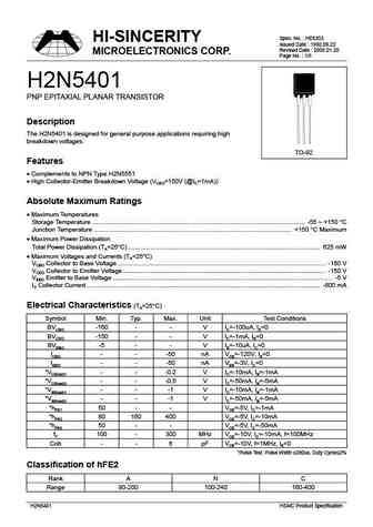
Spec. No. HE6203 HI-SINCERITY Issued Date 1992.09.22 Revised Date 2005.01.20 MICROELECTRONICS CORP. Page No. 1/5 H2N5401 PNP EPITAXIAL PLANAR TRANSISTOR Description The H2N5401 is designed for general purpose applications requiring high breakdown voltages. TO-92 Features Complements to NPN Type H2N5551 High Collector-Emitter Breakdown Voltage (VCEO=150V (@IC=1mA))
2n5401.pdf
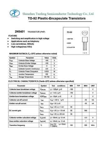
Shenzhen Tuofeng Semiconductor Technology Co., Ltd TO-92 Plastic-Encapsulate Transistors 2N5401 TRANSISTOR (PNP) TO-92 FEATURE Switching and amplification in high voltage 1.EMITTER Applications such as telephony 2.BASE Low current(max. 600mA) High voltage(max.160v) 3.COLLECTOR 1 2 3 MAXIMUM RATINGS (TA=25 unless otherwise noted) Symbol Parameter Value
2n5401.pdf
TO-92 Plastic-Encapsulate Transistors TRANSISTOR (PNP) TRANSISTOR (PNP) TRANSISTOR (PNP) 2N5401 TRANSISTOR (PNP) FEATURE FEATURE FEATURE FEATURE TO-92 TO-92 TO-92 TO-92 Switching and amplification in high voltage Switching and amplification in high voltage Switching and amplification in high voltage Switching and amplification in high voltage Applications su
2n5401.pdf
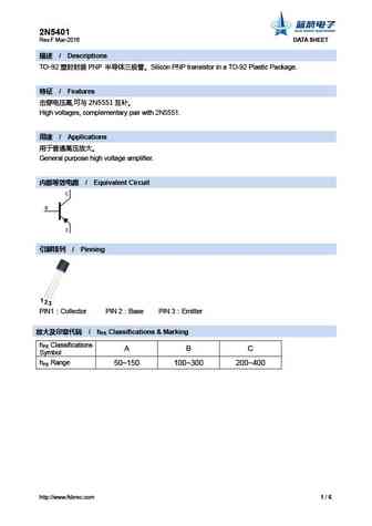
2N5401 Rev.F Mar-2016 DATA SHEET / Descriptions TO-92 PNP Silicon PNP transistor in a TO-92 Plastic Package. / Features , 2N5551 High voltages, complementary pair with 2N5551. / Applications General purpose high voltage amplifier. / Equivalent
2n5400 2n5401.pdf
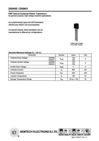
2N5400 / 2N5401 PNP Silicon Epitaxial Planar Transistors for general purpose, high voltage amplifier applications. As complementary types the NPN transistors 2N5550 and 2N5551 are recommended. On special request, these transistors can be manufactured in different pin configurations. 1. Emitter 2. Base 3. Collector TO-92 Plastic Package O Absolute Maximum Ratings (Ta = 25 C)
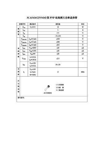
3ca5416 2n5416.pdf
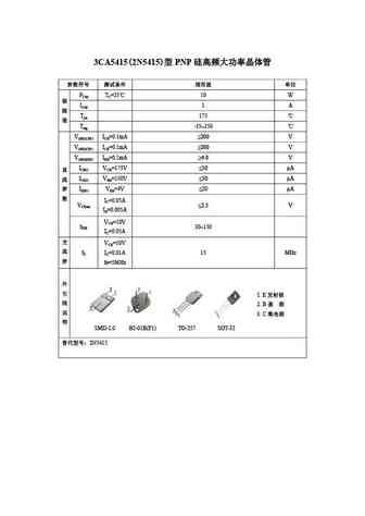
3CA5416(2N5416) PNP PCM TC=25 10 W ICM 1 A Tjm 175 Tstg -55 150 V(BR)CBO ICB=0.1mA 350 V V(BR)CEO ICE=0.1mA 300 V V(BR)EBO IEB=0.1mA 6.0 V ICBO VCB=280V 50 A ICEO VEB=150V 50 A IEBO VEB=6V 20 A IC=0.05A VCEsat 2.5 V IB=0.
3ca5415 2n5415.pdf
3CA5415(2N5415) PNP PCM TC=25 10 W ICM 1 A Tjm 175 Tstg -55 150 V(BR)CBO ICB=0.1mA 200 V V(BR)CEO ICE=0.1mA 200 V V(BR)EBO IEB=0.1mA 4.0 V ICBO VCB=175V 50 A ICEO VEB=150V 50 A IEBO VEB=4V 20 A IC=0.05A VCEsat 2.5 V IB=0.
2n5401.pdf
SEMICONDUCTOR 2N5401 TECHNICAL DATA 2N5401 TRANSISTOR (PNP) B C FEATURE Switching and Amplification in High Voltage Applications such as Telephony DIM MILLIMETERS Low Current(Max. 600mA) A 4.70 MAX E B 4.80 MAX G High Voltage(Max.160v) C 3.70 MAX D D 0.55 MAX E 1.00 F 1.27 G 0.85 H 0.45 _ MAXIMUM RATINGS (Ta=25 unless otherwise noted) H J 14.00 0.50 + L 2
2n5401s.pdf
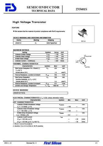
SEMICONDUCTOR 2N5401S TECHNICAL DATA High Voltage Transistor FEATURE 3 We declare that the material of product compliance with RoHS requirements. 2 1 DEVICE MARKING AND ORDERING INFORMATION Device Marking Shipping SOT 23 2N5401S 2L 3000/Tape&Reel MAXIMUM RATINGS Rating Symbol Value Unit Collector Emitter Voltage V 150 Vdc CEO 3 COLLECTOR Collector Base Voltage V CB
2n5401.pdf
2N5401 TO-92 Plastic-Encapsulate Transistors FEATURES TO 92 Switching and Amplification in High Voltage Applications such as Telephony 1. EMITTER Low Current High Voltage 2. BASE PNP Transistors 3. COLLECTOR MAXIMUM RATINGS (Ta=25 unless otherwise noted) Symbol Parameter Value Unit VCBO Collector-Base Voltage -160 V VCEO Collector-Emitter Voltage -150 V VEB
2n5419 2n5420 2n5550 2n5551 2n5830 2n5831 2n5832 2n5998 2n5999 2n6008 2n6009 2n6076 2n6426 2n6427.pdf

2n5306 2n5306a 2n5307 2n5308 2n5308a 2n5309 2n5310 2n5354 2n5355 2n5356 2n5365 2n5366 2n5367 2n5400 2n5401 2n5418.pdf
2n5401.pdf
2N5401 2N5401 TRANSISTOR (PNP) B C FEATURE Switching and Amplification in High Voltage Applications such as Telephony DIM MILLIMETERS Low Current(Max. 600mA) A 4.70 MAX E B 4.80 MAX G High Voltage(Max.160v) C 3.70 MAX D D 0.55 MAX E 1.00 F 1.27 G 0.85 H 0.45 _ MAXIMUM RATINGS (Ta=25 unless otherwise noted) H J 14.00 0.50 + L 2.30 F F M 0.51 MAX Symbol Pa
2n5401u.pdf
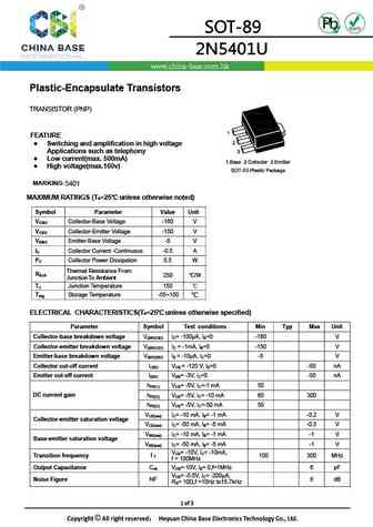
Plastic-Encapsulate Transistors TRANSISTOR (PNP) FEATURE Switching and amplification in high voltage Applications such as telephony Low current(max. 500mA) High voltage(max.160v) MARKING 5401 MAXIMUM RATINGS (Ta=25 unless otherwise noted) Symbol Parameter Value Unit VCBO Collector-Base Voltage -160 V VCEO Collector-Emitter Voltage -150 V VEBO Emitter-Base Volta
2n5430.pdf
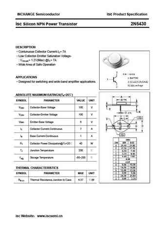
INCHANGE Semiconductor isc Product Specification isc Silicon NPN Power Transistor 2N5430 DESCRIPTION Contunuous Collector Current-IC= 7A Low Collector-Emitter Saturation Voltage- VCE(sat)= 1.2V(Max) @IC= 7A Wide Area of Safe Operation APPLICATIONS Designed for switching and wide-band amplifier applications. ABSOLUTE MAXIMUM RATINGS(Ta=25 ) SYMBOL PARAMETER VALUE
2n5468.pdf
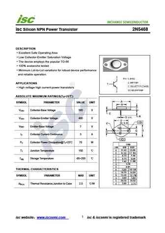
isc Silicon NPN Power Transistor 2N5468 DESCRIPTION Excellent Safe Operating Area Low Collector-Emitter Saturation Voltage The device employs the popular TO-66 100% avalanche tested Minimum Lot-to-Lot variations for robust device performance and reliable operation. APPLICATIONS High voltage high current power transistors ABSOLUTE MAXIMUM RATINGS(T =25 ) a SYMBOL PARAME
2n5429.pdf

INCHANGE Semiconductor isc Product Specification isc Silicon NPN Power Transistor 2N5429 DESCRIPTION Contunuous Collector Current-IC= 7A Low Collector-Emitter Saturation Voltage- VCE(sat)= 1.2V(Max) @IC= 7A Wide Area of Safe Operation APPLICATIONS Designed for switching and wide-band amplifier applications. ABSOLUTE MAXIMUM RATINGS(Ta=25 ) SYMBOL PARAMETER VALUE
2n5490.pdf
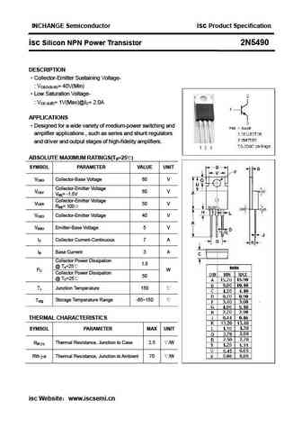
INCHANGE Semiconductor isc Product Specification isc Silicon NPN Power Transistor 2N5490 DESCRIPTION Collector-Emitter Sustaining Voltage- VCEO(SUS)= 40V(Min) Low Saturation Voltage- VCE (sat)= 1V(Max)@IC= 2.0A APPLICATIONS Designed for a wide variety of medium-power switching and amplifier applications , such as series and shunt regulators and driver and output
2n5492.pdf

INCHANGE Semiconductor isc Product Specification isc Silicon NPN Power Transistor 2N5492 DESCRIPTION Collector-Emitter Sustaining Voltage- VCEO(SUS)= 55V(Min) Low Saturation Voltage- VCE (sat)= 1V(Max)@IC= 2.5A APPLICATIONS Designed for a wide variety of medium-power switching and amplifier applications , such as series and shunt regulators and driver and output
2n5469.pdf

isc Silicon NPN Power Transistor 2N5469 DESCRIPTION Excellent Safe Operating Area Low Collector-Emitter Saturation Voltage The device employs the popular TO-66 100% avalanche tested Minimum Lot-to-Lot variations for robust device performance and reliable operation. APPLICATIONS High voltage high current power transistors ABSOLUTE MAXIMUM RATINGS(T =25 ) a SYMBOL PARAME
2n5493.pdf

INCHANGE Semiconductor isc Product Specification isc Silicon NPN Power Transistor 2N5493 DESCRIPTION Collector-Emitter Sustaining Voltage- VCEO(SUS)= 55V(Min) Low Saturation Voltage- VCE (sat)= 1V(Max)@IC= 2.5A APPLICATIONS Designed for a wide variety of medium-power switching and amplifier applications , such as series and shunt regulators and driver and output s
2n5468 2n5469.pdf
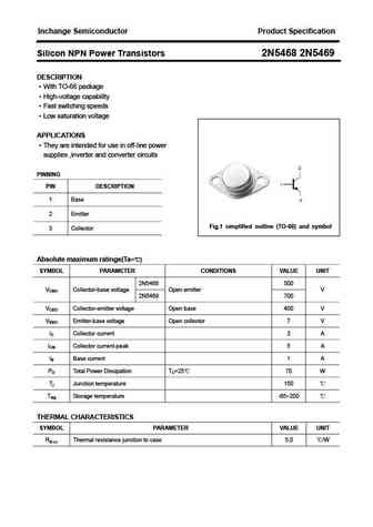
Inchange Semiconductor Product Specification Silicon NPN Power Transistors 2N5468 2N5469 DESCRIPTION With TO-66 package High-voltage capability Fast switching speeds Low saturation voltage APPLICATIONS They are intended for use in off-line power supplies ,inverter and converter circuits PINNING PIN DESCRIPTION 1 Base 2 Emitter Fig.1 simplified outline (TO-66)
2n5495.pdf
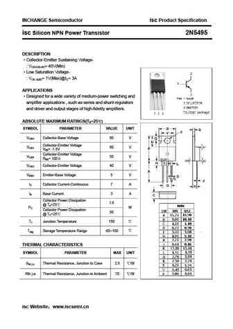
INCHANGE Semiconductor isc Product Specification isc Silicon NPN Power Transistor 2N5495 DESCRIPTION Collector-Emitter Sustaining Voltage- VCEO(SUS)= 40V(Min) Low Saturation Voltage- VCE (sat)= 1V(Max)@IC= 3A APPLICATIONS Designed for a wide variety of medium-power switching and amplifier applications , such as series and shunt regulators and driver and output sta
2n5498.pdf
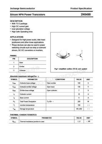
Inchange Semiconductor Product Specification Silicon NPN Power Transistors 2N5498 DESCRIPTION With TO-3 package High DC current gain Low saturation voltage High Safe Operating Area APPLICATIONS Designed for high power audio, disk head positioners and other linear applications. These devices can also be used in power switching circuits such as relay or solenoid
2n5427.pdf

INCHANGE Semiconductor isc Product Specification isc Silicon NPN Power Transistor 2N5427 DESCRIPTION Contunuous Collector Current-IC= 7A Low Collector-Emitter Saturation Voltage- VCE(sat)= 1.2V(Max) @IC= 7A Wide Area of Safe Operation APPLICATIONS Designed for switching and wide-band amplifier applications. ABSOLUTE MAXIMUM RATINGS(Ta=25 ) SYMBOL PARAMETER VALUE
2n5491.pdf
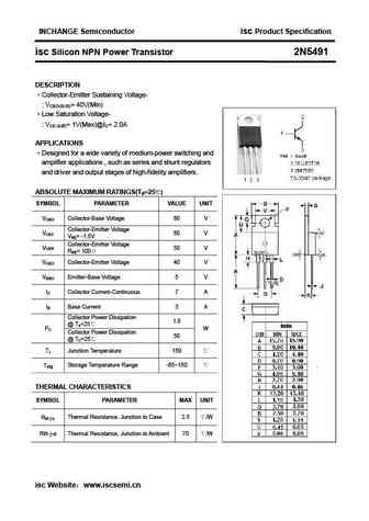
INCHANGE Semiconductor isc Product Specification isc Silicon NPN Power Transistor 2N5491 DESCRIPTION Collector-Emitter Sustaining Voltage- VCEO(SUS)= 40V(Min) Low Saturation Voltage- VCE (sat)= 1V(Max)@IC= 2.0A APPLICATIONS Designed for a wide variety of medium-power switching and amplifier applications , such as series and shunt regulators and driver and output
2n5466 2n5467.pdf
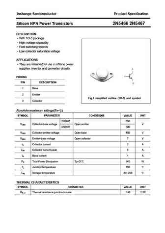
Inchange Semiconductor Product Specification Silicon NPN Power Transistors 2N5466 2N5467 DESCRIPTION With TO-3 package High-voltage capability Fast switching speeds Low collector saturation voltage APPLICATIONS They are intended for use in off-line power supplies ,inverter and converter circuits PINNING PIN DESCRIPTION 1 Base 2 Emitter Fig.1 simplified outlin
2n5467.pdf
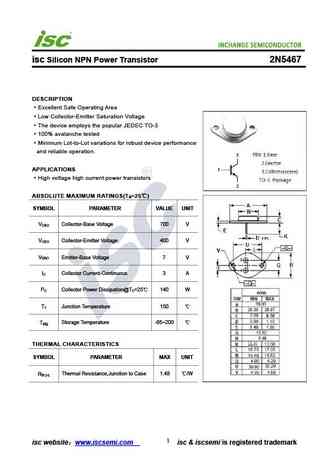
isc Silicon NPN Power Transistor 2N5467 DESCRIPTION Excellent Safe Operating Area Low Collector-Emitter Saturation Voltage The device employs the popular JEDEC TO-3 100% avalanche tested Minimum Lot-to-Lot variations for robust device performance and reliable operation. APPLICATIONS High voltage high current power transistors ABSOLUTE MAXIMUM RATINGS(T =25 ) a SYMBOL P
2n5466.pdf
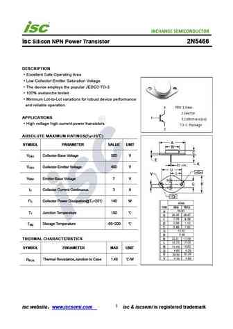
isc Silicon NPN Power Transistor 2N5466 DESCRIPTION Excellent Safe Operating Area Low Collector-Emitter Saturation Voltage The device employs the popular JEDEC TO-3 100% avalanche tested Minimum Lot-to-Lot variations for robust device performance and reliable operation. APPLICATIONS High voltage high current power transistors ABSOLUTE MAXIMUM RATINGS(T =25 ) a SYMBOL P
2n5428.pdf

INCHANGE Semiconductor isc Product Specification isc Silicon NPN Power Transistor 2N5428 DESCRIPTION Contunuous Collector Current-IC= 7A Low Collector-Emitter Saturation Voltage- VCE(sat)= 1.2V(Max) @IC= 7A Wide Area of Safe Operation APPLICATIONS Designed for switching and wide-band amplifier applications. ABSOLUTE MAXIMUM RATINGS(Ta=25 ) SYMBOL PARAMETER VALUE
2n5490 2n5492 2n5494 2n5496.pdf
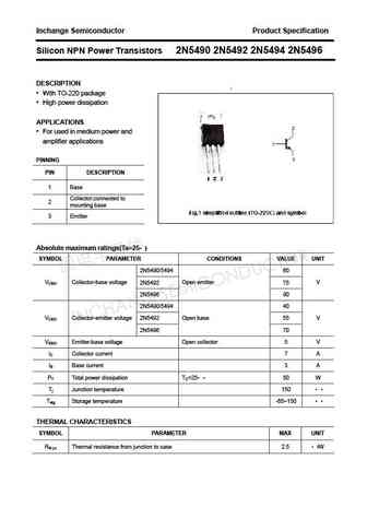
Inchange Semiconductor Product Specification Silicon NPN Power Transistors 2N5490 2N5492 2N5494 2N5496 DESCRIPTION With TO-220 package High power dissipation APPLICATIONS For used in medium power and amplifier applications PINNING PIN DESCRIPTION 1 Base Collector;connected to 2 mounting base 3 Emitter Absolute maximum ratings(Ta=25 ) SYMBOL PARAMETER CONDI
2n5497.pdf

INCHANGE Semiconductor isc Product Specification isc Silicon NPN Power Transistor 2N5497 DESCRIPTION Collector-Emitter Sustaining Voltage- VCEO(SUS)= 70V(Min) Low Saturation Voltage- VCE (sat)= 1V(Max)@IC= 3.5A APPLICATIONS Designed for a wide variety of medium-power switching and amplifier applications , such as series and shunt regulators and driver and output
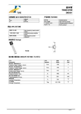
Otros transistores... 2N5388, 2N5389, 2N538A, 2N538M, 2N539, 2N5390, 2N5399, 2N539A, 2SD669A, 2N540, 2N5400, 2N5401, 2N5404, 2N5405, 2N5406, 2N5407, 2N5408
Parámetros del transistor bipolar y su interrelación.
🌐 : EN ES РУ

Liste
Recientemente añadidas las descripciónes de los transistores:
BJT: ZDT6705 | GA1L4Z | GA1A4M | SBT42 | 2SA200-Y | 2SA200-O | 2SD882-Q | 2SD882-P | 2SD882-E | 2SC945-L | 2SC945-H | 2SC4226-R23 | 2SC3357-F | 2SC3357-E | 2SC3356-R26 | 2SC3356-R24 | 2SC3356-R23 | 2SB772-Q | 2SB772-P | 2SB772-E | 2SA1015-L
Popular searches
irf3205 datasheet | irf5210 | mj15024 | 2n2219 | tip42c | 2sc2240 | bc547 transistor equivalent | 2sa1943