2N5559 Equivalente. Reemplazo. Hoja de especificaciones. Principales características
Número de Parte: 2N5559
Material: Si
Polaridad de transistor: NPN
ESPECIFICACIONES MÁXIMAS
Disipación total del dispositivo (Pc): 100 W
Tensión colector-base (Vcb): 150 V
Tensión colector-emisor (Vce): 120 V
Tensión emisor-base (Veb): 7 V
Corriente del colector DC máxima (Ic): 10 A
Temperatura operativa máxima (Tj): 200 °C
CARACTERÍSTICAS ELÉCTRICAS
Transición de frecuencia (fT): 0.8 MHz
Capacitancia de salida (Cc): 600 pF
Ganancia de corriente contínua (hFE): 12
Encapsulados: TO3
Búsqueda de reemplazo de 2N5559
- Selecciónⓘ de transistores por parámetros
2N5559 datasheet
2n5559.pdf
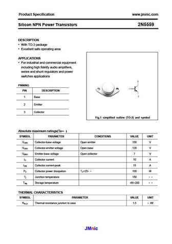
Product Specification www.jmnic.com Silicon NPN Power Transistors 2N5559 DESCRIPTION With TO-3 package Excellent safe operating area APPLICATIONS For industrial and commercial equipment including high fidelity audio amplifiers, series and shunt regulators and power switches applications PINNING PIN DESCRIPTION 1 Base 2 Emitter 3 Collector Fig.1 simplified outlin
2n5559.pdf
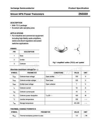
Inchange Semiconductor Product Specification Silicon NPN Power Transistors 2N5559 DESCRIPTION With TO-3 package Excellent safe operating area APPLICATIONS For industrial and commercial equipment including high fidelity audio amplifiers, series and shunt regulators and power switches applications PINNING PIN DESCRIPTION 1 Base 2 Emitter Fig.1 simplified outline (T
2n5550 2n5551.pdf
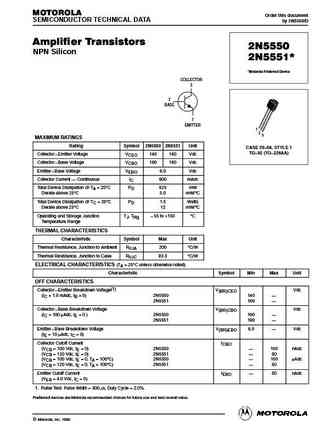
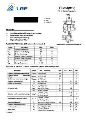
MOTOROLA Order this document SEMICONDUCTOR TECHNICAL DATA by 2N5550/D Amplifier Transistors 2N5550 NPN Silicon * 2N5551 *Motorola Preferred Device COLLECTOR 3 2 BASE 1 EMITTER 1 2 3 MAXIMUM RATINGS Rating Symbol 2N5550 2N5551 Unit CASE 29 04, STYLE 1 TO 92 (TO 226AA) Collector Emitter Voltage VCEO 140 160 Vdc Collector Base Voltage VCBO 160 180 Vdc Emitter B
2n5555 2n5555rev0x.pdf
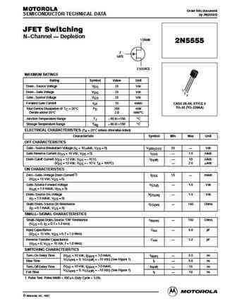
MOTOROLA Order this document SEMICONDUCTOR TECHNICAL DATA by 2N5555/D JFET Switching N Channel Depletion 1 DRAIN 2N5555 3 GATE 2 SOURCE MAXIMUM RATINGS Rating Symbol Value Unit Drain Source Voltage VDS 25 Vdc 1 Drain Gate Voltage VDG 25 Vdc 2 3 Gate Source Voltage VGS 25 Vdc Forward Gate Current IGF 10 mAdc CASE 29 04, STYLE 5 TO 92 (TO 226AA) Total Devic
2n5550 2n5551 2.pdf
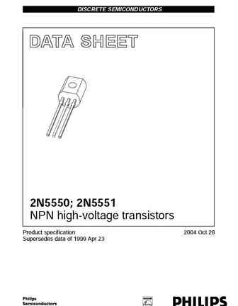
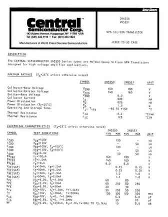
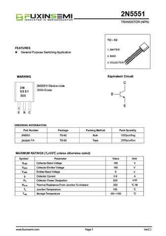
DISCRETE SEMICONDUCTORS DATA SHEET book, halfpage M3D186 2N5550; 2N5551 NPN high-voltage transistors Product specification 2004 Oct 28 Supersedes data of 1999 Apr 23 Philips Semiconductors Product specification NPN high-voltage transistors 2N5550; 2N5551 FEATURES PINNING Low current (max. 300 mA) PIN DESCRIPTION High voltage (max. 160 V). 1 collector 2 base APPLICATIONS
2n5551hr.pdf
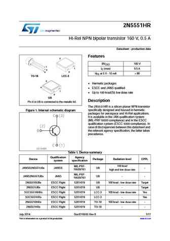
2N5551HR Hi-Rel NPN bipolar transistor 160 V, 0.5 A Datasheet - production data Features 3 BVCEO 160 V 1 1 IC (max) 0.5 A 2 2 3 HFE at 5 V - 10 mA > 80 TO-18 LCC-3 3 Hermetic packages 4 ESCC and JANS qualified 1 Up to 100 krad(Si) low dose rate 2 UB Description Pin 4 in UB is connected to the metallic lid. The 2N5551HR is a silicon planar NPN transistor spe
2n5551 mmbt5551.pdf
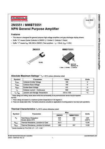
June 2009 2N5551 / MMBT5551 NPN General Purpose Amplifier Features This device is designed for general purpose high voltage amplifiers and gas discharge display drivers. Suffix -C means Center Collector in 2N5551 (1. Emitter 2. Collector 3. Base) Suffix -Y means hFE 180 240 in 2N5551 (Test condition IC = 10mA, VCE = 5.0V) 2N5551 MMBT5551 3 2 TO-92 SOT-23
2n5550.pdf
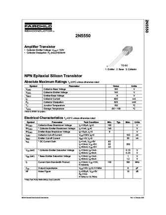
AmpIifier Transistor Collector-Emitter Voltage VCEO= 140V Collector Dissipation PC (max)=625mW TO-92 1. Emitter 2. Base 3. Collector NPN EpitaxiaI SiIicon Transistor AbsoIute Maximum Ratings Ta=25 C unless otherwise noted SymboI Parameter VaIue Units VCBO Collector-Base Voltage 160 V VCEO Collector-Emitter Voltage 140 V VEBO Emitter-Base Voltage 6 V IC
2n5551.pdf
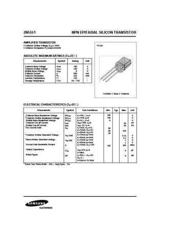
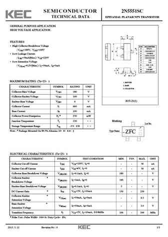
2N5551 NPN EPITAXIAL SILICON TRANSISTOR AMPLIFIER TRANSISTOR Collector-Emitter Voltage VCEO= 160V TO-92 Collector Dissipation PC (max)=625mW ABSOLUTE MAXIMUM RATINGS (T =25 ) A Characteristic Symbol Rating Unit Collector-Base Voltage VCBO 180 V Collector-Emitter Voltage VCEO 160 V Emitter-Base Voltage VEBO 6 V Collector Current IC 600 mA Collector Dissipation PC 625 mW Ju
2n5550 2n5551.pdf
145 Adams Avenue, Hauppauge, NY 11788 USA Tel (631) 435-1110 Fax (631) 435-1824
2n5551 to-92.pdf
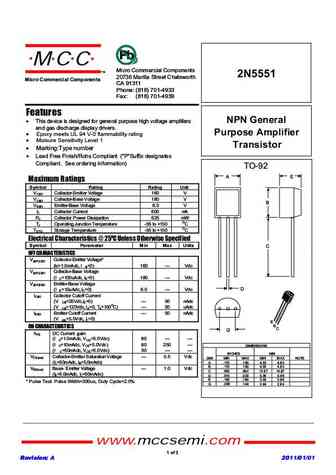
MCC Micro Commercial Components TM 2N5551 20736 Marilla Street Chatsworth Micro Commercial Components CA 91311 Phone (818) 701-4933 Fax (818) 701-4939 Features This device is designed for general purpose high voltage amplifiers NPN General and gas discharge display drivers. Purpose Amplifier Epoxy meets UL 94 V-0 flammability rating Moisure Sensitivity Level 1 Tr
2n5550 2n5551.pdf

2N5550, 2N5551 Preferred Device Amplifier Transistors NPN Silicon Features These are Pb-Free Devices* http //onsemi.com COLLECTOR 3 MAXIMUM RATINGS 2 Rating Symbol Value Unit BASE Collector - Emitter Voltage VCEO Vdc 2N5550 140 1 2N5551 160 EMITTER Collector - Base Voltage VCBO Vdc 2N5550 160 2N5551 180 Emitter - Base Voltage VEBO 6.0 Vdc TO-92 CASE 29 Collector Curr
2n5551ta 2n5551tfr 2n5551tf 2n5551bu mmbt5551.pdf
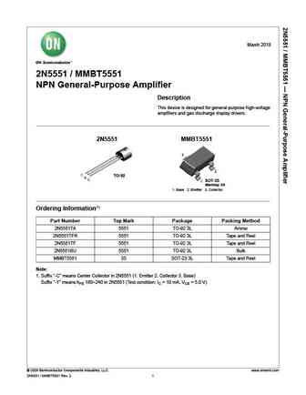
March March 20188 2N5551 / MMBT5551 NPN General-Purpose Amplifier Description This device is designed for general-purpose high-voltage amplifiers and gas discharge display drivers. 2N5551 MMBT5551 3 2 TO-92 SOT-23 1 Marking 3S 1. Base 2. Emitter 3. Collector Ordering Information(1) Part Number Top Mark Package Packing Method 2N5551TA 5551 TO-92 3L Ammo 2N5551TFR 5551 TO-92 3L
2n5550g.pdf
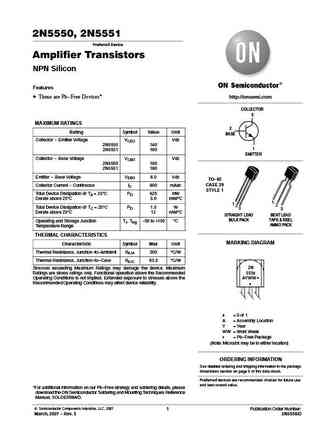
2N5550, 2N5551 Preferred Device Amplifier Transistors NPN Silicon Features These are Pb-Free Devices* http //onsemi.com COLLECTOR 3 MAXIMUM RATINGS 2 Rating Symbol Value Unit BASE Collector - Emitter Voltage VCEO Vdc 2N5550 140 1 2N5551 160 EMITTER Collector - Base Voltage VCBO Vdc 2N5550 160 2N5551 180 Emitter - Base Voltage VEBO 6.0 Vdc TO-92 CASE 29 Collector Curr
2n5551 mmbt5551.pdf

Is Now Part of To learn more about ON Semiconductor, please visit our website at www.onsemi.com Please note As part of the Fairchild Semiconductor integration, some of the Fairchild orderable part numbers will need to change in order to meet ON Semiconductor s system requirements. Since the ON Semiconductor product management systems do not have the ability to manage part nomenclatur
2n5550.pdf

Is Now Part of To learn more about ON Semiconductor, please visit our website at www.onsemi.com Please note As part of the Fairchild Semiconductor integration, some of the Fairchild orderable part numbers will need to change in order to meet ON Semiconductor s system requirements. Since the ON Semiconductor product management systems do not have the ability to manage part nomenclatur

2n5551.pdf
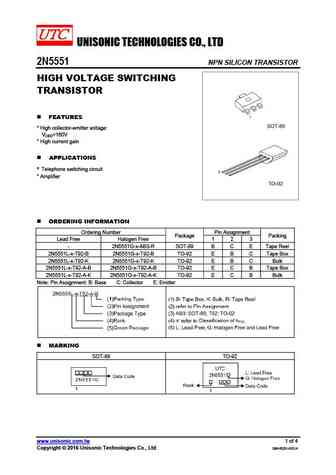
UNISONIC TECHNOLOGIES CO., LTD 2N5551 NPN SILICON TRANSISTOR HIGH VOLTAGE SWITCHING TRANSISTOR FEATURES * High collector-emitter voltage VCEO=160V * High current gain APPLICATIONS * Telephone switching circuit * Amplifier ORDERING INFORMATION Ordering Number Pin Assignment Package Packing Lead Free Halogen Free 1 2 3 - 2N5551G-x-AB3-R SOT-89 B C E Tape
2n5551g.pdf
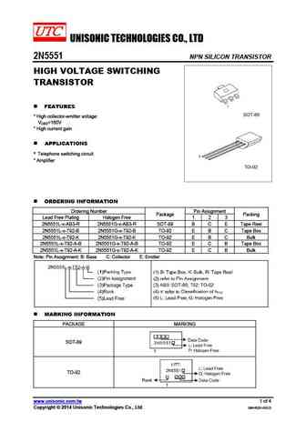
UNISONIC TECHNOLOGIES CO., LTD 2N5551 NPN SILICON TRANSISTOR HIGH VOLTAGE SWITCHING TRANSISTOR FEATURES * High collector-emitter voltage VCEO=160V * High current gain APPLICATIONS * Telephone switching circuit * Amplifier ORDERING INFORMATION Ordering Number Pin Assignment Package Packing Lead Free Plating Halogen Free 1 2 3 2N5551L-x-AB3-R 2N5551G-x-
2n5551.pdf
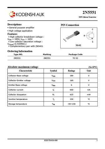
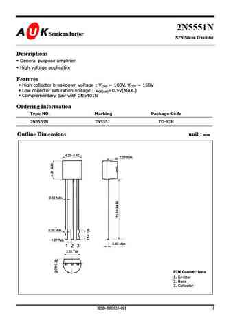
2N5551 NPN Silicon Transistor Descriptions PIN Connection General purpose amplifier C High voltage application Features B High collector breakdown voltage VCBO = 180V, VCEO = 160V Low collector saturation voltage E VCE(sat)=0.5V(MAX.) TO-92 Complementary pair with 2N5401 Ordering Information Type NO. Marking Package Code 2N5551 2N5551
2n5551n.pdf
2N5551N Semiconductor Semiconductor NPN Silicon Transistor Descriptions General purpose amplifier High voltage application Features High collector breakdown voltage VCBO = 180V, VCEO = 160V Low collector saturation voltage VCE(sat)=0.5V(MAX.) Complementary pair with 2N5401N Ordering Information Type NO. Marking Package Code 2N5551N 2N5551 TO-9
2n5551cn.pdf
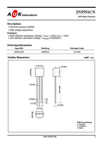
2N5551CN Semiconductor Semiconductor NPN Silicon Transistor Descriptions General purpose amplifier High voltage application Features High collector breakdown voltage VCBO = 180V, VCEO = 160V Low collector saturation voltage VCE(sat)=0.5V(MAX.) Ordering Information Type NO. Marking Package Code 2N5551CN 2N5551C TO-92N Outline Dimensions unit mm 4.20
2n3904 2n3906 2n5401 2n5551 2sa1271 2sa1273 2sa1275 2sa1276 2sa1366 2sa1657 2sa1658 2sb1366 2sb988 2sc3190 2sc3191 2sc3192.pdf
2n5551dcsm.pdf
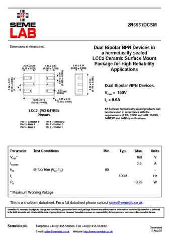
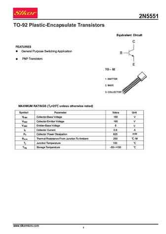
2N5551DCSM Dimensions in mm (inches). Dual Bipolar NPN Devices in a hermetically sealed LCC2 Ceramic Surface Mount Package for High Reliability 1.40 0.15 2.29 0.20 1.65 0.13 (0.055 0.006) (0.09 0.008) (0.065 0.005) Applications 2 3 1 4 Dual Bipolar NPN Devices. A 0.23 6 5 rad. (0.009) V = 160V CEO 6.22 0.13 A = 1.27 0.13 I = 0.6A C (0.
2n5551csm.pdf
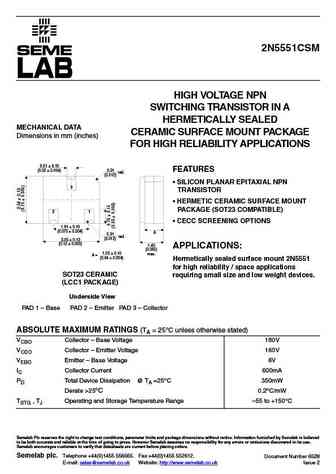
2N5551CSM HIGH VOLTAGE NPN SWITCHING TRANSISTOR IN A HERMETICALLY SEALED MECHANICAL DATA CERAMIC SURFACE MOUNT PACKAGE Dimensions in mm (inches) FOR HIGH RELIABILITY APPLICATIONS 0.51 0.10 (0.02 0.004) 0.31 FEATURES rad. (0.012) SILICON PLANAR EPITAXIAL NPN 3 TRANSISTOR HERMETIC CERAMIC SURFACE MOUNT PACKAGE (SOT23 COMPATIBLE) 21 CECC SCREENING OPTIONS 1.9
2n5551.pdf
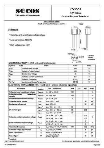
2N5551 NPN Silicon Elektronische Bauelemente General Purpose Transistor RoHS Compliant Product A suffix of "-C" specifies halogen & lead-free TO-92 4.55 0.2 3.5 0.2 FEATURES * Switching and amplification in high voltage * Low current(max. 600mA) * High voltage(max.180v) 0.43+0.08 0.07 46+0.1 0. 0.1 (1.27 Typ.) 1 Emitter +0.2 1.25 0.2 2 Base 1 2 3 3 Colle
2n5550.pdf
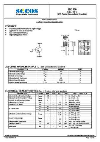
2N5550 0.6 A, 160 V NPN Plastic Encapsulated Transistor Elektronische Bauelemente RoHS Compliant Product A suffix of -C specifies halogen & lead-free FEATURES Switching and amplification in high voltage TO-92 Applications such as telephony Low current(max.600mA) High voltage(max.160V) G H J Millimeter REF. A D Min. Max. A 4.40 4.70 Collector B
2n5551.pdf
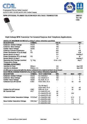
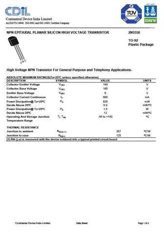
Continental Device India Limited An ISO/TS 16949, ISO 9001 and ISO 14001 Certified Company NPN EPITAXIAL PLANAR SILICON HIGH VOLTAGE TRANSISTOR 2N5551 TO- 92 CBE C B E High Voltage NPN Transistor For General Purpose And Telephony Applications. ABSOLUTE MAXIMUM RATINGS(Ta=25deg C unless otherwise specified) DESCRIPTION SYMBOL VALUE UNIT Collector -Emitter Voltage VCEO 160 V Collector
2n5550.pdf
Continental Device India Limited An ISO/TS 16949, ISO 9001 and ISO 14001 Certified Company NPN EPITAXIAL PLANAR SILICON HIGH VOLTAGE TRANSISTOR 2N5550 TO-92 Plastic Package High Voltage NPN Transistor For General Purpose and Telephony Applications. ABSOLUTE MAXIMUM RATINGS(Ta=25 C unless specified otherwise) DESCRIPTION SYMBOL VALUE UNITS VCEO Collector Emitter Voltage 140 V VCBO
2n5551.pdf
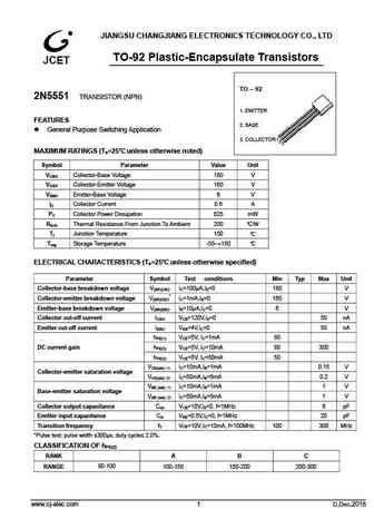
JIANGSU CHANGJIANG ELECTRONICS TECHNOLOGY CO., LTD TO-92 Plastic-Encapsulate Transistors TO 92 2N5551 TRANSISTOR (NPN) 1. EMITTER FEATURES 2. BASE General Purpose Switching Application 3. COLLECTOR MAXIMUM RATINGS (Ta=25 unless otherwise noted) Symbol Parameter Value Unit VCBO Collector-Base Voltage 180 V VCEO Collector-Emitter Voltage 160 V VEBO Emitter-Bas
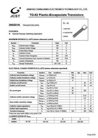
2n5551k.pdf
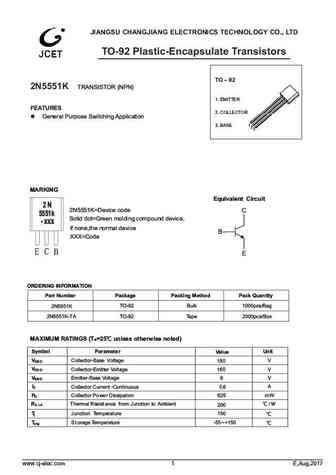
JIANGSU CHANGJIANG ELECTRONICS TECHNOLOGY CO., LTD TO-92 Plastic-Encapsulate Transistors TO 92 2N5551K TRANSISTOR (NPN) 1. EMITTER FEATURES 2. COLLECTOR General Purpose Switching Application 3. BASE Equivalent Circuit 2N5551K=Device code Solid dot=Green molding compound device, if none,the normal device XXX=Code
2n5550.pdf
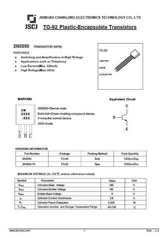
JIANGSU CHANGJING ELECTRONICS TECHNOLOGY CO., LTD TO-92 Plastic-Encapsulate Transistors 2N5550 TRANSISTOR (NPN) TO-92 FEATURES Switching and mplification in igh oltage 1.EMITTER Applications such as elephony Low urrent( ax. 600mA) 2.BASE High oltage( ax.160V) 3.COLLECTOR Equivalent Circuit 2N5550=Device code 2N Solid dot=Green molding compound device
2n5551.pdf
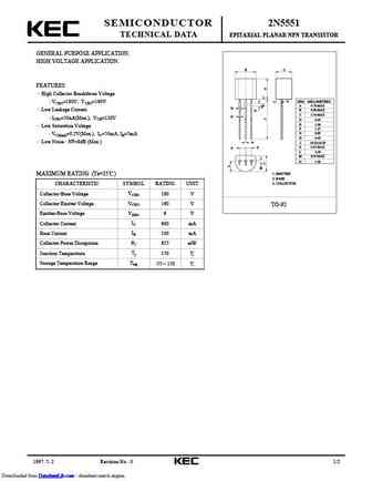
SEMICONDUCTOR 2N5551 TECHNICAL DATA EPITAXIAL PLANAR NPN TRANSISTOR GENERAL PURPOSE APPLICATION. HIGH VOLTAGE APPLICATION. B C FEATURES High Collector Breakdwon Voltage N DIM MILLIMETERS VCBO=180V, VCEO=160V A 4.70 MAX E K Low Leakage Current. B 4.80 MAX G C 3.70 MAX D ICBO=50nA(Max.), VCB=120V D 0.45 E 1.00 Low Saturation Voltage F 1.27 G 0.85 VCE(sat)=0.2V(Max.
2n5551s.pdf
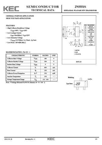
SEMICONDUCTOR 2N5551S TECHNICAL DATA EPITAXIAL PLANAR NPN TRANSISTOR GENERAL PURPOSE APPLICATION. HIGH VOLTAGE APPLICATION. E L B L DIM MILLIMETERS FEATURES _ + A 2.93 0.20 B 1.30+0.20/-0.15 High Collector Breakdwon Voltage C 1.30 MAX 2 VCBO=180V, VCEO=160V 3 D 0.40+0.15/-0.05 E 2.40+0.30/-0.20 Low Leakage Current. 1 G 1.90 H 0.95 ICBO=50nA(Max.) VCB=120V J 0.13+
2n5550.pdf
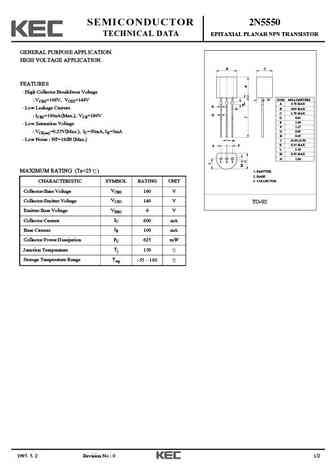
SEMICONDUCTOR 2N5550 TECHNICAL DATA EPITAXIAL PLANAR NPN TRANSISTOR GENERAL PURPOSE APPLICATION. HIGH VOLTAGE APPLICATION. B C FEATURES High Collector Breakdwon Voltage N DIM MILLIMETERS VCBO=160V, VCEO=140V A 4.70 MAX E K Low Leakage Current. B 4.80 MAX G C 3.70 MAX D ICBO=100nA(Max.), VCB=100V D 0.45 E 1.00 Low Saturation Voltage F 1.27 G 0.85 VCE(sat)=0.25V(Max.)
2n5550s.pdf
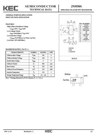
SEMICONDUCTOR 2N5550S TECHNICAL DATA EPITAXIAL PLANAR NPN TRANSISTOR GENERAL PURPOSE APPLICATION. HIGH VOLTAGE APPLICATION. E L B L DIM MILLIMETERS FEATURES _ + 2.93 0.20 A B 1.30+0.20/-0.15 High Collector Breakdwon Voltage C 1.30 MAX 2 VCBO=160V, VCEO=140V 3 D 0.45+0.15/-0.05 E 2.40+0.30/-0.20 Low Leakage Current. 1 G 1.90 H 0.95 ICBO=100nA(Max.) VCB=100V J 0.13+0.
2n5551c.pdf

SEMICONDUCTOR 2N5551C TECHNICAL DATA EPITAXIAL PLANAR NPN TRANSISTOR GENERAL PURPOSE APPLICATION. HIGH VOLTAGE APPLICATION. B C FEATURES High Collector Breakdwon Voltage N DIM MILLIMETERS VCBO=180V, VCEO=160V A 4.70 MAX E K Low Leakage Current. B 4.80 MAX G C 3.70 MAX D ICBO=50nA(Max.), VCB=120V D 0.45 E 1.00 Low Saturation Voltage F 1.27 G 0.85 VCE(sat)=0.2V(Max.),
2n5551sc.pdf
SEMICONDUCTOR 2N5551SC TECHNICAL DATA EPITAXIAL PLANAR NPN TRANSISTOR GENERAL PURPOSE APPLICATION. HIGH VOLTAGE APPLICATION. E L B L FEATURES High Collector Breakdwon Voltage DIM MILLIMETERS _ + A 2.90 0.1 2 3 VCBO=180V, VCEO=160V B 1.30+0.20/-0.15 C 1.30 MAX Low Leakage Current. 1 D 0.40+0.15/-0.05 ICBO=50nA(Max.) VCB=120V E 2.40+0.30/-0.20 G 1.90 Low Saturatio
2n5551.pdf
2N5551(NPN) TO-92 Bipolar Transistors TO-92 1. EMITTER 2. BASE 3. COLLECTOR Features Switching and amplification in high voltage Applications such as telephony Low current(max. 600mA) High voltage(max.180V) MAXIMUM RATINGS (TA=25 unless otherwise noted) Dimensions in inches and (millimeters) Symbol Parameter Value Units VCBO Collector-Base Voltage 180 V
2n5550.pdf
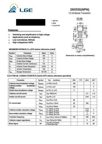
2N5550(NPN) TO-92 Bipolar Transistors TO-92 1. EMITTER 2. BASE 3. COLLECTOR Features Switching and amplification in high voltage Applications such as telephony Low current(max. 600mA) High voltage(max.160V) MAXIMUM RATINGS (TA=25 unless otherwise noted) Symbol Parameter Value Units Dimensions in inches and (millimeters) VCBO Collector-Base Voltage 160 V V
2n5551.pdf
2N5551 NPN Transistors TO-92 1. EMITTER 1 2 2. BASE 3 3. COLLECTOR ABSOLUTE MAXIMUM RATINGS (Ta=25 C) Rating Symbol 2N5551 Unit Collector-Emitter Voltage V CEO 160 Vdc Collector-Base Voltage VCBO 180 Vdc Emitter-Base VOltage VEBO 6.0 Vdc Collector Current IC 600 mAdc PD Total Device Dissipation T =25 C W A 0.625 Junction Temperature T 150 j C Storage, Temperature Tstg
h2n5551.pdf
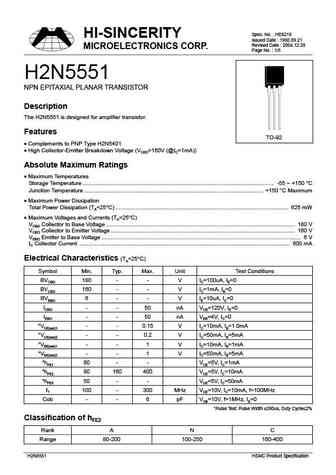
Spec. No. HE6219 HI-SINCERITY Issued Date 1992.09.21 Revised Date 2004.12.28 MICROELECTRONICS CORP. Page No. 1/5 H2N5551 NPN EPITAXIAL PLANAR TRANSISTOR Description The H2N5551 is designed for amplifier transistor. Features TO-92 Complements to PNP Type H2N5401 High Collector-Emitter Breakdown Voltage (VCEO>160V (@IC=1mA)) Absolute Maximum Ratings Maximum Temp
2n5551.pdf
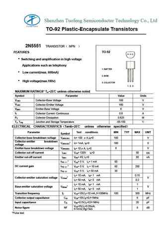
Shenzhen Tuofeng Semiconductor Technology Co., Ltd TO-92 Plastic-Encapsulate Transistors 2N5551 TRANSISTOR NPN TO-92 FEATURES Switching and amplification in high voltage Applications such as telephony 1. EMITTER Low current(max. 600mA) 2. BASE High voltage(max.180v) 3. COLLECTOR 1 2 3 MAXIMUM RATINGS* TA=25 unless otherwise noted Symbol Parame
2n5551.pdf
TO-92 Plastic-Encapsulate Transistors TO-92 TO-92 TO-92 TO-92 TRANSISTOR (NPN) 2N5551 TRANSISTOR (NPN) TRANSISTOR (NPN) TRANSISTOR (NPN) FEATURES FEATURES FEATURES FEATURES Switching and amplification in high voltage Switching and amplification in high voltage Switching and amplification in high voltage Switching and amplification in high voltage 1. EMlTTER
2n5551.pdf
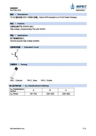
2N5551 Rev.F Mar.-2016 DATA SHEET / Descriptions TO-92 NPN Silicon NPN transistor in a TO-92 Plastic Package. / Features , 2N5401 High voltage, complementary Pair with 2N5401. / Applications General purpose high voltage amplifier. / Equival
2n5550 2n5551.pdf
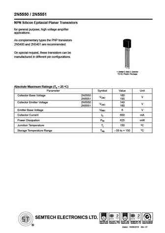
2N5550 / 2N5551 NPN Silicon Epitaxial Planar Transistors for general purpose, high voltage amplifier applications. As complementary types the PNP transistors 2N5400 and 2N5401 are recommended. On special request, these transistors can be manufactured in different pin configurations. 1. Emitter 2. Base 3. Collector TO-92 Plastic Package O Absolute Maximum Ratings (Ta = 25 C)
2n5551.pdf
SEMICONDUCTOR 2N5551 TECHNICAL DATA 2N5551 TRANSISTOR (NPN) B C FEATURES General Purpose Switching Application DIM MILLIMETERS A 4.70 MAX E B 4.80 MAX G C 3.70 MAX D MAXIMUM RATINGS (Ta=25 unless otherwise noted) D 0.55 MAX E 1.00 F 1.27 Symbol Parameter Value Unit G 0.85 H 0.45 VCBO Collector-Base Voltage 180 V _ H J 14.00 0.50 + L 2.30 F F VCEO Collector-E
2n5550-1s.pdf
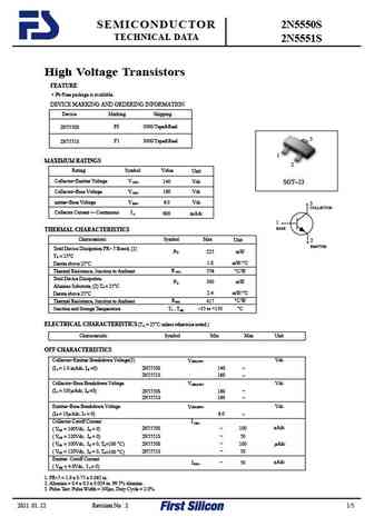
SEMICONDUCTOR 2N5550S TECHNICAL DATA 2N5551S High Voltage Transistors FEATURE Pb-Free package is available. DEVICE MARKING AND ORDERING INFORMATION Device Marking Shipping F0 3000/Tape&Reel 2N5550S 3 F1 3000/Tape&Reel 2N5551S 1 MAXIMUM RATINGS 2 Rating Symbol Value Unit Collector Emitter Voltage V CEO 140 Vdc SOT 23 Collector Base Voltage V CBO 160 Vdc
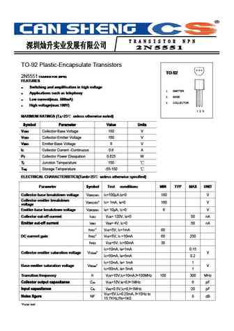
2n5551a.pdf
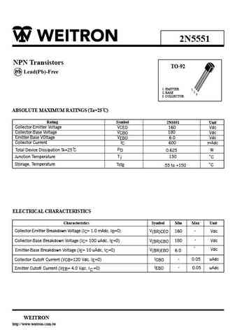
MAIN CHARACTERISTICS FEATURES IC 600mA Epitaxial silicon VCEO 160V High switching speed PC 625mW 2N5401A Complementary to 2N5401A RoHS RoHS product APPLICATIONS High frequency switch power supply Commonly power amplifier circuit
2n5551.pdf
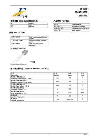
2N5551 TO-92 Plastic-Encapsulate Transistors Equivalent Circuit FEATURES General Purpose Switching Application PNP Transistors TO 92 1. EMITTER 2. BASE 3. COLLECTOR MAXIMUM RATINGS (Ta=25 unless otherwise noted) Symbol Parameter Value Unit VCBO Collector-Base Voltage 180 V VCEO Collector-Emitter Voltage 160 V VEBO Emitter-Base Voltage 6 V IC Collector Curre
2n5551.pdf
2N5551 TRANSISTOR (NPN) TO 92 FEATURES 1. EMITTER General Purpose Switching Application 2. BASE 3. COLLECTOR Equivalent Circuit 2N5551=Device code 2N XXX=Code 1 E B C ORDERING INFORMATION Part Number Package Packing Method Pack Quantity 2N5551 TO-92 Bulk 1000pcs/Bag 2N5551-TA TO-92 Tape 2000pcs/Box MAXIMUM RATINGS (Ta=25 unless otherwise
2n5551.pdf
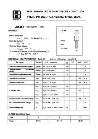
SHENZHEN HAOLIN ELECTRONICS TECHNOLOGY CO., LTD TO-92 Plastic-Encapsulate Transistors 2N5551 TRANSISTOR NPN TO 92 FEATURES Power dissipation PCM 0.625 W Tamb=25 1.EMITTER Collector current ICM 0.6 A 2.BASE Collector-base voltage 3.COLLECTOR V(BR)CBO 180 V 1 2 3 Operating and storage junction temperature range TJ Tstg -55 t
2n5419 2n5420 2n5550 2n5551 2n5830 2n5831 2n5832 2n5998 2n5999 2n6008 2n6009 2n6076 2n6426 2n6427.pdf
2n5551.pdf
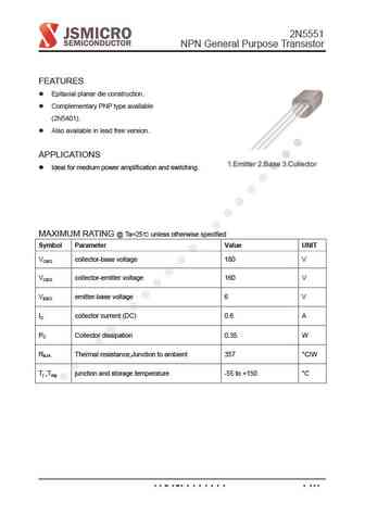
2N5551 NPN General Purpose Transistor FEATURES Epitaxial planar die construction. Complementary PNP type available (2N5401). Also available in lead free version. APPLICATIONS Ideal for medium power amplification and switching. MAXIMUM RATING @ Ta=25 unless otherwise specified Symbol Parameter Value UNIT VCBO collector-base voltage 180 V VCEO collector-emitter vo
2n5551u.pdf
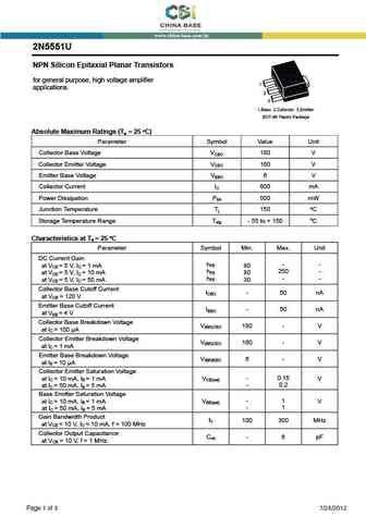
2N5551U NPN Silicon Epitaxial Planar Transistors for general purpose, high voltage amplifier applications. O Absolute Maximum Ratings (Ta = 25 C) Parameter Symbol Value Unit Collector Base Voltage VCBO 180 V Collector Emitter Voltage VCEO 160 V Emitter Base Voltage VEBO 6 V Collector Current IC 600 mA Power Dissipation Ptot 500 mW O Junction Temperature Tj 150 C O Storage T
Otros transistores... 2N5542, 2N555, 2N5550, 2N5551, 2N5552, 2N5552-1, 2N5552-2, 2N5552-4, TIP2955, 2N556, 2N5560, 2N557, 2N5575, 2N5576, 2N5577, 2N5578, 2N5579
🌐 : EN ES РУ

Liste
Recientemente añadidas las descripciónes de los transistores:
BJT: GA1A4M | SBT42 | 2SA200-Y | 2SA200-O | 2SD882-Q | 2SD882-P | 2SD882-E | 2SC945-L | 2SC945-H | 2SC4226-R23 | 2SC3357-F | 2SC3357-E | 2SC3356-R26 | 2SC3356-R24 | 2SC3356-R23 | 2SB772-Q | 2SB772-P | 2SB772-E | 2SA1015-L | 2SA1015-H | HSS8550
Popular searches
bcy21 | s8550 datasheet | mj50ac100 | 2sc1318 replacement | 2n3905 | mj15023 | tip36c transistor | 2sc3320