2N5626 Equivalente. Reemplazo. Hoja de especificaciones. Principales características
Número de Parte: 2N5626
Material: Si
Polaridad de transistor: NPN
ESPECIFICACIONES MÁXIMAS
Disipación total del dispositivo (Pc): 100 W
Tensión colector-base (Vcb): 100 V
Tensión colector-emisor (Vce): 80 V
Tensión emisor-base (Veb): 6 V
Corriente del colector DC máxima (Ic): 10 A
Temperatura operativa máxima (Tj): 200 °C
CARACTERÍSTICAS ELÉCTRICAS
Transición de frecuencia (fT): 40 MHz
Ganancia de corriente contínua (hFE): 70
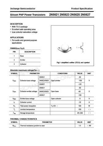
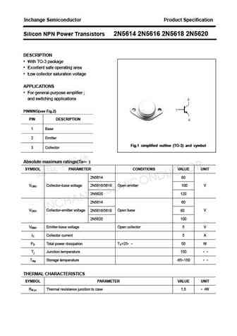
Encapsulados: TO3
Búsqueda de reemplazo de 2N5626
- Selecciónⓘ de transistores por parámetros
2N5626 datasheet
2n5622 2n5624 2n5626 2n5628.pdf
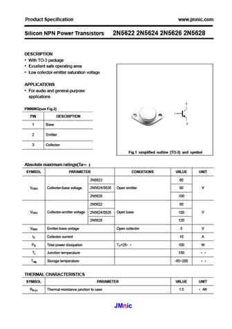
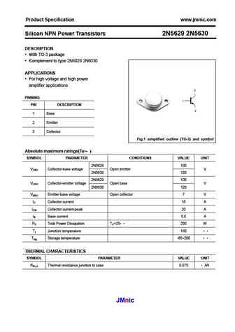
Product Specification www.jmnic.com Silicon NPN Power Transistors 2N5622 2N5624 2N5626 2N5628 DESCRIPTION With TO-3 package Excellent safe operating area Low collector-emitter saturation voltage APPLICATIONS For audio and general-purpose applications PINNING(see Fig.2) PIN DESCRIPTION 1 Base 2 Emitter 3 Collector Fig.1 simplified outline (TO-3) and symbol Abso
2n5622 2n5624 2n5626 2n5628.pdf
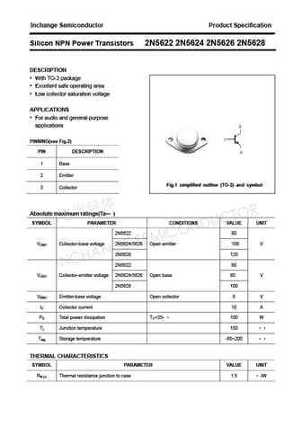
Inchange Semiconductor Product Specification Silicon NPN Power Transistors 2N5622 2N5624 2N5626 2N5628 DESCRIPTION With TO-3 package Excellent safe operating area Low collector saturation voltage APPLICATIONS For audio and general-purpose applications PINNING(see Fig.2) PIN DESCRIPTION 1 Base 2 Emitter Fig.1 simplified outline (TO-3) and symbol 3 Collector Abso
2n5629 2n5630 2n6029 2n6030.pdf
145 Adams Avenue, Hauppauge, NY 11788 USA Tel (631) 435-1110 Fax (631) 435-1824
2n5620.pdf
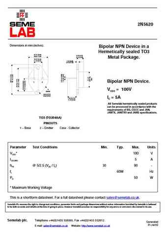
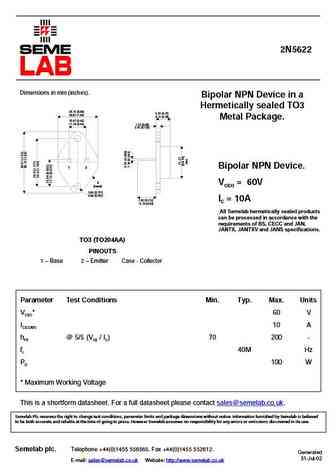
2N5620 Dimensions in mm (inches). Bipolar NPN Device in a Hermetically sealed TO3 25.15 (0.99) 6.35 (0.25) 26.67 (1.05) 9.15 (0.36) Metal Package. 10.67 (0.42) 11.18 (0.44) 1.52 (0.06) 3.43 (0.135) 1 2 Bipolar NPN Device. 3 VCEO = 100V (case) 3.84 (0.151) 4.09 (0.161) 7.92 (0.312) IC = 5A 12.70 (0.50) All Semelab hermetically sealed products can be processed in a

Otros transistores... 2N5618 , 2N5619 , 2N5620 , 2N5621 , 2N5622 , 2N5623 , 2N5624 , 2N5625 , 2SD1047 , 2N5627 , 2N5628 , 2N5629 , 2N563 , 2N5630 , 2N5631 , 2N5632 , 2N5633 .
🌐 : EN ES РУ

Liste
Recientemente añadidas las descripciónes de los transistores:
BJT: GA1A4M | SBT42 | 2SA200-Y | 2SA200-O | 2SD882-Q | 2SD882-P | 2SD882-E | 2SC945-L | 2SC945-H | 2SC4226-R23 | 2SC3357-F | 2SC3357-E | 2SC3356-R26 | 2SC3356-R24 | 2SC3356-R23 | 2SB772-Q | 2SB772-P | 2SB772-E | 2SA1015-L | 2SA1015-H | HSS8550
Popular searches
irfp264 | ksc2690 | bc546 datasheet | mpsa06 transistor | tta004b | 2sc1116 | 2n3565 equivalent | 10n60