APT43GA90BD30 Specs and Replacement
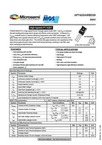
Type Designator: APT43GA90BD30
Type: IGBT
Type of IGBT Channel: N
Absolute Maximum Ratings
Pc ⓘ - Maximum Power Dissipation: 337 W
|Vce|ⓘ - Maximum Collector-Emitter Voltage: 900 V
|Vge|ⓘ - Maximum Gate-Emitter Voltage: 30 V
|Ic| ⓘ - Maximum Collector Current: 43 A @25℃
Tj ⓘ - Maximum Junction Temperature: 150 ℃
Electrical Characteristics
|VCEsat|ⓘ - Collector-Emitter saturation Voltage, typ: 2.2 V @25℃
tr ⓘ - Rise Time, typ: 16 nS
Coesⓘ - Output Capacitance, typ: 227 pF
Package: TO247
APT43GA90BD30 Substitution - IGBT ⓘ Cross-Reference Search
APT43GA90BD30 datasheet
apt43ga90bd30.pdf
APT43GA90BD30 900V High Speed PT IGBT POWER MOS 8 is a high speed Punch-Through switch-mode IGBT. Low Eoff is achieved through leading technology silicon design and lifetime control processes. A reduced Eoff - VCE(ON) tradeoff results in superior efficiency compared to other IGBT technologies. Low APT43GA90B gate charge and a greatly reduced ratio of Cres/Cies provide excellent n... See More ⇒
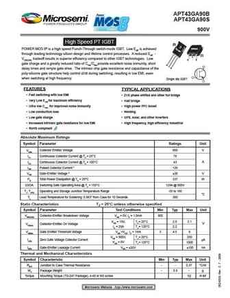
apt43ga90b apt43ga90s.pdf
APT43GA90B APT43GA90S 900V High Speed PT IGBT (B) POWER MOS 8 is a high speed Punch-Through switch-mode IGBT. Low Eoff is achieved D3PAK through leading technology silicon design and lifetime control processes. A reduced Eoff - (S) C VCE(ON) tradeoff results in superior efficiency compared to other IGBT technologies. Low G E gate charge and a greatly reduced ratio of Cres/Cie... See More ⇒
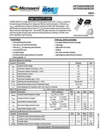
apt43ga90sd30.pdf
APT43GA90BD30 APT43GA90SD30 900V High Speed PT IGBT (B) D3PAK POWER MOS 8 is a high speed Punch-Through switch-mode IGBT. Low Eoff is achieved through leading technology silicon design and lifetime control processes. A reduced Eoff - (S) C G E VCE(ON) tradeoff results in superior efficiency compared to other IGBT technologies. Low gate charge and a greatly reduced ratio of ... See More ⇒
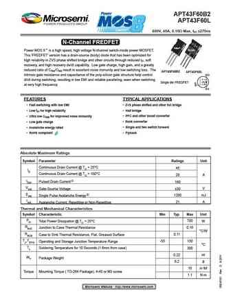
apt43f60b2 apt43f60l.pdf
APT43F60B2 APT43F60L 600V, 45A, 0.15 Max, trr 270ns N-Channel FREDFET T-Max TO-264 Power MOS 8 is a high speed, high voltage N-channel switch-mode power MOSFET. This 'FREDFET' version has a drain-source (body) diode that has been optimized for high reliability in ZVS phase shifted bridge and other circuits through reduced trr, soft recovery, and high recovery dv/dt cap... See More ⇒
Specs: APT50GP60JDQ2 , TGAN30N120FD , TGH30N120FD , APT44GA60B , APT44GA60BD30 , APT44GA60S , APT44GA60SD30 , APT43GA90B , GT30G124 , APT43GA90S , APT43GA90SD30 , VS-EMG050J60N , VS-EMF050J60U , APT40GT60BRG , APT25GT120BRG , APT40GF120JRDQ2 , 70MT060WHTAPBF .
History: RJH1BF7RDPQ-80
Keywords - APT43GA90BD30 transistor spec
APT43GA90BD30 cross reference
APT43GA90BD30 equivalent finder
APT43GA90BD30 lookup
APT43GA90BD30 substitution
APT43GA90BD30 replacement
History: RJH1BF7RDPQ-80
🌐 : EN ES РУ
LIST
Last Update
IGBT: JJT40N120SE | JJT40N120HE | JJT30N65UE
Popular searches
2n5401 datasheet | mj21194g | irfz34n | mn2488 | irfb438 | mj21193g | irf3710 pinout | irf9530 datasheet
