APT1001R3HN Specs and Replacement
Type Designator: APT1001R3HN
Type of Transistor: MOSFET
Type of Control Channel: N-Channel
Absolute Maximum Ratings
Pd ⓘ
- Maximum Power Dissipation: 250 W
|Vds|ⓘ - Maximum Drain-Source Voltage: 1000 V
|Vgs|ⓘ - Maximum Gate-Source Voltage: 30 V
|Id| ⓘ - Maximum Drain Current: 9 A
Tj ⓘ - Maximum Junction Temperature: 150 °C
Electrical Characteristics
RDSonⓘ - Maximum Drain-Source On-State Resistance: 1.3 Ohm
Package: TO258
- MOSFET ⓘ Cross-Reference Search
APT1001R3HN datasheet
6.1. Size:68K apt
apt1001r1avr.pdf 
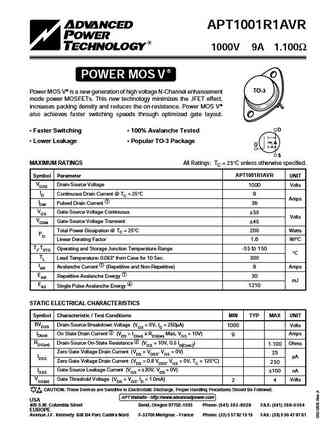
APT1001R1AVR 1000V 9A 1.100 POWER MOS V TO-3 Power MOS V is a new generation of high voltage N-Channel enhancement mode power MOSFETs. This new technology minimizes the JFET effect, increases packing density and reduces the on-resistance. Power MOS V also achieves faster switching speeds through optimized gate layout. D Faster Switching 100% Avalanche Tested Lower... See More ⇒
6.2. Size:34K apt
apt1001rblc.pdf

APT1001RBLC APT1001RSLC 1000V 11A 1.000W BLC TM POWER MOS VI D3PAK Power MOS VITM is a new generation of low gate charge, high voltage TO-247 N-Channel enhancement mode power MOSFETs. Lower gate charge is achieved by optimizing the manufacturing process to minimize Ciss and Crss. Lower gate charge coupled with Power MOS VITM optimized gate layout, SLC delivers exceptionally fast sw... See More ⇒
6.3. Size:63K apt
apt1001rsvrg.pdf
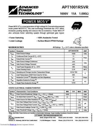
APT1001RSVR 1000V 11A 1.000 POWER MOS V D3PAK Power MOS V is a new generation of high voltage N-Channel enhancement mode power MOSFETs. This new technology minimizes the JFET effect, increases packing density and reduces the on-resistance. Power MOS V also achieves faster switching speeds through optimized gate layout. D Faster Switching 100% Avalanche Tested Lowe... See More ⇒
6.4. Size:70K apt
apt1001r1bvfr.pdf
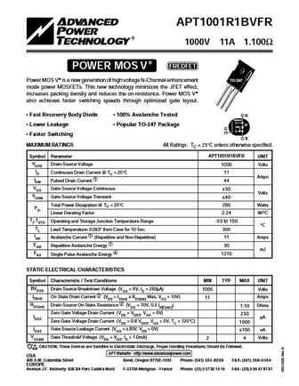
APT1001R1BVFR 1000V 11A 1.100 POWER MOS V FREDFET Power MOS V is a new generation of high voltage N-Channel enhancement TO-247 mode power MOSFETs. This new technology minimizes the JFET effect, increases packing density and reduces the on-resistance. Power MOS V also achieves faster switching speeds through optimized gate layout. Fast Recovery Body Diode 100% Avalanche T... See More ⇒
6.5. Size:68K apt
apt1001rbvr.pdf
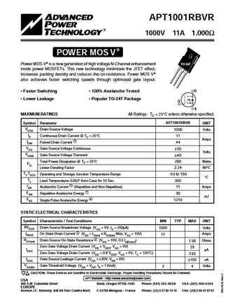
APT1001RBVR 1000V 11A 1.000 POWER MOS V Power MOS V is a new generation of high voltage N-Channel enhancement TO-247 mode power MOSFETs. This new technology minimizes the JFET effect, increases packing density and reduces the on-resistance. Power MOS V also achieves faster switching speeds through optimized gate layout. D Faster Switching 100% Avalanche Tested Lowe... See More ⇒
6.6. Size:118K apt
apt1001rbvfr.pdf

APT1001RBVFR APT1001RSVFR 1000V 11A 1.00 BVFR POWER MOS V FREDFET D3PAK TO-247 Power MOS V is a new generation of high voltage N-Channel enhancement mode power MOSFETs. This new technology minimizes the JFET effect, increases packing density and reduces the on-resistance. Power MOS V SVFR also achieves faster switching speeds through optimized gate layou... See More ⇒
6.7. Size:67K apt
apt1001r1hvr.pdf
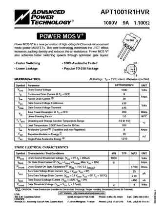
APT1001R1HVR 1000V 9A 1.100 POWER MOS V TO-258 Power MOS V is a new generation of high voltage N-Channel enhancement mode power MOSFETs. This new technology minimizes the JFET effect, increases packing density and reduces the on-resistance. Power MOS V also achieves faster switching speeds through optimized gate layout. D Faster Switching 100% Avalanche Tested Low... See More ⇒
6.8. Size:50K apt
apt1001r6bn.pdf
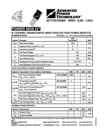
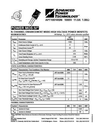
D TO-247 G APT1001R6BN 1000V 8.0A 1.60 S APT1002R4BN 1000V 6.5A 2.40 POWER MOS IV N- CHANNEL ENHANCEMENT MODE HIGH VOLTAGE POWER MOSFETS MAXIMUM RATINGS All Ratings TC = 25 C unless otherwise specified. APT APT Symbol Parameter 1001R6BN 1002R4BN UNIT VDSS Drain-Source Voltage 1000 1000 Volts ID Continuous Drain Current @ TC = 25 C 8 6.5 Amps IDM Pulsed Drain Current 1... See More ⇒
6.9. Size:150K apt
apt1001r6bfllg apt1001r6sfllg.pdf
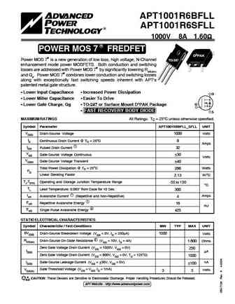
Typical Performance Curves APT1001R6BFLL_SFLL APT1001R6BFLL APT1001R6SFLL 1000V 8A 1.60 R POWER MOS 7 FREDFET D3PAK Power MOS 7 is a new generation of low loss, high voltage, N-Channel TO-247 enhancement mode power MOSFETS. Both conduction and switching losses are addressed with Power MOS 7 by significantly lowering RDS(ON) and Qg. Power MOS 7 combines ... See More ⇒
6.10. Size:52K apt
apt1001r1bn.pdf
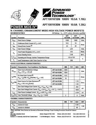
D TO-247 G APT1001R1BN 1000V 10.5A 1.10 S APT1001R3BN 1000V 10.0A 1.30 POWER MOS IV N- CHANNEL ENHANCEMENT MODE HIGH VOLTAGE POWER MOSFETS MAXIMUM RATINGS All Ratings TC = 25 C unless otherwise specified. APT APT Symbol Parameter 1001RBN 1001R3BN UNIT VDSS Drain-Source Voltage 1000 1000 Volts ID Continuous Drain Current @ TC = 25 C 10.5 10 Amps IDM Pulsed Drain Curren... See More ⇒
6.11. Size:71K apt
apt1001rsvr.pdf
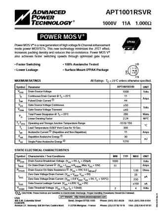
APT1001RSVR 1000V 11A 1.000 POWER MOS V D3PAK Power MOS V is a new generation of high voltage N-Channel enhancement mode power MOSFETs. This new technology minimizes the JFET effect, increases packing density and reduces the on-resistance. Power MOS V also achieves faster switching speeds through optimized gate layout. D Faster Switching 100% Avalanche Tested Lowe... See More ⇒
6.12. Size:34K apt
apt1001rslc.pdf
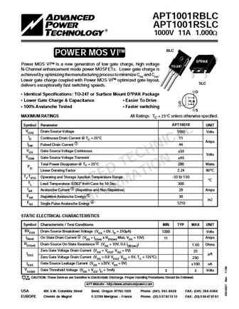
APT1001RBLC APT1001RSLC 1000V 11A 1.000W BLC TM POWER MOS VI D3PAK Power MOS VITM is a new generation of low gate charge, high voltage TO-247 N-Channel enhancement mode power MOSFETs. Lower gate charge is achieved by optimizing the manufacturing process to minimize Ciss and Crss. Lower gate charge coupled with Power MOS VITM optimized gate layout, SLC delivers exceptionally fast sw... See More ⇒
6.13. Size:139K apt
apt1001rsvfr.pdf
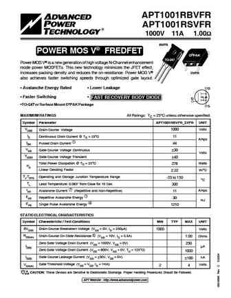
APT1001RBVFR APT1001RSVFR 1000V 11A 1.00 BVFR POWER MOS V FREDFET D3PAK TO-247 Power MOS V is a new generation of high voltage N-Channel enhancement mode power MOSFETs. This new technology minimizes the JFET effect, increases packing density and reduces the on-resistance. Power MOS V SVFR also achieves faster switching speeds through optimized gate layou... See More ⇒
6.14. Size:51K apt
apt1001rbn.pdf
D TO-247 G APT1001RBN 1000V 11.0A 1.00 S APT5030BN 500V 21.0A 0.30 POWER MOS IV N- CHANNEL ENHANCEMENT MODE HIGH VOLTAGE POWER MOSFETS MAXIMUM RATINGS All Ratings TC = 25 C unless otherwise specified. APT Symbol Parameter 1001RBN UNIT VDSS Drain-Source Voltage 1000 Volts ID Continuous Drain Current @ TC = 25 C 11 Amps IDM Pulsed Drain Current 1 44 VGS Gate-Source Vo... See More ⇒
Detailed specifications: APT1001R1BVFR, APT1001R1HN, APT1001R1HVR, APT1001R2AN, APT1001R2BN, APT1001R2HN, APT1001R3AN, APT1001R3BN, AON7408, APT1001R6BN, APT1001RAN, APT1001RBN, APT1001RBVR, APT1001RSVR, APT10025JVFR, APT10025JVR, APT10025PVR
Keywords - APT1001R3HN MOSFET specs
APT1001R3HN cross reference
APT1001R3HN equivalent finder
APT1001R3HN pdf lookup
APT1001R3HN substitution
APT1001R3HN replacement
Need a MOSFET replacement?
Our guide shows you how to find a perfect substitute by comparing key parameters and specs
