APT10M19BVR Specs and Replacement
Type Designator: APT10M19BVR
Type of Transistor: MOSFET
Type of Control Channel: N-Channel
Absolute Maximum Ratings
Pd ⓘ - Maximum Power Dissipation: 370 W
|Vds|ⓘ - Maximum Drain-Source Voltage: 100 V
|Vgs|ⓘ - Maximum Gate-Source Voltage: 30 V
|Id| ⓘ - Maximum Drain Current: 75 A
Tj ⓘ - Maximum Junction Temperature: 150 °C
Electrical Characteristics
tr ⓘ - Rise Time: 40 nS
Cossⓘ - Output Capacitance: 1900 pF
RDSonⓘ - Maximum Drain-Source On-State Resistance: 0.019 Ohm
Package: TO247
APT10M19BVR substitution
- MOSFET ⓘ Cross-Reference Search
APT10M19BVR datasheet
apt10m19bvr.pdf

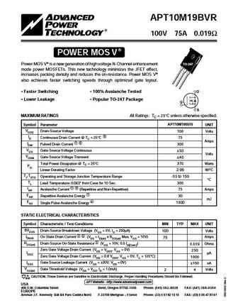
APT10M19BVR 100V 75A 0.019 POWER MOS V Power MOS V is a new generation of high voltage N-Channel enhancement TO-247 mode power MOSFETs. This new technology minimizes the JFET effect, increases packing density and reduces the on-resistance. Power MOS V also achieves faster switching speeds through optimized gate layout. Faster Switching 100% Avalanche Tested D Lower ... See More ⇒
apt10m19bvr.pdf
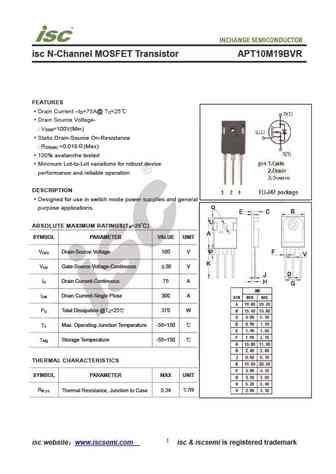
isc N-Channel MOSFET Transistor APT10M19BVR FEATURES Drain Current I =75A@ T =25 D C Drain Source Voltage- V =100V(Min) DSS Static Drain-Source On-Resistance R =0.019 (Max) DS(on) 100% avalanche tested Minimum Lot-to-Lot variations for robust device performance and reliable operation DESCRIPTION Designed for use in switch mode power supplies and general pur... See More ⇒
apt10m19bvrg.pdf
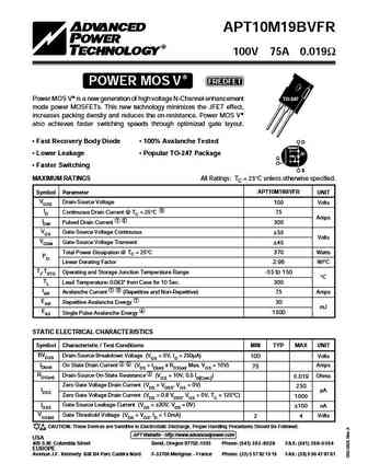
APT10M19BVR 100V 75A 0.019 POWER MOS V Power MOS V is a new generation of high voltage N-Channel enhancement TO-247 mode power MOSFETs. This new technology minimizes the JFET effect, increases packing density and reduces the on-resistance. Power MOS V also achieves faster switching speeds through optimized gate layout. Faster Switching 100% Avalanche Tested D Lower ... See More ⇒
apt10m19bvfr.pdf
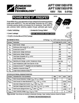
APT10M19BVFR 100V 75A 0.019 POWER MOS V FREDFET TO-247 Power MOS V is a new generation of high voltage N-Channel enhancement TO-247 mode power MOSFETs. This new technology minimizes the JFET effect, increases packing density and reduces the on-resistance. Power MOS V also achieves faster switching speeds through optimized gate layout. Fast Recovery Body Diode 100% Avala... See More ⇒
Detailed specifications: APT10086BVR , APT10086SVR , APT10088HVR , APT10M07JVR , APT10M11B2VR , APT10M11JVR , APT10M11LVR , APT10M19BVFR , 8N60 , APT10M19SVR , APT10M25BVFR , APT10M25BVR , APT10M25SVR , APT1201R5BVR , APT1201R6BVR , APT12040JVR , APT12080JVR .
History: SI2328 | SIA519 | RSS130N03TB
Keywords - APT10M19BVR MOSFET specs
APT10M19BVR cross reference
APT10M19BVR equivalent finder
APT10M19BVR pdf lookup
APT10M19BVR substitution
APT10M19BVR replacement
Step-by-step guide to finding a MOSFET replacement. Cross-reference parts and ensure compatibility for your repair or project.
History: SI2328 | SIA519 | RSS130N03TB
🌐 : EN ES РУ

LIST
Last Update
MOSFET: ASD80R750E | ASD70R950E | ASD70R600E | ASD70R380E | ASD65R850E | ASD65R550E | ASD65R350E | ASD65R300E | ASD65R280E | ASD65R270E
Popular searches
irf9630 | mj2955 | mje15030 | 2n3904 transistor | 2sd424 | 2sc828 | 2n4125 | tip42c transistor