APT4012BVR Specs and Replacement
Type Designator: APT4012BVR
Type of Transistor: MOSFET
Type of Control Channel: N-Channel
Absolute Maximum Ratings
Pd ⓘ - Maximum Power Dissipation: 370 W
|Vds|ⓘ - Maximum Drain-Source Voltage: 400 V
|Vgs|ⓘ - Maximum Gate-Source Voltage: 30 V
|Id| ⓘ - Maximum Drain Current: 37 A
Tj ⓘ - Maximum Junction Temperature: 150 °C
Electrical Characteristics
tr ⓘ - Rise Time: 17 nS
Cossⓘ - Output Capacitance: 690 pF
RDSonⓘ - Maximum Drain-Source On-State Resistance: 0.12 Ohm
Package: TO247
APT4012BVR substitution
- MOSFET ⓘ Cross-Reference Search
APT4012BVR datasheet
apt4012bvr.pdf
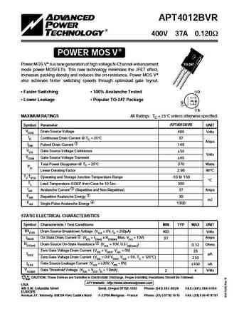
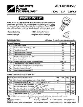
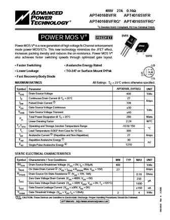
APT4012BVR 400V 37A 0.120 POWER MOS V Power MOS V is a new generation of high voltage N-Channel enhancement TO-247 mode power MOSFETs. This new technology minimizes the JFET effect, increases packing density and reduces the on-resistance. Power MOS V also achieves faster switching speeds through optimized gate layout. Faster Switching 100% Avalanche Tested D Lower L... See More ⇒
apt4012bvfrg apt4012svfrg.pdf
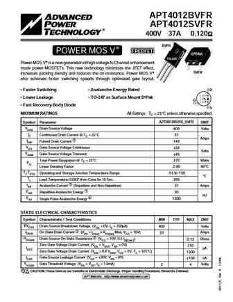
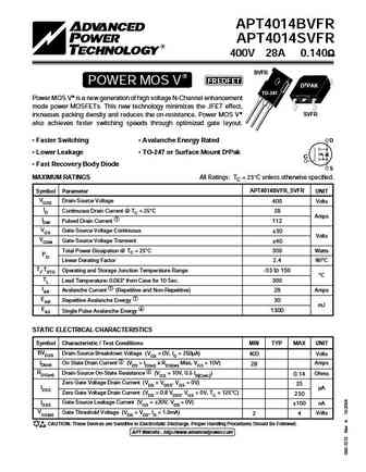
APT4012BVFR APT4012SVFR 400V 37A 0.120 BVFR FREDFET POWER MOS V D3PAK TO-247 Power MOS V is a new generation of high voltage N-Channel enhancement mode power MOSFETs. This new technology minimizes the JFET effect, SVFR increases packing density and reduces the on-resistance. Power MOS V also achieves faster switching speeds through optimized gate layout.... See More ⇒
apt4016bn.pdf
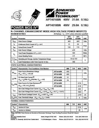
D TO-247 G APT4016BN 400V 31.0A 0.16 S APT4018BN 400V 29.0A 0.18 POWER MOS IV N- CHANNEL ENHANCEMENT MODE HIGH VOLTAGE POWER MOSFETS MAXIMUM RATINGS All Ratings TC = 25 C unless otherwise specified. APT APT Symbol Parameter 4016BN 4018BN UNIT VDSS Drain-Source Voltage 400 400 Volts ID Continuous Drain Current @ TC = 25 C 31 29 Amps IDM Pulsed Drain Current 1 124 116 ... See More ⇒
apt4014bvr.pdf
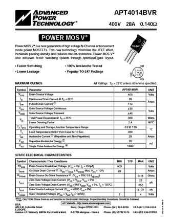
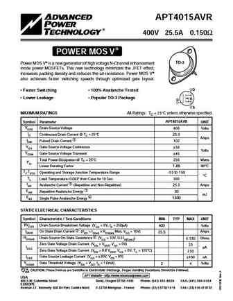
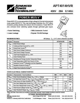
APT4014BVR 400V 28A 0.140 POWER MOS V Power MOS V is a new generation of high voltage N-Channel enhancement TO-247 mode power MOSFETs. This new technology minimizes the JFET effect, increases packing density and reduces the on-resistance. Power MOS V also achieves faster switching speeds through optimized gate layout. Faster Switching 100% Avalanche Tested D Lower L... See More ⇒


Detailed specifications: APT30M40JVR, APT30M40LVFR, APT30M40LVR, APT30M70BVFR, APT30M70BVR, APT30M85BVFR, APT30M85BVR, APT30M90AVR, AO3400, APT4014BVR, APT4014HVR, APT4015AVR, APT4016BN, APT4016BVR, APT4018HVR, APT4020BN, APT4020BVR
Keywords - APT4012BVR MOSFET specs
APT4012BVR cross reference
APT4012BVR equivalent finder
APT4012BVR pdf lookup
APT4012BVR substitution
APT4012BVR replacement
Learn how to find the right MOSFET substitute. A guide to cross-reference, check specs and replace MOSFETs in your circuits.
🌐 : EN ES РУ

LIST
Last Update
MOSFET: AUW033N08BG | AUW025N10 | AUR030N10 | AUR020N10 | AUR020N085 | AUR014N10 | AUP074N10 | AUP065N10 | AUP062N08BG | AUP060N08AG
Popular searches
irfz34n | mn2488 | irfb438 | mj21193g | irf3710 pinout | irf9530 datasheet | mj21194 | oc71 transistor