IPB108N15N3G Specs and Replacement
Type Designator: IPB108N15N3G
Type of Transistor: MOSFET
Type of Control Channel: N-Channel
Absolute Maximum Ratings
Pd ⓘ
- Maximum Power Dissipation: 214 W
|Vds|ⓘ - Maximum Drain-Source Voltage: 150 V
|Vgs|ⓘ - Maximum Gate-Source Voltage: 20 V
|Id| ⓘ - Maximum Drain Current: 83 A
Tj ⓘ - Maximum Junction Temperature: 175 °C
Electrical Characteristics
tr ⓘ - Rise Time: 35 nS
Cossⓘ -
Output Capacitance: 378 pF
RDSonⓘ - Maximum Drain-Source On-State Resistance: 0.0108 Ohm
Package: TO263
IPB108N15N3G substitution
- MOSFET ⓘ Cross-Reference Search
IPB108N15N3G datasheet
..1. Size:757K infineon
ipb108n15n3g ipp111n15n3g ipi111n15n3g.pdf 

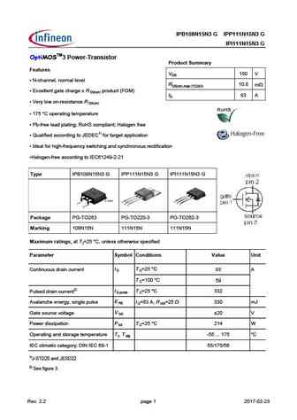
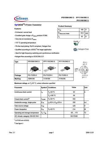
IPB108N15N3 G IPP111N15N3 G IPI111N15N3 G OptiMOSTM3 Power-Transistor Product Summary Features VDS 150 V N-channel, normal level RDS(on),max (TO263) 10.8 mW Excellent gate charge x R product (FOM) DS(on) ID 83 A Very low on-resistance R DS(on) 175 C operating temperature Pb-free lead plating; RoHS compliant; Halogen free Qualified according to JEDE... See More ⇒
..2. Size:258K inchange semiconductor
ipb108n15n3g.pdf 

Isc N-Channel MOSFET Transistor IPB108N15N3G FEATURES With To-263(D2PAK) package Low input capacitance and gate charge Low gate input resistance 100% avalanche tested Minimum Lot-to-Lot variations for robust device performance and reliable operation APPLICATIONS Switching applications ABSOLUTE MAXIMUM RATINGS(T =25 ) a SYMBOL PARAMETER VALUE UNIT V Drain-Source ... See More ⇒
3.1. Size:438K infineon
ipb108n15n3-g ipp111n15n3-g ipi111n15n3-g.pdf 

IPB108N15N3 G IPP111N15N3 G IPI111N15N3 G OptiMOSTM3 Power-Transistor Product Summary Features V 150 V DS N-channel, normal level R 10.8 m DS(on),max (TO263) Excellent gate charge x R product (FOM) DS(on) I 83 A D Very low on-resistance R DS(on) 175 C operating temperature Pb-free lead plating; RoHS compliant; Halogen free Qualified according to JE... See More ⇒
9.1. Size:186K infineon
ipb100n10s3-05 ipi100n10s3-05 ipp100n10s3-05.pdf 

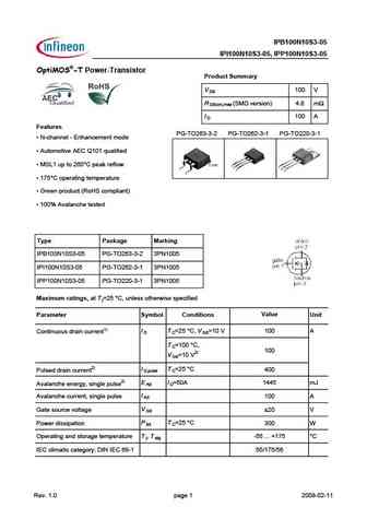
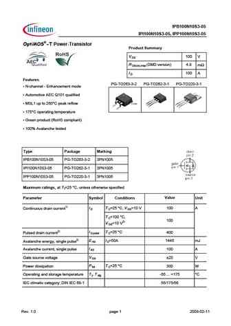
IPB100N10S3-05 IPI100N10S3-05, IPP100N10S3-05 OptiMOS -T Power-Transistor Product Summary V 100 V DS R (SMD version) 4.8 m DS(on),max I 100 A D Features PG-TO263-3-2 PG-TO262-3-1 PG-TO220-3-1 N-channel - Enhancement mode Automotive AEC Q101 qualified MSL1 up to 260 C peak reflow 175 C operating temperature Green product (RoHS compliant) 100% Aval... See More ⇒
9.2. Size:159K infineon
ipb100n06s2l-05 ipp100n06s2l-05.pdf 

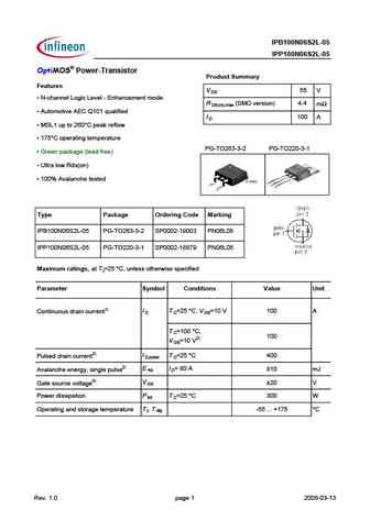
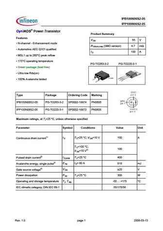
IPB100N06S2L-05 IPP100N06S2L-05 OptiMOS Power-Transistor Product Summary Features V 55 V DS N-channel Logic Level - Enhancement mode R (SMD version) 4.4 m DS(on),max Automotive AEC Q101 qualified I 100 A D MSL1 up to 260 C peak reflow 175 C operating temperature PG-TO263-3-2 PG-TO220-3-1 Green package (lead free) Ultra low Rds(on) 100% Avala... See More ⇒
9.3. Size:159K infineon
ipp100n04s4-h2 ipb100n04s4-h2 ipi100n04s4-h2.pdf 

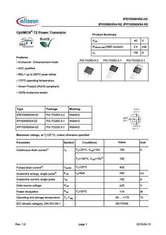
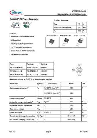
IPB100N04S4-H2 IPI100N04S4-H2, IPP100N04S4-H2 OptiMOS -T2 Power-Transistor Product Summary V 40 V DS R (SMD version) 2.4 m DS(on),max I 100 A D Features PG-TO263-3-2 PG-TO262-3-1 PG-TO220-3-1 N-channel - Enhancement mode AEC qualified MSL1 up to 260 C peak reflow 175 C operating temperature Green Product (RoHS compliant) 100% Avalanche tested Ty... See More ⇒
9.4. Size:652K infineon
ipb107n20na ipp110n20na.pdf 

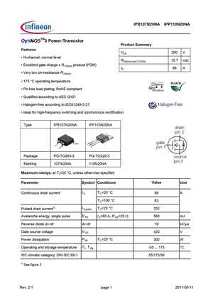
IPB107N20NA IPP110N20NA OptiMOSTM3 Power-Transistor Product Summary Features VDS 200 V N-channel, normal level RDS(on),max (TO263) 10.7 mW Excellent gate charge x R product (FOM) DS(on) ID 88 A Very low on-resistance R DS(on) 175 C operating temperature Pb-free lead plating; RoHS compliant Qualified according to AEC Q101 Halogen-free according to IE... See More ⇒
9.6. Size:153K infineon
ipb100n04s2-04 ipp100n04s2-04 ipp100n04s2-04 ipb100n04s2-04.pdf 

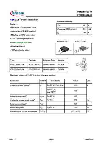
IPB100N04S2-04 IPP100N04S2-04 OptiMOS Power-Transistor Product Summary Features V 40 V DS N-channel - Enhancement mode R (SMD version) 3.3 m DS(on),max Automotive AEC Q101 qualified I 100 A D MSL1 up to 260 C peak reflow 175 C operating temperature PG-TO263-3-2 PG-TO220-3-1 Green package (lead free) Ultra low Rds(on) 100% Avalanche tested T... See More ⇒
9.7. Size:195K infineon
ipb100n06s3-04.pdf 

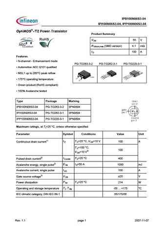
IPB100N06S3-04 IPI100N06S3-04, IPP100N06S3-04 OptiMOS -T2 Power-Transistor Product Summary V 55 V DS R (SMD version) 4.1 m DS(on),max I 100 A D Features N-channel - Enhancement mode PG-TO263-3-2 PG-TO262-3-1 PG-TO220-3-1 Automotive AEC Q101 qualified MSL1 up to 260 C peak reflow 175 C operating temperature Green product (RoHS compliant) 100% Avala... See More ⇒
9.8. Size:690K infineon
ipb107n20n3-g ipp110n20n3-g ipi110n20n3-g ipb107n20n3g ipp110n20n3g ipi110n20n3g.pdf 

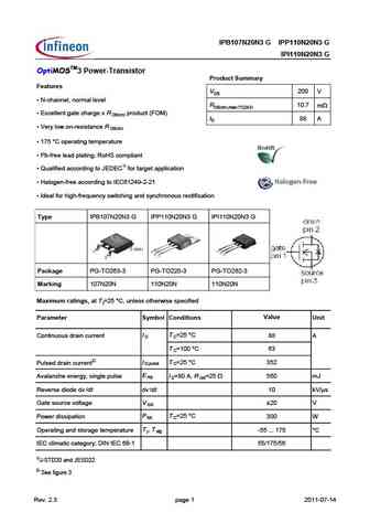
IPB107N20N3 G IPP110N20N3 G IPI110N20N3 G OptiMOSTM3 Power-Transistor Product Summary Features VDS 200 V N-channel, normal level RDS(on),max (TO263) 10.7 mW Excellent gate charge x R product (FOM) DS(on) ID 88 A Very low on-resistance R DS(on) 175 C operating temperature Pb-free lead plating; RoHS compliant Qualified according to JEDEC1) for target appl... See More ⇒
9.9. Size:135K infineon
ipb100n04s4-h2 ipi100n04s4-h2 ipp100n04s4-h2.pdf 

IPB100N04S4-H2 IPI100N04S4-H2, IPP100N04S4-H2 OptiMOS -T2 Power-Transistor Product Summary V 40 V DS R (SMD version) 2.4 mW DS(on),max I 100 A D Features PG-TO263-3-2 PG-TO262-3-1 PG-TO220-3-1 N-channel - Enhancement mode AEC qualified MSL1 up to 260 C peak reflow 175 C operating temperature Green Product (RoHS compliant) 100% Avalanche tested Type ... See More ⇒
9.11. Size:154K infineon
ipb100n08s2l-07 ipp100n08s2l-07 ipp100n08s2l-07 ipb100n08s2l-07.pdf 

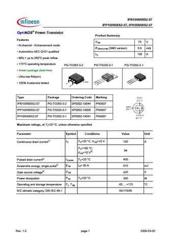
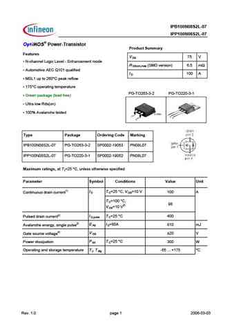
IPB100N08S2L-07 IPP100N08S2L-07 OptiMOS Power-Transistor Product Summary Features V 75 V DS N-channel Logic Level - Enhancement mode R (SMD version) 6.5 m DS(on),max Automotive AEC Q101 qualified I 100 A D MSL1 up to 260 C peak reflow 175 C operating temperature PG-TO263-3-2 PG-TO220-3-1 Green package (lead free) Ultra low Rds(on) 100% Avala... See More ⇒
9.12. Size:191K infineon
ipi100n10s3-05 ipp100n10s3-05 ipb100n10s3-05.pdf 

IPB100N10S3-05 IPI100N10S3-05, IPP100N10S3-05 OptiMOS -T Power-Transistor Product Summary V 100 V DS R (SMD version) 4.8 m DS(on),max I 100 A D Features PG-TO263-3-2 PG-TO262-3-1 PG-TO220-3-1 N-channel - Enhancement mode Automotive AEC Q101 qualified MSL1 up to 260 C peak reflow 175 C operating temperature Green product (RoHS compliant) 100% Aval... See More ⇒
9.13. Size:405K infineon
ipb100n12s3-05 ipi100n12s3-05 ipp100n12s3-05.pdf 

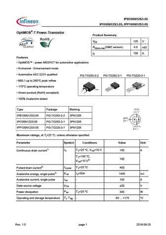
IPB100N12S3-05 IPI100N12S3-05, IPP100N12S3-05 OptiMOS -T Power-Transistor Product Summary VDS 120 V RDS(on),max (SMD version) 4.8 mW ID 100 A Features OptiMOS - power MOSFET for automotive applications N-channel - Enhancement mode Automotive AEC Q101 qualified PG-TO263-3-2 PG-TO262-3-1 PG-TO220-3-1 MSL1 up to 260 C peak reflow 175 C operating temper... See More ⇒
9.14. Size:153K infineon
ipb100n04s2l-03 ipp100n04s2l-03 ipp100n04s2l-03 ipb100n04s2l-03.pdf 

IPB100N04S2L-03 IPP100N04S2L-03 OptiMOS Power-Transistor Product Summary Features V 40 V DS N-channel Logic Level - Enhancement mode R (SMD version) 3.0 m DS(on),max Automotive AEC Q101 qualified I 100 A D MSL1 up to 260 C peak reflow 175 C operating temperature PG-TO263-3-2 PG-TO220-3-1 Green package (lead free) Ultra low Rds(on) 100% Avala... See More ⇒
9.15. Size:195K infineon
ipb100p03p3l-04 ipi100p03p3l-04 ipp100p03p3l-04.pdf 

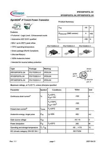
IPB100P03P3L-04 IPI100P03P3L-04, IPP100P03P3L-04 OptiMOS -P Trench Power-Transistor Product Summary V -30 V DS Features R (SMD version) 4 m DS(on),max P-channel - Logic Level - Enhancement mode Automotive AEC Q101 qualified I -100 A D MSL1 up to 260 C peak reflow PG-TO263-3-2 PG-TO262-3-1 PG-TO220-3-1 175 C operating temperature Green package (RoHS Comp... See More ⇒
9.16. Size:155K infineon
ipb100n06s2-05 ipp100n06s2-05.pdf 

IPB100N06S2-05 IPP100N06S2-05 OptiMOS Power-Transistor Product Summary Features V 55 V DS N-channel - Enhancement mode R (SMD version) 4.7 m DS(on),max Automotive AEC Q101 qualified I 100 A D MSL1 up to 260 C peak reflow 175 C operating temperature PG-TO263-3-2 PG-TO220-3-1 Green package (lead free) Ultra low Rds(on) 100% Avalanche tested T... See More ⇒
9.17. Size:258K inchange semiconductor
ipb107n20na.pdf 
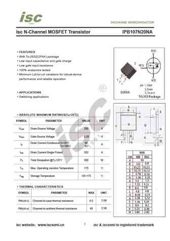
Isc N-Channel MOSFET Transistor IPB107N20NA FEATURES With To-263(D2PAK) package Low input capacitance and gate charge Low gate input resistance 100% avalanche tested Minimum Lot-to-Lot variations for robust device performance and reliable operation APPLICATIONS Switching applications ABSOLUTE MAXIMUM RATINGS(T =25 ) a SYMBOL PARAMETER VALUE UNIT V Drain-Source V... See More ⇒
9.18. Size:258K inchange semiconductor
ipb107n20n3.pdf 
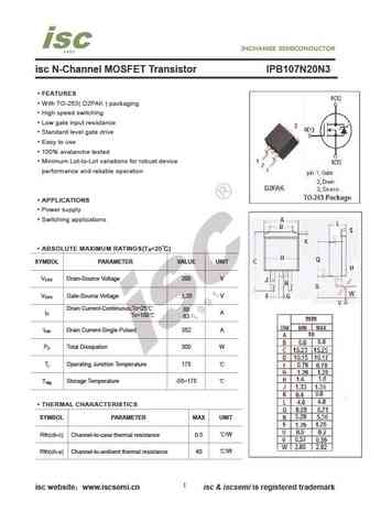
isc N-Channel MOSFET Transistor IPB107N20N3 FEATURES With TO-263( D2PAK ) packaging High speed switching Low gate input resistance Standard level gate drive Easy to use 100% avalanche tested Minimum Lot-to-Lot variations for robust device performance and reliable operation APPLICATIONS Power supply Switching applications ABSOLUTE MAXIMUM RATINGS(T =25 ) a... See More ⇒
Detailed specifications: IPB083N10N3G, IPB08CNE8NG, IPB090N06N3G, IPB093N04LG, IPB096N03LG, IPB097N08N3G, IPB100N04S4-H2, IPB107N20N3G, TK10A60D, IPB114N03LG, IPB120N04S4-01, IPB120N04S4-02, IPB120N06NG, IPB120N06S4-02, IPB120N06S4-H1, IPB123N10N3G, IPB12CNE8NG
Keywords - IPB108N15N3G MOSFET specs
IPB108N15N3G cross reference
IPB108N15N3G equivalent finder
IPB108N15N3G pdf lookup
IPB108N15N3G substitution
IPB108N15N3G replacement
Learn how to find the right MOSFET substitute. A guide to cross-reference, check specs and replace MOSFETs in your circuits.
