IPB114N03LG Specs and Replacement
Type Designator: IPB114N03LG
Type of Transistor: MOSFET
Type of Control Channel: N-Channel
Absolute Maximum Ratings
Pd ⓘ - Maximum Power Dissipation: 38 W
|Vds|ⓘ - Maximum Drain-Source Voltage: 30 V
|Vgs|ⓘ - Maximum Gate-Source Voltage: 20 V
|Id| ⓘ - Maximum Drain Current: 30 A
Tj ⓘ - Maximum Junction Temperature: 175 °C
Electrical Characteristics
tr ⓘ - Rise Time: 3 nS
Cossⓘ - Output Capacitance: 460 pF
Rds ⓘ - Maximum Drain-Source On-State Resistance: 0.0114 Ohm
Package: TO263
IPB114N03LG substitution
- MOSFET ⓘ Cross-Reference Search
IPB114N03LG datasheet
ipb114n03l-g ipp114n03l-g.pdf
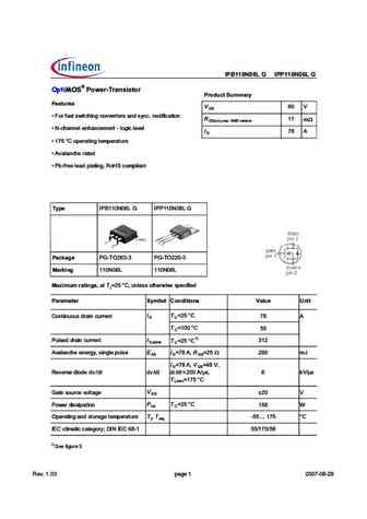
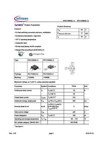
Type IPP114N03L G IPB114N03L G OptiMOS 3 Power-Transistor Product Summary Features V 30 V DS Fast switching MOSFET for SMPS R 11.4 m DS(on),max Optimized technology for DC/DC converters I 30 A D Qualified according to JEDEC1) for target applications N-channel, logic level Excellent gate charge x R product (FOM) DS(on) Very low on-resistance R DS(on... See More ⇒
ipb110p06lm.pdf
IPB110P06LM MOSFET D PAK OptiMOSTM Power Transistor, -60 V Features tab P-Channel Very low on-resistance R @ V =4.5 V DS(on) GS 100% avalanche tested Logic Level Enhancement mode Pb-free lead plating; RoHS compliant 1 Halogen-free according to IEC61249-2-21 3 Product validation Fully qualified according to JEDEC for Industrial Applications Drain t... See More ⇒
ipb117n20nfd.pdf
MOSFET Metal Oxide Semiconductor Field Effect Transistor OptiMOSTM OptiMOSTMFD Power-Transistor, 200 V IPB117N20NFD Data Sheet Rev. 2.0 Final Power Management & Multimarket OptiMOSTMFD Power-Transistor, 200 V IPB117N20NFD D PAK 1 Description Features N-channel, normal level Fast Diode (FD) with reduced Q rr Optimized for hard commutation ruggedness Very low o... See More ⇒
ipb110n20n3lf.pdf
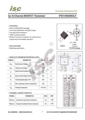
IPB110N20N3LF MOSFET D PAK OptiMOSTM 3 Linear FET, 200 V Features Ideal for hot-swap and e-fuse applications Very low on-resistance R DS(on) Wide safe operating area SOA N-channel, normal level 100% avalanche tested Pb-free plating; RoHS compliant Qualified according to JEDEC1) for target applications Halogen-free according to IEC61249-2-21 Drain ... See More ⇒

Detailed specifications: IPB08CNE8NG , IPB090N06N3G , IPB093N04LG , IPB096N03LG , IPB097N08N3G , IPB100N04S4-H2 , IPB107N20N3G , IPB108N15N3G , AO4407 , IPB120N04S4-01 , IPB120N04S4-02 , IPB120N06NG , IPB120N06S4-02 , IPB120N06S4-H1 , IPB123N10N3G , IPB12CNE8NG , IPB136N08N3G .
History: IPB120N06NG | WML07N100C2
Keywords - IPB114N03LG MOSFET specs
IPB114N03LG cross reference
IPB114N03LG equivalent finder
IPB114N03LG pdf lookup
IPB114N03LG substitution
IPB114N03LG replacement
Need a MOSFET replacement? Our guide shows you how to find a perfect substitute by comparing key parameters and specs
History: IPB120N06NG | WML07N100C2
🌐 : EN ES РУ

LIST
Last Update
MOSFET: HAF1008S | HAF1008L | EMZB08P03H | CS30N20FA9R | AOT66613L | AOSP21313C | AOSP21311C | AOB66918L | AO3415C | AOTF20N40L
Popular searches
bc546 datasheet | mpsa06 transistor | tta004b | 2sc1116 | 2n3565 equivalent | 10n60 | 2sc1061 | a1023