IRFB52N15D Specs and Replacement
Type Designator: IRFB52N15D
Type of Transistor: MOSFET
Type of Control Channel: N-Channel
Absolute Maximum Ratings
Pd ⓘ
- Maximum Power Dissipation: 230 W
|Vds|ⓘ - Maximum Drain-Source Voltage: 150 V
|Vgs|ⓘ - Maximum Gate-Source Voltage: 30 V
|Id| ⓘ - Maximum Drain Current: 51 A
Tj ⓘ - Maximum Junction Temperature: 175 °C
Electrical Characteristics
tr ⓘ - Rise Time: 47 nS
Cossⓘ -
Output Capacitance: 590 pF
RDSonⓘ - Maximum Drain-Source On-State Resistance: 0.032 Ohm
Package: TO220AB
- MOSFET ⓘ Cross-Reference Search
IRFB52N15D datasheet
..1. Size:325K international rectifier
irfb52n15dpbf irfs52n15dpbf.pdf 
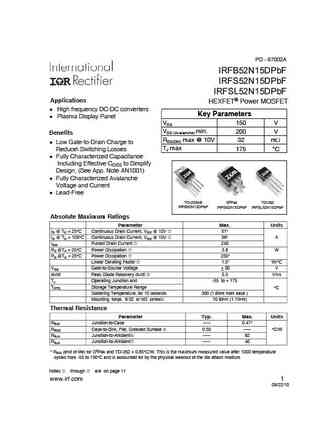
PD - 97002A IRFB52N15DPbF IRFS52N15DPbF IRFSL52N15DPbF Applications HEXFET Power MOSFET l High frequency DC-DC converters Key Parameters l Plasma Display Panel VDS 150 V VDS (Avalanche) min. 200 V Benefits RDS(ON) max @ 10V 32 m l Low Gate-to-Drain Charge to TJ max Reduce Switching Losses 175 C l Fully Characterized Capacitance Including Effective COSS to Simplify Design... See More ⇒
..2. Size:325K international rectifier
irfb52n15dpbf irfs52n15dpbf irfsl52n15dpbf.pdf

PD - 97002A IRFB52N15DPbF IRFS52N15DPbF IRFSL52N15DPbF Applications HEXFET Power MOSFET l High frequency DC-DC converters Key Parameters l Plasma Display Panel VDS 150 V VDS (Avalanche) min. 200 V Benefits RDS(ON) max @ 10V 32 m l Low Gate-to-Drain Charge to TJ max Reduce Switching Losses 175 C l Fully Characterized Capacitance Including Effective COSS to Simplify Design... See More ⇒
..3. Size:245K inchange semiconductor
irfb52n15d.pdf
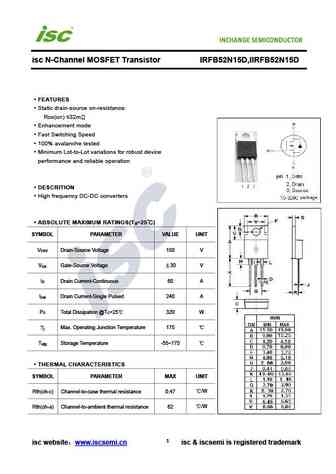
isc N-Channel MOSFET Transistor IRFB52N15D,IIRFB52N15D FEATURES Static drain-source on-resistance RDS(on) 32m Enhancement mode Fast Switching Speed 100% avalanche tested Minimum Lot-to-Lot variations for robust device performance and reliable operation DESCRITION High frequency DC-DC converters ABSOLUTE MAXIMUM RATINGS(T =25 ) a SYMBOL PARAMETER VALUE UNI... See More ⇒
9.1. Size:272K international rectifier
irfb5615pbf.pdf

PD - 96173 DIGITAL AUDIO MOSFET IRFB5615PbF Features Key Parameters Key Parameters Optimized for Class-D Audio VDS 150 V Amplifier Applications RDS(ON) typ. @ 10V m 32 Low RDSON for Improved Efficiency Qg typ. 26 nC Qsw typ. Low QG and QSW for Better THD and Improved 11 nC RG(int) typ. 2.7 Efficiency TJ max 175 C Low QRR for Better THD and Lower EMI ... See More ⇒
9.2. Size:227K international rectifier
irfb59n10dpbf irfs59n10dpbf.pdf
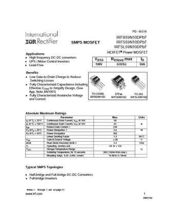
PD - 95378 IRFB59N10DPbF IRFS59N10DPbF SMPS MOSFET IRFSL59N10DPbF HEXFET Power MOSFET Applications l High frequency DC-DC converters VDSS RDS(on) max ID l UPS / Motor Control Inverters 100V 0.025 59A l Lead-Free Benefits l Low Gate-to-Drain Charge to Reduce Switching Losses l Fully Characterized Capacitance Including Effective COSS to Simplify Design, (See App. Note AN1... See More ⇒
9.3. Size:268K international rectifier
irfb5620pbf.pdf
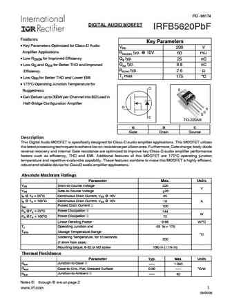
PD - 96174 DIGITAL AUDIO MOSFET IRFB5620PbF Features Key Parameters Key Parameters Optimized for Class-D Audio VDS 200 V Amplifier Applications RDS(ON) typ. @ 10V m 60 Low RDSON for Improved Efficiency Qg typ. 25 nC Low QG and QSW for Better THD and Improved Qsw typ. 9.8 nC RG(int) typ. 2.6 Efficiency TJ max 175 C Low QRR for Better THD and Lower EM... See More ⇒
9.4. Size:227K international rectifier
irfb59n10dpbf irfs59n10dpbf irfsl59n10dpbf.pdf

PD - 95378 IRFB59N10DPbF IRFS59N10DPbF SMPS MOSFET IRFSL59N10DPbF HEXFET Power MOSFET Applications l High frequency DC-DC converters VDSS RDS(on) max ID l UPS / Motor Control Inverters 100V 0.025 59A l Lead-Free Benefits l Low Gate-to-Drain Charge to Reduce Switching Losses l Fully Characterized Capacitance Including Effective COSS to Simplify Design, (See App. Note AN1... See More ⇒
9.5. Size:618K cn evvo
irfb5615.pdf
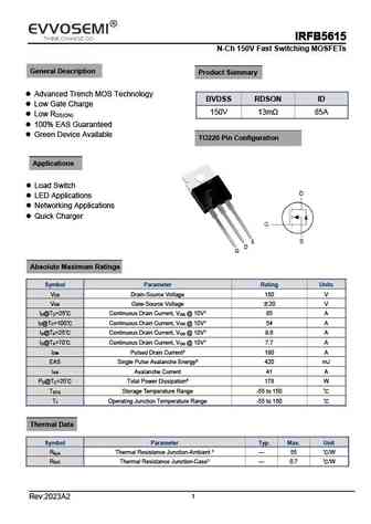
IRFB5615 N-Ch 150V Fast Switching MOSFETs General Description Product Summary Advanced Trench MOS Technology BVDSS RDSON ID Low Gate Charge 150V 13m 85A Low R DS(ON) 100% EAS Guaranteed Green Device Available TO220 Pin Configuration Applications Load Switch LED Applications Networking Applications Quick Charger Absolute Max... See More ⇒
9.6. Size:815K cn vbsemi
irfb59n10d.pdf
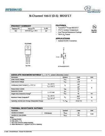
IRFB59N10D www.VBsemi.tw N-Channel 100-V (D-S) MOSFET FEATURES PRODUCT SUMMARY TrenchFET Power MOSFET V(BR)DSS (V) rDS(on) ( )ID (A) 175 C Junction Temperature RoHS 0.018 at VGS = 10 V 100 70a COMPLIANT Low Thermal Resistance Package 100 % Rg Tested APPLICATIONS Isolated DC/DC Converters TO-220AB D G G D S S Top View N-Channel MOSFET ABSOLUTE ... See More ⇒
9.7. Size:246K inchange semiconductor
irfb59n10d.pdf
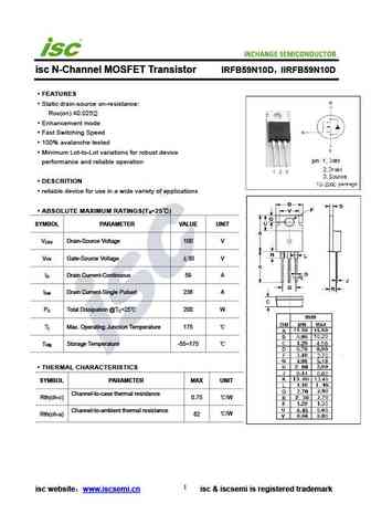
INCHANGE Semiconductor isc N-Channel MOSFET Transistor IRFB59N10D IIRFB59N10D FEATURES Static drain-source on-resistance RDS(on) 0.025 Enhancement mode Fast Switching Speed 100% avalanche tested Minimum Lot-to-Lot variations for robust device performance and reliable operation DESCRITION reliable device for use in a wide variety of applications ABSOLUTE MA... See More ⇒
9.8. Size:244K inchange semiconductor
irfb5620.pdf
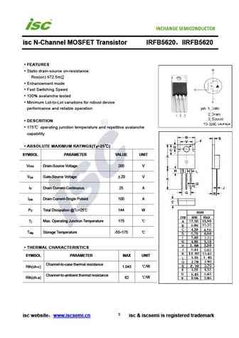
isc N-Channel MOSFET Transistor IRFB5620 IIRFB5620 FEATURES Static drain-source on-resistance RDS(on) 72.5m Enhancement mode Fast Switching Speed 100% avalanche tested Minimum Lot-to-Lot variations for robust device performance and reliable operation DESCRITION 175 operating junction temperature and repetitive avalanche capability ABSOLUTE MAXIMUM RATIN... See More ⇒
9.9. Size:245K inchange semiconductor
irfb5615.pdf
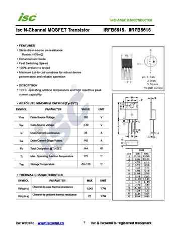
isc N-Channel MOSFET Transistor IRFB5615 IIRFB5615 FEATURES Static drain-source on-resistance RDS(on) 39m Enhancement mode Fast Switching Speed 100% avalanche tested Minimum Lot-to-Lot variations for robust device performance and reliable operation DESCRITION 175 operating junction temperature and high repetitive peak current capability ABSOLUTE MAXIMUM... See More ⇒
Detailed specifications: IRFB4332, IRFB4410, IRFB4410Z, IRFB4410ZG, IRFB4610, IRFB4615, IRFB4620, IRFB4710, 7N65, IRFB5615, IRFB5620, IRFB59N10D, IRFB61N15D, IRFB812, IRFBA1404P, IRFBA1405P, IRFBA90N20D
Keywords - IRFB52N15D MOSFET specs
IRFB52N15D cross reference
IRFB52N15D equivalent finder
IRFB52N15D pdf lookup
IRFB52N15D substitution
IRFB52N15D replacement
Need a MOSFET replacement?
Our guide shows you how to find a perfect substitute by comparing key parameters and specs
