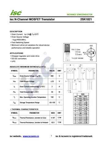
2SK1825 Specs and Replacement
Type Designator: 2SK1825
Type of Transistor: MOSFET
Type of Control Channel: N-Channel
Absolute Maximum Ratings
Pd ⓘ - Maximum Power Dissipation: 0.3 W
|Vds|ⓘ - Maximum Drain-Source Voltage: 50 V
|Vgs|ⓘ - Maximum Gate-Source Voltage: 10 V
|Id| ⓘ - Maximum Drain Current: 0.05 A
Tj ⓘ - Maximum Junction Temperature: 150 °C
Electrical Characteristics
Cossⓘ - Output Capacitance: 5.7 pF
RDSonⓘ - Maximum Drain-Source On-State Resistance: 50 Ohm
Package: MINI
2SK1825 substitution
- MOSFET ⓘ Cross-Reference Search
2SK1825 datasheet
2sk1825.pdf
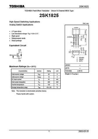
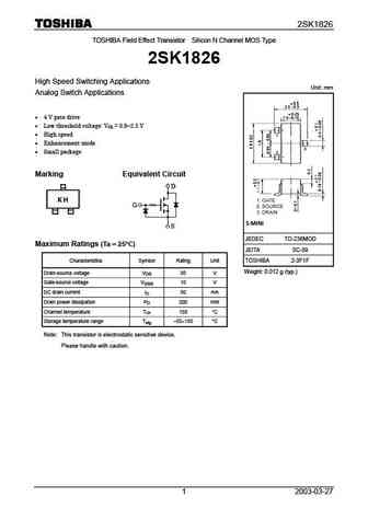
2SK1825 TOSHIBA Field Effect Transistor Silicon N Channel MOS Type 2SK1825 High Speed Switching Applications Unit mm Analog Switch Applications 4 V gate drive Low threshold voltage V = 0.8 2.5 V th High speed Enhancement-mode Small package Equivalent Circuit JEDEC Maximum Ratings (Ta = = 25 C) = = JEITA Characteristics Symbol Rat... See More ⇒
2sk1824.pdf
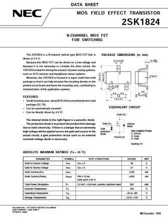
DATA SHEET MOS FIELD EFFECT TRANSISTOR 2SK1824 N-CHANNEL MOS FET FOR SWITCHING The 2SK1824 is a N-channel vertical type MOS FET that is PACKAGE DIMENSIONS (in mm) driven at 2.5 V. 0.3 0.05 0.1+0.1 0.05 Because this MOS FET can be driven on a low voltage and because it is not necessary to consider the drive current, the 2SK1824 is ideal for driving the actuator of power-saving ... See More ⇒
2sk1827.pdf
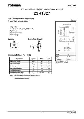
2SK1827 TOSHIBA Field Effect Transistor Silicon N Channel MOS Type 2SK1827 High Speed Switching Applications Unit mm Analog Switch Applications 4 V gate drive Low threshold voltage V = 0.8 2.5 V th High speed Enhancement-mode Small package Marking Equivalent Circuit JEDEC Maximum Ratings (Ta = = 25 C) = = JEITA SC-70 Characteristics Sy... See More ⇒
2sk1828.pdf
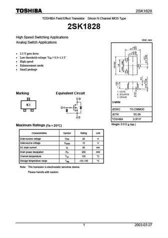
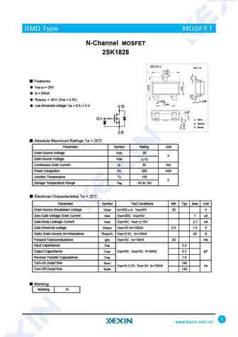
2SK1828 TOSHIBA Field Effect Transistor Silicon N Channel MOS Type 2SK1828 High Speed Switching Applications Unit mm Analog Switch Applications 2.5 V gate drive Low threshold voltage V = 0.5 1.5 V th High speed Enhancement-mode Small package Marking Equivalent Circuit JEDEC TO-236MOD JEITA SC-59 TOSHIBA 2-3F1F Weight 0.012 g (typ.) Maximum Ra... See More ⇒

Detailed specifications: TPCT4201, TPCT4202, TPCT4203, TPCT4204, 2SJ148, 2SJ167, 2SJ342, 2SK1061, NCEP15T14, 2SK982, SSM3J15TE, SSM3J16TE, SSM3K03FE, SSM3K03FV, SSM3K03TE, SSM3K04FE, SSM3K04FS
Keywords - 2SK1825 MOSFET specs
2SK1825 cross reference
2SK1825 equivalent finder
2SK1825 pdf lookup
2SK1825 substitution
2SK1825 replacement
Learn how to find the right MOSFET substitute. A guide to cross-reference, check specs and replace MOSFETs in your circuits.
History: 2SK3376CT | WMN80R720S
🌐 : EN ES РУ

LIST
Last Update
MOSFET: ASU70R600E | ASU65R850E | ASU65R550E | ASU65R350E | ASR65R120EFD | ASR65R046EFD | ASQ65R046EFD | ASM65R280E | ASM60R330E | ASE70R950E
Popular searches
2sd330 | 20n60 | ksa1013 | mje15032g datasheet | 2sc2166 | 2sc5198 | 2sc1971 | tip41c transistor datasheet