BUK9840-55 Specs and Replacement
Type Designator: BUK9840-55
Type of Transistor: MOSFET
Type of Control Channel: N-Channel
Absolute Maximum Ratings
Pd ⓘ
- Maximum Power Dissipation: 1.8 W
|Vds|ⓘ - Maximum Drain-Source Voltage: 55 V
|Vgs|ⓘ - Maximum Gate-Source Voltage: 10 V
|Id| ⓘ - Maximum Drain Current: 5 A
Tj ⓘ - Maximum Junction Temperature: 150 °C
Electrical Characteristics
RDSonⓘ - Maximum Drain-Source On-State Resistance: 0.04 Ohm
Package: SOT223
- MOSFET ⓘ Cross-Reference Search
BUK9840-55 datasheet
..1. Size:59K philips
buk9840-55 2.pdf 

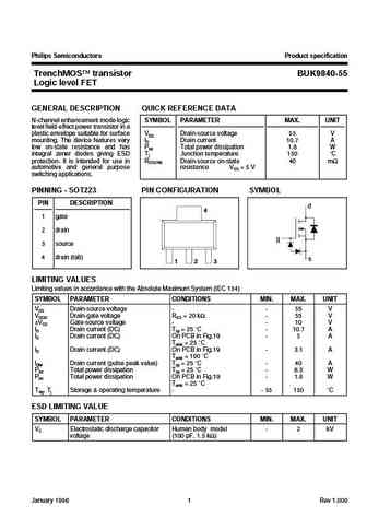
Philips Semiconductors Product specification TrenchMOS transistor BUK9840-55 Logic level FET GENERAL DESCRIPTION QUICK REFERENCE DATA N-channel enhancement mode logic SYMBOL PARAMETER MAX. UNIT level field-effect power transistor in a plastic envelope suitable for surface VDS Drain-source voltage 55 V mounting. The device features very ID Drain current 10.7 A low on-state resistanc... See More ⇒
..2. Size:59K infineon
buk9840-55 2.pdf 

Philips Semiconductors Product specification TrenchMOS transistor BUK9840-55 Logic level FET GENERAL DESCRIPTION QUICK REFERENCE DATA N-channel enhancement mode logic SYMBOL PARAMETER MAX. UNIT level field-effect power transistor in a plastic envelope suitable for surface VDS Drain-source voltage 55 V mounting. The device features very ID Drain current 10.7 A low on-state resistanc... See More ⇒
..3. Size:885K cn vbsemi
buk9840-55.pdf 

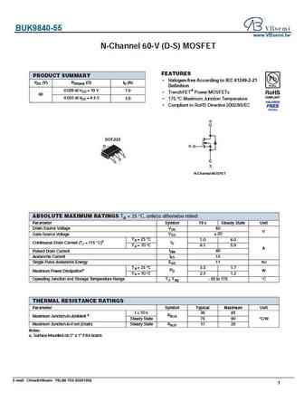
BUK9840-55 www.VBsemi.tw N-Channel 60-V (D-S) MOSFET FEATURES PRODUCT SUMMARY Halogen-free According to IEC 61249-2-21 VDS (V) RDS(on) ( )ID (A) Definition 0.029 at VGS = 10 V 7.0 TrenchFET Power MOSFETs 60 0.033 at VGS = 4.5 V 5.6 175 C Maximum Junction Temperature Compliant to RoHS Directive 2002/95/EC D SOT-223 D G S D G S N-Channel MOSFET... See More ⇒
9.1. Size:295K philips
buk98150 55a-01.pdf 

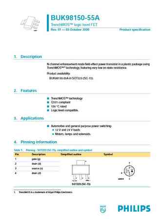
BUK98150-55A TrenchMOS logic level FET Rev. 01 03 October 2000 Product specification M3D087 1. Description N-channel enhancement mode field-effect power transistor in a plastic package using TrenchMOS 1 technology, featuring very low on-state resistance. Product availability BUK98150-55A in SOT223 (SC-73). 2. Features TrenchMOS technology Q101 compliant 150 C rated... See More ⇒
9.2. Size:54K philips
buk98150-55 2.pdf 

Philips Semiconductors Product specification TrenchMOS transistor BUK98150-55 Logic level FET GENERAL DESCRIPTION QUICK REFERENCE DATA N-channel enhancement mode logic SYMBOL PARAMETER MAX. UNIT level field-effect power transistor in a plastic envelope suitable for surface VDS Drain-source voltage 55 V mounting. The device features very ID Drain current 5.5 A low on-state resistanc... See More ⇒
9.3. Size:56K philips
buk9830-30 1.pdf 

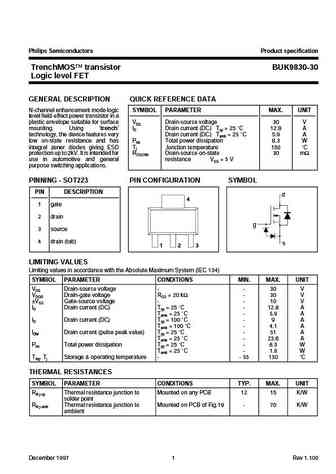
Philips Semiconductors Product specification TrenchMOS transistor BUK9830-30 Logic level FET GENERAL DESCRIPTION QUICK REFERENCE DATA N-channel enhancement mode logic SYMBOL PARAMETER MAX. UNIT level field-effect power transistor in a plastic envelope suitable for surface VDS Drain-source voltage 30 V mounting. Using trench ID Drain current (DC) Tsp = 25 C 12.8 A technology... See More ⇒
9.4. Size:55K philips
buk9880-55 2.pdf 

Philips Semiconductors Product specification TrenchMOS transistor BUK9880-55 Logic level FET GENERAL DESCRIPTION QUICK REFERENCE DATA N-channel enhancement mode logic SYMBOL PARAMETER MAX. UNIT level field-effect power transistor in a plastic envelope suitable for surface VDS Drain-source voltage 55 V mounting. The device features very ID Drain current 7.5 A low on-state resistance... See More ⇒
9.5. Size:711K nxp
buk98180-100a.pdf 

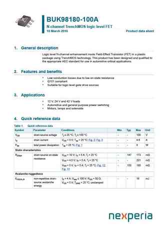
BUK98180-100A N-channel TrenchMOS logic level FET 16 March 2016 Product data sheet 1. General description Logic level N-channel enhancement mode Field-Effect Transistor (FET) in a plastic package using TrenchMOS technology. This product has been designed and qualified to the appropriate AEC standard for use in automotive critical applications. 2. Features and benefits Low conduction... See More ⇒
9.6. Size:967K nxp
buk9832-55a.pdf 

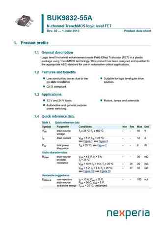
BUK9832-55A N-channel TrenchMOS logic level FET Rev. 02 1 June 2010 Product data sheet 1. Product profile 1.1 General description Logic level N-channel enhancement mode Field-Effect Transistor (FET) in a plastic package using TrenchMOS technology. This product has been designed and qualified to the appropriate AEC standard for use in automotive critical applications. 1.2 Features ... See More ⇒
9.7. Size:716K nxp
buk9875-100a.pdf 

BUK9875-100A N-channel TrenchMOS logic level FET 19 March 2014 Product data sheet 1. General description Logic level N-channel enhancement mode Field-Effect Transistor (FET) in a plastic package using TrenchMOS technology. This product has been designed and qualified to the appropriate AEC standard for use in automotive critical applications. 2. Features and benefits Low conduction ... See More ⇒
9.8. Size:744K nxp
buk98150-55a.pdf 

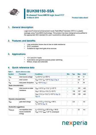
BUK98150-55A N-channel TrenchMOS logic level FET 19 March 2014 Product data sheet 1. General description Logic level N-channel enhancement mode Field-Effect Transistor (FET) in a plastic package using TrenchMOS technology. This product has been designed and qualified to the appropriate AEC standard for use in automotive critical applications. 2. Features and benefits Low conduction ... See More ⇒
9.9. Size:735K nxp
buk9880-55a.pdf 

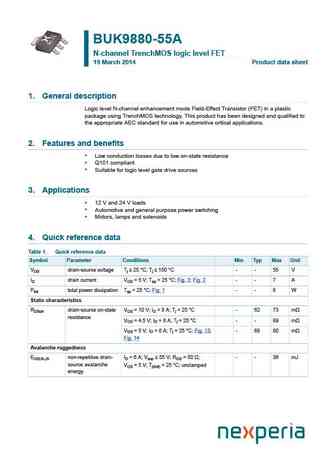
BUK9880-55A N-channel TrenchMOS logic level FET 19 March 2014 Product data sheet 1. General description Logic level N-channel enhancement mode Field-Effect Transistor (FET) in a plastic package using TrenchMOS technology. This product has been designed and qualified to the appropriate AEC standard for use in automotive critical applications. 2. Features and benefits Low conduction l... See More ⇒
9.10. Size:55K infineon
buk9880-55 2.pdf 

Philips Semiconductors Product specification TrenchMOS transistor BUK9880-55 Logic level FET GENERAL DESCRIPTION QUICK REFERENCE DATA N-channel enhancement mode logic SYMBOL PARAMETER MAX. UNIT level field-effect power transistor in a plastic envelope suitable for surface VDS Drain-source voltage 55 V mounting. The device features very ID Drain current 7.5 A low on-state resistance... See More ⇒
9.11. Size:897K cn vbsemi
buk9832-55.pdf 

BUK9832-55 www.VBsemi.tw N-Channel 60-V (D-S) MOSFET FEATURES PRODUCT SUMMARY Halogen-free According to IEC 61249-2-21 VDS (V) RDS(on) ( )ID (A) Definition 0.029 at VGS = 10 V 7.0 TrenchFET Power MOSFETs 60 0.033 at VGS = 4.5 V 5.6 175 C Maximum Junction Temperature Compliant to RoHS Directive 2002/95/EC D SOT-223 D G S D G S N-Channel MOSFET... See More ⇒
9.12. Size:1496K cn vbsemi
buk98150-55.pdf 

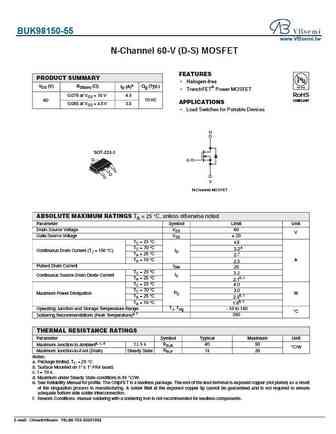
BUK98150-55 www.VBsemi.tw N-Channel 60-V (D-S) MOSFET FEATURES PRODUCT SUMMARY Halogen-free VDS (V) RDS(on) ( ) ID (A)a Qg (Typ.) TrenchFET Power MOSFET 0.076 at VGS = 10 V 4.5 RoHS 10 nC COMPLIANT 60 APPLICATIONS 0.085 at VGS = 4.5 V 3.5 Load Switches for Portable Devices D SOT-223-3 D G S D G S N-Channel MOSFET ABSOLUTE MAXIMUM RATINGS TA = 25 C, unl... See More ⇒
Detailed specifications: BUK9620-55
, BUK9624-55
, BUK9628-55
, BUK9635-55
, BUK9675-55
, BUK9775-55
, BUK98150-55
, BUK9830-30
, AOD4184A
, BUK9880-55
, BUP60
, BUP61
, BUP62
, BUP63
, BUP64
, BUP65
, BUP66
.
History: HAT2039R
Keywords - BUK9840-55 MOSFET specs
BUK9840-55 cross reference
BUK9840-55 equivalent finder
BUK9840-55 pdf lookup
BUK9840-55 substitution
BUK9840-55 replacement
Can't find your MOSFET?
Learn how to find a substitute transistor by analyzing voltage, current and package compatibility

